Sandia National Labs SA3000 8085 CPU
![]() Back in the late 1970’s and early 1980’s Sandia National Laboratory (in Albuquerque NM USA) began building the capacity to design, fab, and test IC’s at scale (packaging was handled by Fairchild and Allied Signal). Why would a National Laboratory need the capacity to do this? To provide components that were not available commercially. In this case, Sandia’s goal was to make radiation hardened devices for use in weapons and space missions. The harshest environments and where reliability was paramount.
Back in the late 1970’s and early 1980’s Sandia National Laboratory (in Albuquerque NM USA) began building the capacity to design, fab, and test IC’s at scale (packaging was handled by Fairchild and Allied Signal). Why would a National Laboratory need the capacity to do this? To provide components that were not available commercially. In this case, Sandia’s goal was to make radiation hardened devices for use in weapons and space missions. The harshest environments and where reliability was paramount.
Sandia began their fab in 1978 on 2″ wafers on a 10u process, a few generations behind ‘state of the art’. By 1982 this was upgraded to a 4″ wafer system with features as small as 2u. This was the design node that Sandia used to make all the IC’s used in the Galileo space probe (for its mission to Jupiter). This included the 1802 processor from RCA. Sandia received the logic diagrams of the processor and its support chips and recreated them in a radiation hardened process. How many IC’s were needed? Over 50,000 for the probe itself, backups, testing chips etc.
 Sandia also produced various IC’s for weapons’ systems, and not things like tanks or planes or ships, but weapons that need IC’s that can handle intense radiation, these were generally nuclear warheads, reentry vehicles, ICBMs and things along those lines. Sandia made the chips for them, as well as maintains a ‘war reserve’ stock of replacement ICs for when they are needed.
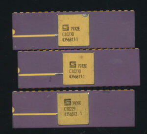
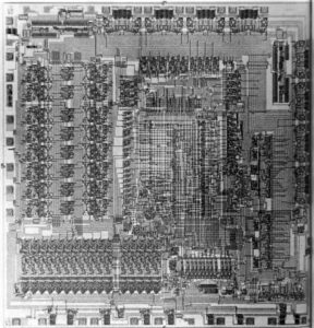
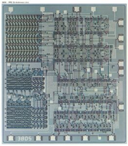
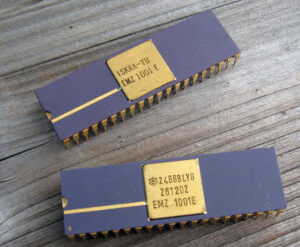
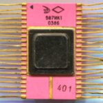
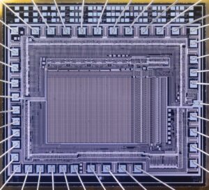
In 1982 Sandia began work on a CMOS rad-hard conversion of the Intel 8085 processor. This would become the Sandia SA3000. Converting the HMOS Intel 8085 to a rad hard CMOS process took some doing. The original 8085 had around 6500 transistors. Converting it to CMOS resulted in a 18,000 transistor device. One of the trickier conversions was the instruction decoder (a large PLA), easy in NMOS, less so in CMOS. The SA3000 was made on 4″ wafers on a 3u process.
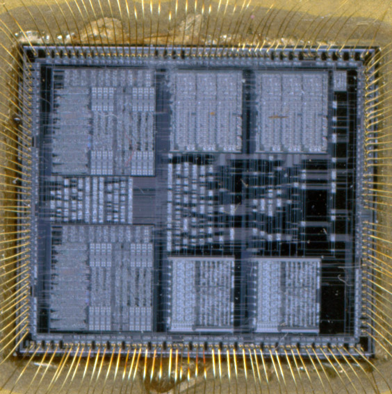
Sandia SA3000 – Lot G Wafer 18 – Made in 1984
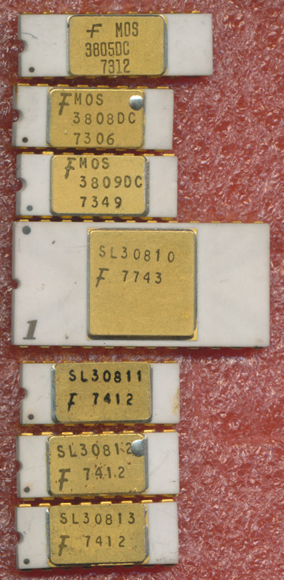
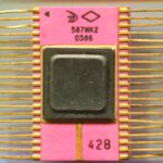
Die size was 228-239 mils and it operated at 4.5-11V, while maintaining compatibility at 5V for testing. The increased voltage gives a lot more ‘head room’ for radiation effects, as radiation exposure tends to slow the max device speed down. Sandia also made a set of support chips for the SA3000, the SA3001 (Intel 8155), the SA3002 (Intel 8355), SA3026 (Intel 8212) and many others as needed.
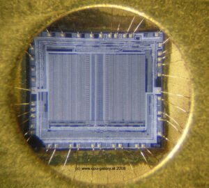
SA3001 – Intel 8155
Designing for radiation hardness is an art and a science, much went into the design to make it work reliably. The chips were made on a n-on-n+ epitaxial substrate to provide latchup control, extensive guard rings around transistors were used and hardened oxides (largely a process of controlling production temps). Contact of power to the substrate and ground to the guardband and p-well is made as often as possible to further aid in latchup control.
 |
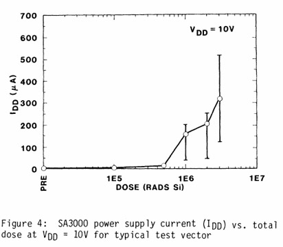 |
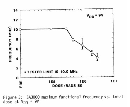
What did this get Sandia? An 8085 processor that could handle 1×10⁶ rads of radiation with only a 25% reduction in performance, and 3×10⁶ rads with a 40% drop. The design goal was 1×10⁵ so they greatly exceeded that. Anything over 1000 rads in generally fatal for humans.
 |
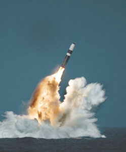 |
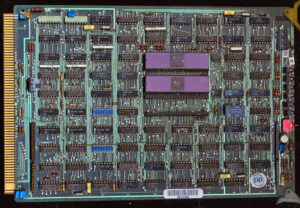
| W88 Warhead control portion | Trident II (up to 8 SA3000 CPUs) |
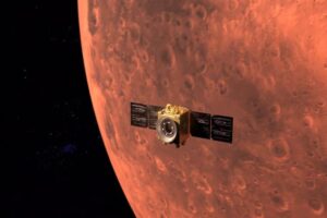
The SA3000 was used (and still is) in the W88 475kt nuclear warhead used on the Submarine launched Trident II. It runs the main computer/programmer responsible for altitude and fuzing calculations. The SA3000 was also used by Ball aerospace for a deep space star tracker design and used on the Combined Release and Radiation Effects Satellite (CRRES) in 1990 to study the effects of high radiation on electronics. The electronics on the CRRES worked fine, but the battery failed after only a year causing an early mission failure.
 |
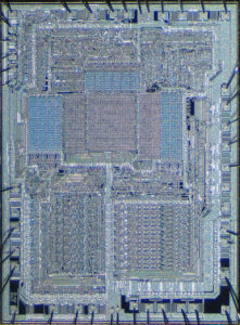 |
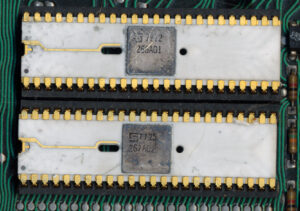
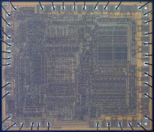
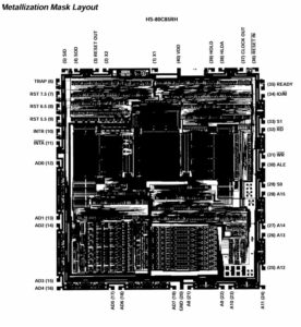
| Harris/Sandia die CMOS 80c85 | Intel 8085A die |
In around 1984-1985 the govt decided to bring in a contractor to run the fab much to the annoyance of Sandia management and detriment to efficiency. This would be Allied Signal, who at that point had no experience running fab’s. This greatly slowed down production for some time.
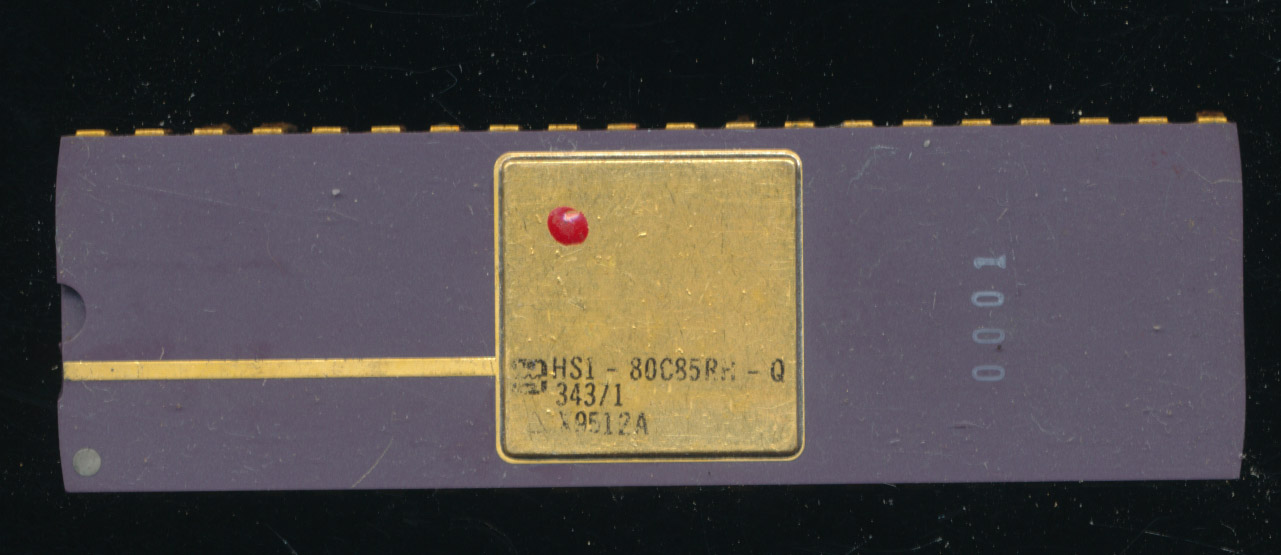
Harris HS1-80C85RH-Q
Serial # 0001
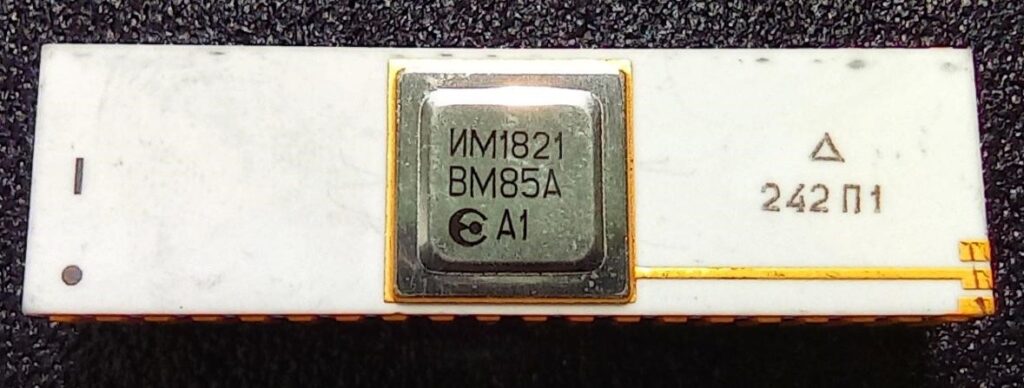
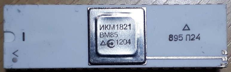
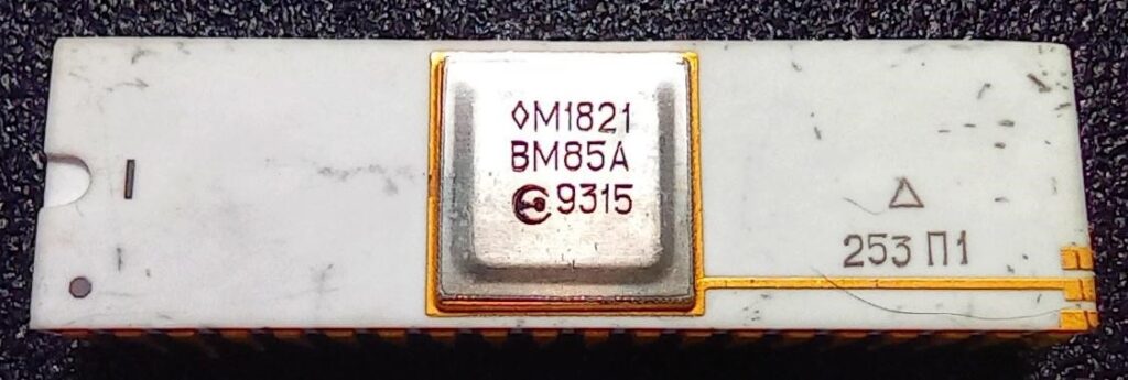
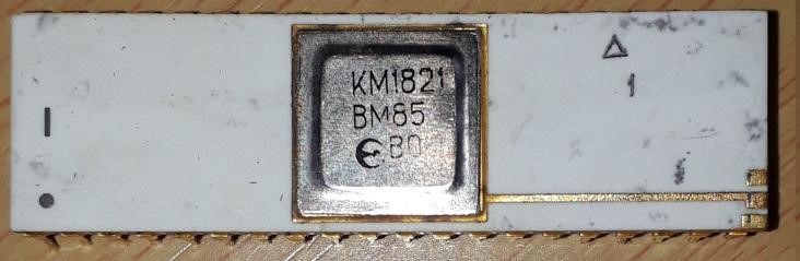
The SA3000 (and its support chips) were commercialized by Harris in 1990 as the HS1-80C85RH and the HS9-80C85RH. These are similar to the SA3000, made on the same process, but spec’d with only a 5V operating voltage rather than 10V and a max speed of 2MHz rather then the 10MHz the SA3000 is capable of. The HS1 is space grade, with higher levels of screening, and the HS9 is military grade, but not screened to space use levels.
Posted in:
CPU of the Day