October 1st, 2019 ~ by admin

The Story of the IBM Pentium 4 64-bit CPU

Introduction

This time we will talk about one unique Intel processor, which did not appear on the retail market and whose reviews you will not find on the Internet. This processor was produced purely by special order for one well-known manufacturer of computer equipment. Also in the framework of this article I will try to assemble one of the most powerful retro-systems with this processor.

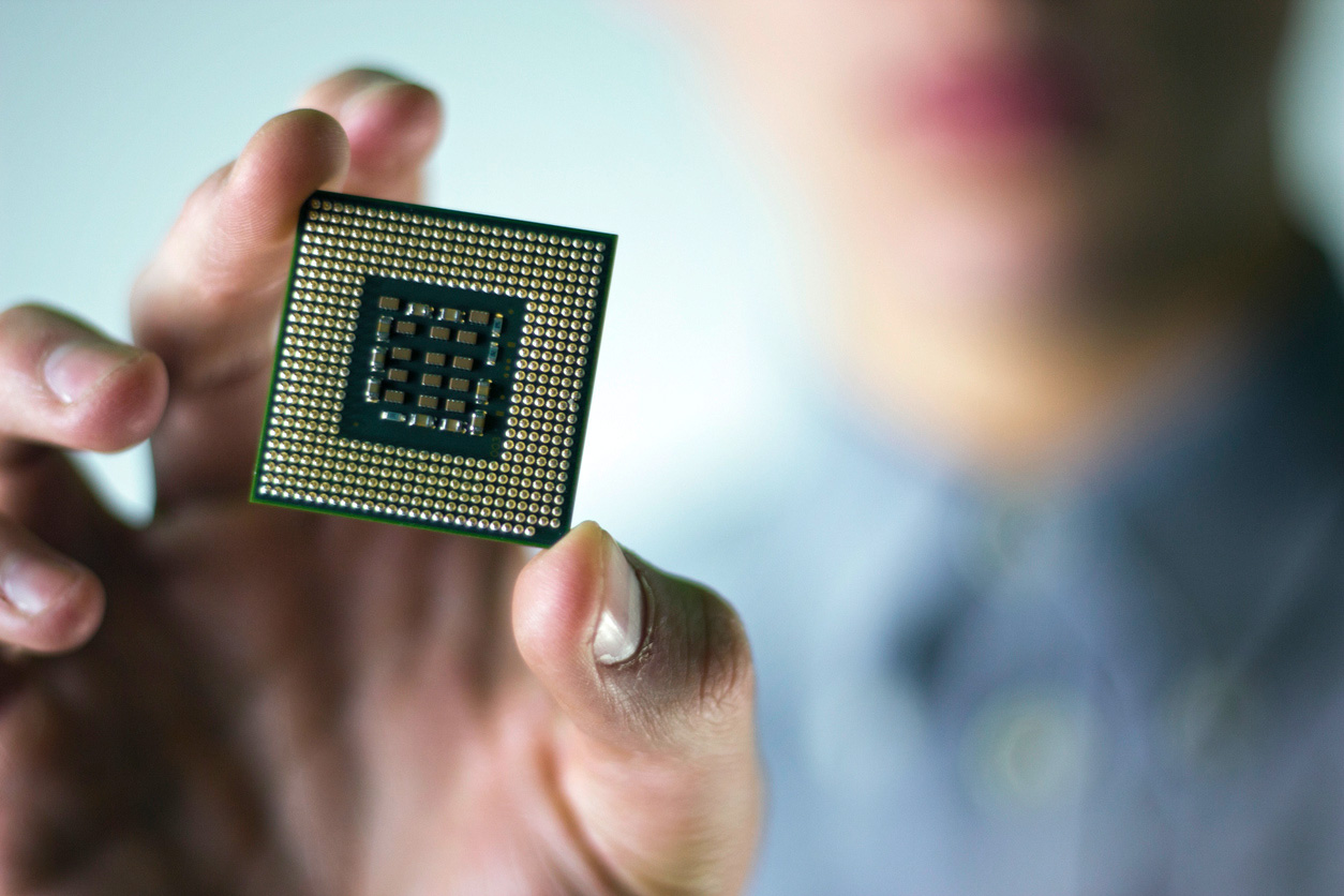
From the title of the article, I think many people understand that we will talk about the Socket 478 Intel processor

Most people are familiar with the Socket 478 that replaced Socket 370 at the end of 2001 (we omit Socket 423 due to its short lifespan of less then a year) and allowed the use of single-core, and then with Hyper Threading technology “pseudo-dual” processors that can perform two tasks in parallel. All production Intel processors within Socket 478 were 32-bit, even a couple of representatives from the Pentium Extreme Edition server segment on the «Gallatin» core. But as always there are exceptions. And this exception, or to be more precise, two exceptions, were two models of Pentium 4 processors with the Prescott core, which had 64-bit instructions (EM64T) at their disposal.

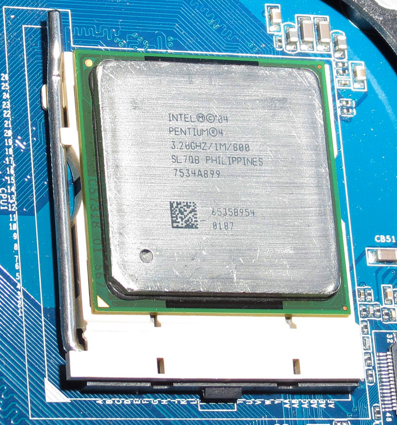
Intel Pentium 4 SL7QB 3.2GHz: 64-bits on S478

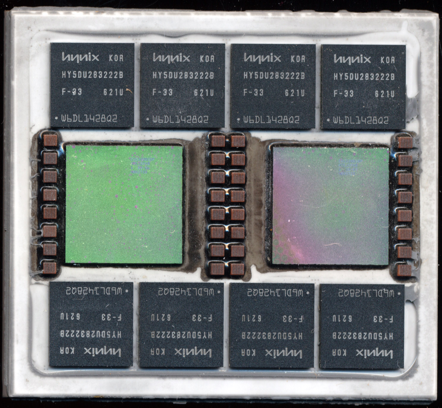
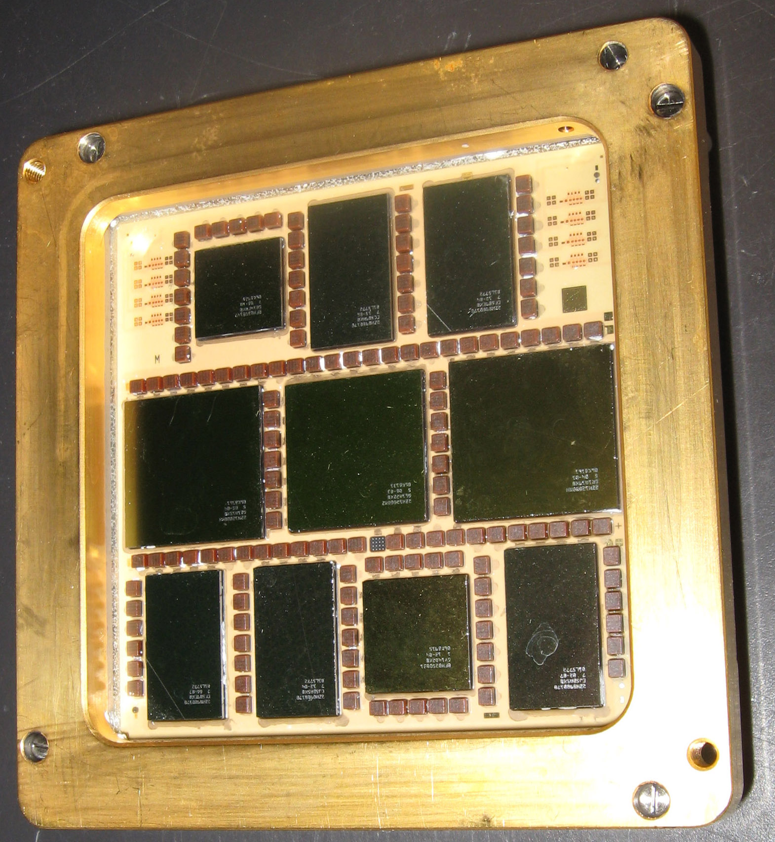
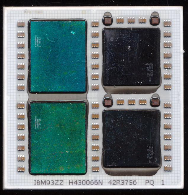
This pair of processors were commissioned by IBM for its eServer xSeries servers. These processors never hit the retail market and their circulation was not very large, so finding them now is very problematic. It is interesting that the fact that if you want and naturally have the right amount of money, or a large enough order, you can count on a special order of the processor that is needed for the specific needs, with characteristics that will be unique and will not be repeated in standard production products. And it should be noted that not a few such processors have been released, in fact, in the 70’s and early 80’s this was the very purpose of the now ubiquitous ‘sspec.’ Chips with an Sspec (Specification #) were chips that had some specification DIFFERENT from the standard part/datasheet.  A chip WITHOUT a sspec was a standard product.  By the late 1980’s all chips began to receive sspecs as a means of tracking things like revisions, steppings, etc.  I will talk about some a little later.

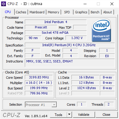
hat’s how the processor looks through the eyes of the CPU-Z utility. In the “Instructions” field after SSE3, the EM64T proudly shows off! Link to popular CPU-Z Validation.

Special processors made for IBM belonged to the Prescott core and were based on E0 stepping with support for 64-bit instructions, which is not typical for Socket 478! The first 64-bit CPUs for “everyone” appeared only with the arrival of the next LGA775 socket, and even then it wasn’t right away; some Pentium 4 models in LGA775 version were 32-bit. I specifically pointed out that the Pentium 4 Socket 478 model with EM64T support belonged to the E0-stepping, although later the more advanced stepping G1 was released, which did not have such innovations. The first model worked at a frequency of 3.2 GHz and had a SPEC code – SL7QB, the second was slightly faster with a frequency of 3.4 GHz and the SPEC code – SL7Q8.

For the rest, these were the usual «Prescott». But the presence of 64-bit instructions made these processors unique, capable of working with 64-bit operating systems and the same applications, allowing them to do what their 32-bit comrades simply could not do.

Read More »

October 20th, 2016 ~ by admin

Processors to Emulate Processors: The Palladium II

Cadence Palladium II Processor MCM 1536 cores - 128MB GDDR - Manufactured by IBM

Cadence Palladium II Processor MCM 1536 cores – 128MB GDDR – Manufactured by IBM

Several years ago we posted an unusual MCM that’s purpose was a mystery.  It was clearly made by IBM and clearly high end.  While researching another mystery IBM MCM both of their identities came to light.  The original MCM is an emulation processor from a Cadence Palladium Emulator/Accelerator system.

In the 1990’s IBM had been working on technology to make emulating hardware/software designs more efficient as such designs got more complicated.  At the time it was most common to emulate a system in an FPGA for testing, but as designs grew more complex this became a slower and slower process.  IBM developed the idea of an emulation processor.  This was to be known as CoBALT (Concurrent Broadcast Array Logic Technology).  It was licensed to a company called QuickTurn in 1996.  At its heart the QuickTurn CoBALT was a massively parallel array of boolean logic processors.  Boolean processors are similar to a normal processor

Here is a flipped (and very rough) die from a Palladium II. You can make out the very repeating design of the 768 boolean processors.

Here is a flipped (and very rough) die from a Palladium II. You can make out the very repeating design of the 768 boolean processors.

but only handle boolean data, logic functions such as AND, OR, XOR, etc.  Perhaps the most well known, is the boolean sub-processor that Intel built into the 8051, it excelled at bit manipulation.  The same applies for the emulation processors in CoBALT.  Each boolean processor has at its heart a LUT (Look Up Table), with 8-bits to encode the logic function (resulting in 256 possible logic function outputs) and the 3 gate inputs serving as an index into the LUT, as well as the associated control logic, networking logic, etc.

A target design is compiled and emulated by the CoBALT system.  The compiling is the tricky part, the entire design is broken down into 3-input logic gates, allowing the emulator to emulate any design.  Each processor element can handle one logic function, or act as a memory cell (as many designs obviously include memory).  The CoBALT had 65 processors per chip, and 65 chips per board, with a system supporting up to 8 boards.  This 33,280 processor system could compile 2 Million gates/Hour.  The CoBALT plus sped this up a bit and supported 16 boards, doubling capacity and added on board memory.

Read More »

March 11th, 2014 ~ by admin

IBM z800 MCM Mainframe Processor

IBM z800 MCM

IBM z800 MCM

Mainframes are the workhorses of the computing industry.  They process transactions for about every industry, and handle the brunt of the economy.  Their MTBF (Mean Time Between Failures) is measured in decades (typically 20-50 years).  A comparison to a home computer is hard to make, they are in an entirely different league, playing an entirely different game.

Data Intense vs. CPU Intense

Mainframe processors such as these work in what is referred to as ‘Data Intensive’ computing environments.  This is different from multi-cored processing that focuses on ‘CPU Intensive’ computing.  CPU intense has a relatively small data set, but most perform a lot of work on that set of data, or do the same instruction on a set of data (such as graphics).  CPU Intense processing can often be sped up with the addition of more processing cores.  Data Intense processing does not see as much benefit from adding cores.  Its biggest bottleneck is accessing the data, thus the System z tends to have VERY large caches, and very high bandwidth memory.  They typically operate on transactional type data, where the processing has to operate in a certain order (A has to be done before B which has to finish before C etc).

IBM was one of the first, and continues to be one of the largest suppliers of such systems.  Starting with the System/360 introduced in 1964 to the zSeries today.  The zSeries was first launched in 2000 with the z900, a significant upgrade from the System/390.  Data addressing was moved to 64-bits (from 31 bits) yet backwards compatibility (all the way back to the 360) is maintained.  The z900 ran at 775MHz and was built with a 35 die MCM containing 20 Processing Units (PUs) and 32MB of L2 Cache.

Read More »

Tags:
,

Posted in:
CPU of the Day

February 18th, 2014 ~ by admin

CPU of the Day: IBM POWER5+ QCM

IBM POWER5+ QCM - 4 dies, 8 cores, and 72MB of L3 Cache

IBM POWER5+ QCM – 4 dies, 8 cores, and 72MB of L3 Cache

When the POWER5 processor was released in 2004 it was made in two versions, a DCM (Dual Chip Module) containing a POWER5 die and its 36MB L3 cache die, as well as a MCM containing 4 POWER5 die and 4 L3 cache dies totaling 144MB.  The POWER5 is a dual core processor, thus the DCM was a dual core, and the MCM an 8 core processor.  The POWER5 contains 276 million transistors and was made on a 130nm CMOS9S process.

In 2005 IBM shrank the POWER5 onto a 90nm CMOS10S manufacturing process resulting in the POWER5+.  This allowed speeds to increase to 2.3GHz from the previous max of 1.9GHz.  The main benefit from the process shrink was less power draw, and thus less heat.  This allowed IBM to make the POWER5+ in a QCM (Quad Chip Module) as well as the previous form factors.  The QCM ran at up to 1.8GHz and contained a pair of POWER5+ dies and 72MB of L3 Cache.

The POWER5+ was more then a die shrink, IBM reworked much of the POWER5 to improve performance, adding new floating point instructions, doubling the TLB size, improved SMP support, and an enhanced memory controller to mention just a few.

The result? A much improved processor and a very fine looking QCM.

Tags:
, ,

Posted in:
CPU of the Day

August 8th, 2013 ~ by admin

How To: Disassembling an IBM POWER4 MCM

The  IBM POWER4 was released in 2001.  It was a 1.1-1.9GHz dual core processor widely used in IBM’s server line including the RS/6000 and AS/400.  It can be commonly found as a single chip dual core, but also as a large MCM containing 4 POWER4 dies. These MCMs include a very large and heavy aluminium heatsink attached to a solid copper housing.  The complete unit weighs in at a hefty 3kg.  The heatsink and housing can be removed revealing a 230 gram MCM (with its small heat spreaders).

IBM POWR4 MCM disassembly

To disassemble one of these you will need a variety of tools.  A 4 mm socket, hex bits (2.5, 3 and 4mm), T8 torx bit , a medium flat tip screw driver, gloves and a good heat source (I use a propane torch)

Remove the Interposer and screws

First remove the 4 T8 torx screws that hold the interposer to the module.  It gets in the way and can melt easily.  Also remove the 8 3mm screws around the perimeter.  These hold the aluminium heatsink to the copper housing.

Read More »

Tags:
, ,

Posted in:
How To

July 26th, 2013 ~ by admin

Apple G3 Prototype: The Goleta and IBM Arthur Processor

IBM Arthur Processor - 1997

IBM Arthur Processor – 1997

By 1997 the PowerPC 604e was getting a bit dated.  Apple needed an updated faster processor for their new computers and IBM and Motorola needed a new processor to sell to Apple.  The PowerPC 750 was an evolution of the 604e and became the core of Apple’s various G3 systems.

In early 1997 Apple , IBM, and Motorola (together known as the AIM Alliance) were working on what would become the PowerPC 750.  It’s code name? The Arthur.  Apparently someone at IBM or Motorola had a liking for Sherlock Holmes as the 745 was codenamed Conan and the 755 Doyle, after Sir Arthur Conan Doyle, writer of Sherlock Holmes.  This particular part is date coded R20003PAP which means it was made in mid-May of 1997, 6 months before the G3 and PowerPC 750 were officially released.

The card the Arthur processor (hand labeled 300Mhz) resides on is an Apple Prototype known as the Goleta.  The Goleta was one of the first Apple G3 products.   It was to be used in the PowerMac 9700 aka the PowerExpress which was to be a 6 slot G3 PowerMac running at 275MHz.

Apple Goleta G3 Prototype

Apple Goleta G3 Prototype – Click here to see the full card.

It never made it past the prototype stage.  The card is labeled as serial #014 making it a very early prototype, though how many total were made is not known.  The card may have been used at Apple for testing other deigns as well and certainly was a test bench for the new 750 PowerPC Processor.  This was a chaotic time for Apple as they were struggling to pull out of near bankruptcy.  Steve Jobs had only just returned to the company and radically changed what Apple was doing, and what they were not doing (making money).

Posted in:
CPU of the Day

March 22nd, 2013 ~ by admin

CPU of the Day: IBM Micro/370 – True Mainframe on a chip

IBM System/370 - 1970

IBM System/370 – 1970

IBM introduced the 12.5MHz cabinet sized System/370 in June 1970 as an evolution of the System/360 from 1964.  These systems formed the entire base of IBM’s mainframe business.  Today’s System z, itself an evolution of the original System/360 and 370, can still run many of the original programs, unmodified, from 50 years ago.  This is a testament to 2 things, the wide adoption of the IBM systems, and the forward thinking of IBM.  Even the original System/360 from 1964 was a full 32-bit computer.  Single chip processors did not embrace 32 bit architectures until the very early 1980’s (Motorola 68k, National 32k, etc).

In 1980 IBM sought to make a single chip version of the 370, in an effort to make a version that could be used for desktop type computers.  This was to become the Micro/370.  There were 2 distinct products to come out of this goal that are widely confused and debated.  The first became the PC XT/370, an add in card(s) for an IBM PC to give it the capability to run System/370 software.  Later another version was developed called the Micro/370 as a single chip solution.

The PC XT/370 began as an experiment,  a test bed implementation of the System/370 in a microprocessor environment.  The goal was not to rebuild the 370 from the ground up (that would come later) but to merely implement its instruction set into an existing design.  The base processor had two main requirements:  it had to be 32 bits, and it had to be microcoded.  IBM’s engineers in Endicott, NY selected the then very new Motorola MC68000 processor as their basis.  It was one of the only 32-bit designs at them time so that no doubt helped in the selection process.

Read More »

March 13th, 2013 ~ by admin

IBM 3081 TCM Miniature Pendant

IBM 3081 TCM Pendant

IBM 3081 TCM Pendant

A few times I get things that are not processors but are memorabilia and are pretty special nonetheless.  Today these nice IBM pendants came in.  They are very small, measuring barely 37mm square but they weigh an impressive 60 grams.  They are a near perfect miniature version of a not so miniature IBM TCM (Thermal conduction module).  The 3081 TCM contained the cooling, and a very large MCM used in the 308x mainframe series (made from 1980-1987).  Each MCM contained up to 133 dies on a very large ceramic substrate with up to 16,000 contacts for the dies.  They were capable of speeds of up to 38MHz.  Each TCM was liquid cooled and dissipated around 300 watts of heat. A typical 308x system had 2 dozen of these.

A similar IBM MCM can be seen here: (a 9121 processor)

Tags:
,

Posted in:
Just For Fun

February 17th, 2013 ~ by admin

IBM Blue Gene/Q: The Heart of a Supercomputer

Usually we find vintage processors here at the CPU Shack Museum, however, from time to time, we get our hands on something very new, and usually significant.  If by significant one means the processor from a Top500 supercomputer then yes, it is significant.

IBM51Y7638_BlueGeneQ

IBM 51Y7638 – Produced Early 2012 – Blue Gene/Q 1.6GHz 18 Core PowerPC-A2

This is a Compute card from an IBM Blue Gene/Q (specifically the 6 rack BG/Q running at England’s Science & Technology Facilities Council Daresbury Lab in Cheshire).  A Blue Gene/Q system is made up of these cards, 32 per ‘Node Card’, and 1024 per rack. This doesn’t count the I/O board which use a similar design and contains 8 Compute cards per rack.

BlueGeneQ ASIC die shot

BlueGeneQ ASIC die shot

Each of the Compute cards contains a large ASIC (the large chip in the middle).  This ASIC contains 18 PowerPC-A2 processor cores running at 1.6GHz.  16 of them are ‘User’ cores, 1 is for system management (handles interrupts  message passing, etc) and the 18th is a spare, for increased fault tolerance. The ASIC also contains 32MB of shared L2 cache and a dual 1.3GHz memory controller for the 16GB of DDR3 memory on the card.   All said this 45nm chip contains 1.47 Billion transistors, but only dissipates 55Watts, granted, that adds up when you have thousands of them.

A ‘basic’ system contains 4 racks, so 4096 compute cards (4128 if you count the the I/O boards). Together this is 65,536 user cores and consumes upwards of 85kW of power (this actually makes it one of the most efficient super computers available).

So how do these cards become available?  Simply put when you have so many in a system, statistically you are going to have failures, and somewhat frequently.  IBMs target failure rate, based on a 96 rack system (which is massive) is 70 hours.  That’s one failure  every 3 days.  At this point the common reaction is to express shock at the dismal reliability of such a system, however, lets put it another way, that’s one failure out of 98,000+ Compute cards (yes there are other failure points but for the sake of argument we’re using just the compute cards).  If you run an IT department that services nearly 100,000 computers and you only have to fix something twice a week, there is a good chance you should get a raise.


Tags:
,

Posted in:
CPU of the Day

February 7th, 2013 ~ by admin

CPU of the Day: Unknown IBM MCM – Any ideas?

IBM MCM

Click for much larger

Every now and then I will get a chip in that I cannot ID.  This is a particularly perplexing one.  It looks like it should be something fairly well known, but I cannot determine what.  By the dates its a 2005 vintage IBM, MCM, on a fairly large ceramic package with 1077 lands.  It contains a pair of Infineon HYB39S256160DT-7 256Mbit (4Mbitx16bit) DRAMs which are 7ns 143MHz max, commonly used on PC133 SDRAM.   That works out to 64MB.  Also on the package is a IBM0436A8ACLAB 8Mbit (256Kx36) 4.5ns (222MHz) 1Mbyte SRAM.

IBM MCM die

IBM MCM die

Markings on the die are:
0FE45000L3
AKESXEX0
1 10-10
09K2262


If you have any ideas what it is, or what it may be, post a comment.  I may just give you one.  These came in with a lot of HP PA-RISC processors, so perhaps related?

UPDATE (10/20/2016): Mystery solved. These are processors from a Cadence Palladium emulator system. Read more about them here

Tags:
,

Posted in:
CPU of the Day