Archive for the 'Processor News' Category

February 9th, 2020 ~ by admin

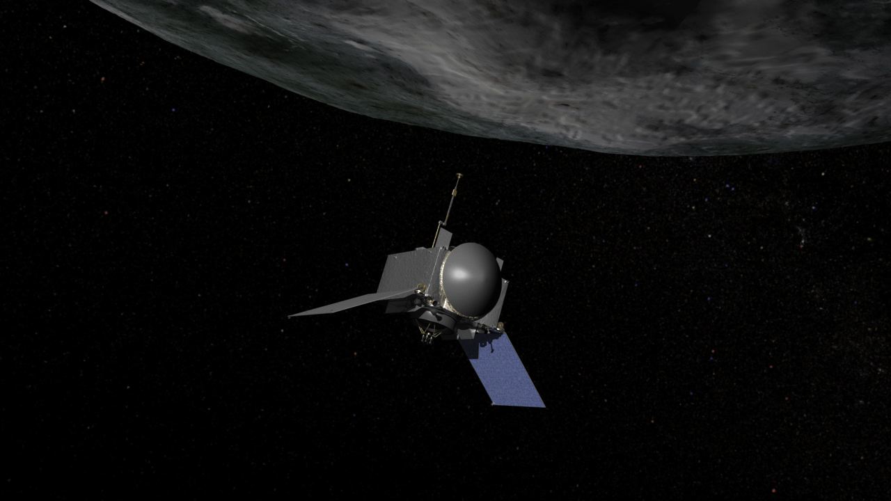
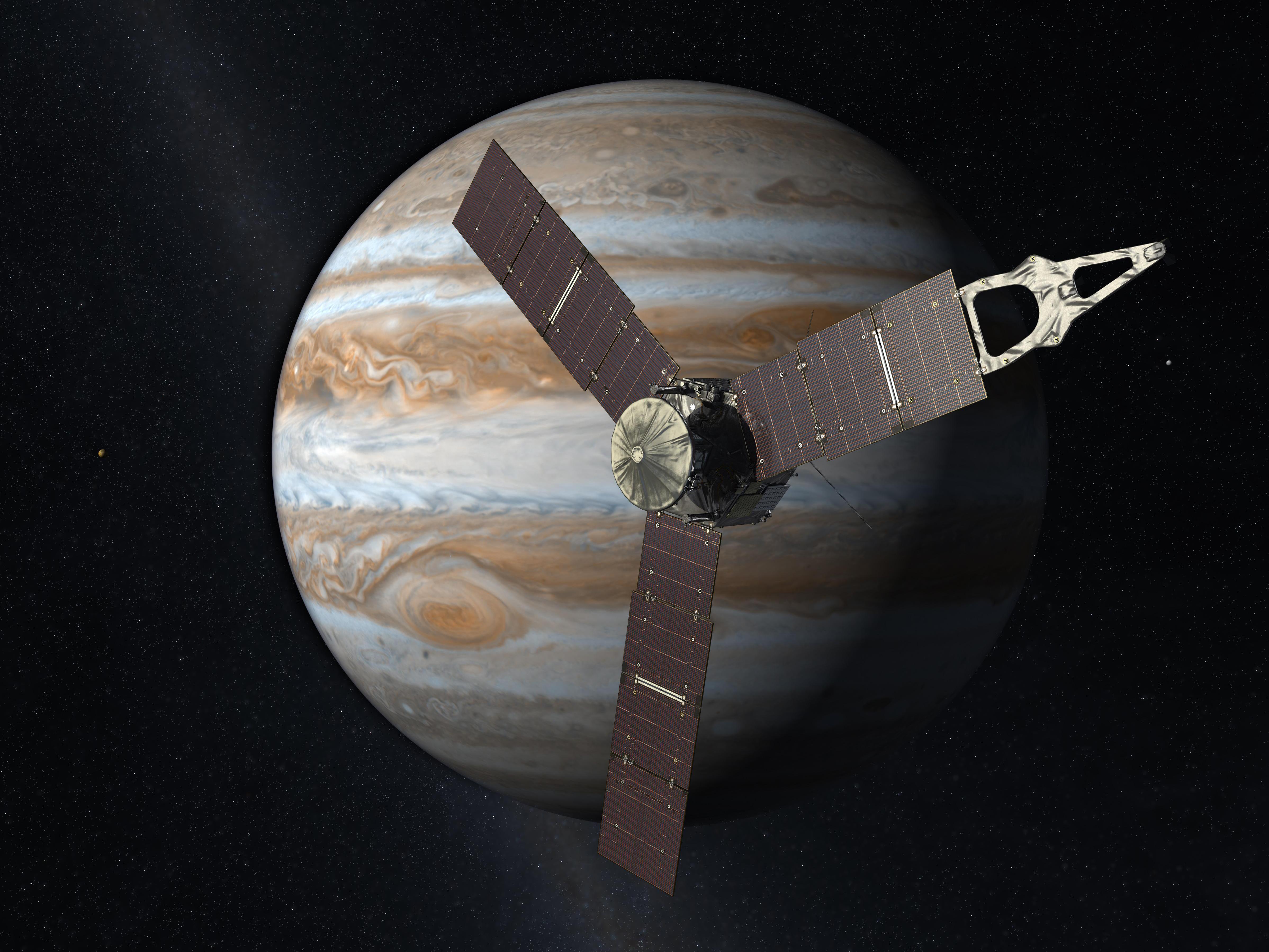
ESA Solar Orbiter: When SPARCs Fly

ESA ERC-32SC

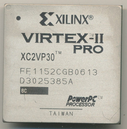
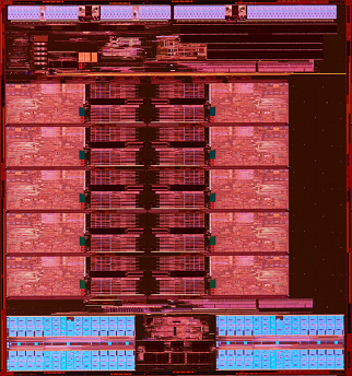
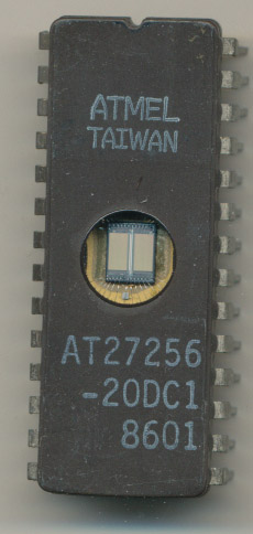
ERC-32SC – SPARC V7 MCM with RAM and MIL-STD-1553

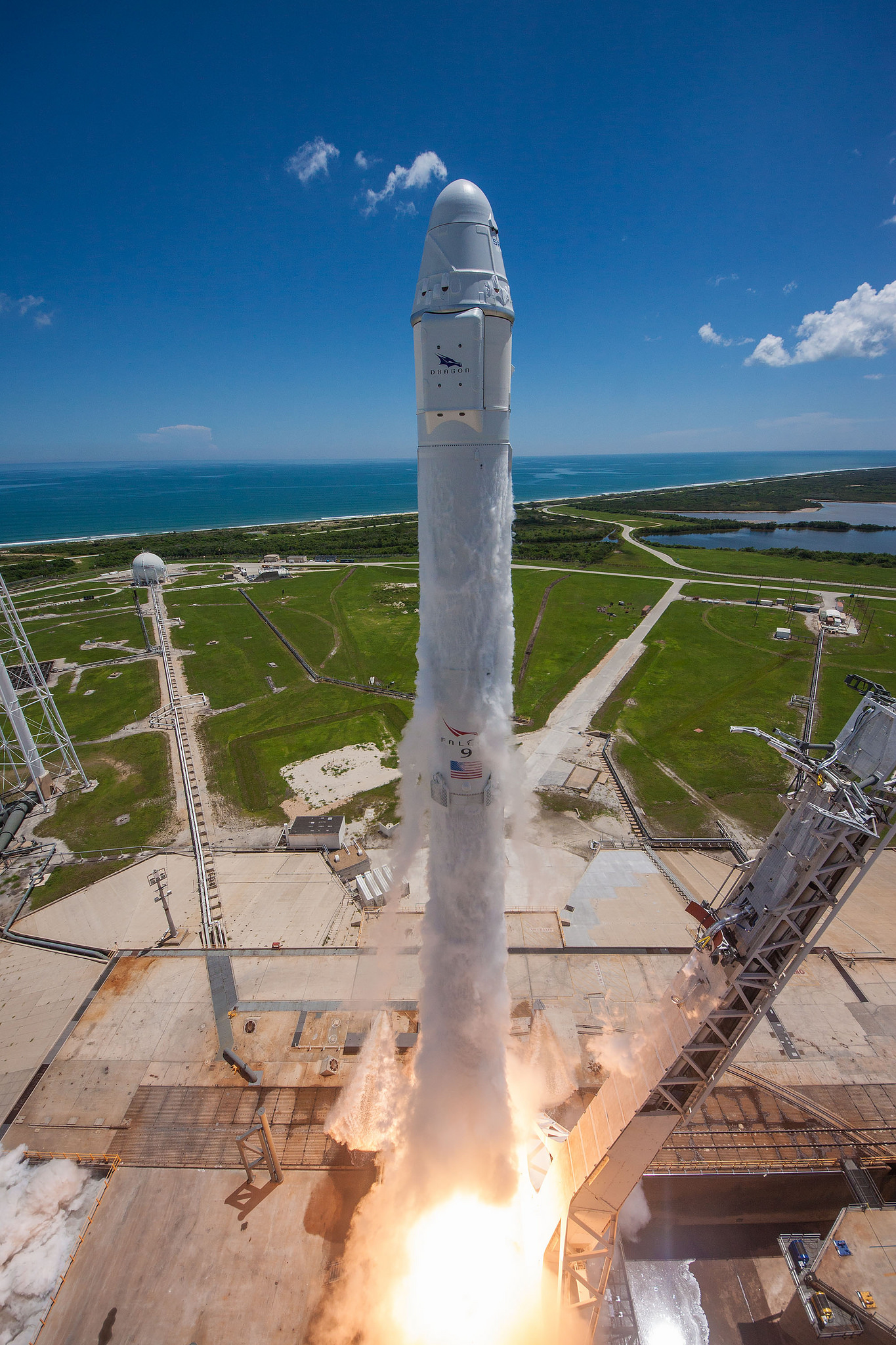
In a few hours (assuming no more delays, UPDATE: Launch Successful) the joint NASA/ESA Solar Orbiter mission will launch on a ULA Atlas 5 Rocket out of Florida, USA.  This is a mission a long time coming for the ESA, which like NASA has to get its funding from the government, except in the case of ESA, that involves the governments of many countries in the EU, which can make planning a bit more tricky.  The mission was originally baselined in 2011 and hoped to launch in…2013…then 2017..then 2018 and finally a launch date in 2020.  The original proposal dates to the late 1990’s as a mission to replace the joint NASA/ESA SOHO Solar mission that had launched in 1995.  This creates some interesting design choices for a mission, as designing often happens before a mission is completely approved/funded.  For Solar Orbiter this is one of the main reasons for it being powered by a computer that by today’s standards is rather dated, space standards no less!
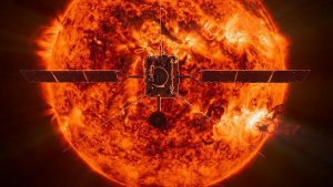
Solar Orbiter – ESA

The Solar Orbiter is powered by a processor designed by the ESA, the ERC-32SC.  This is the first generation of processors designed by the ESA.  It is a SPARC V7 compliant processor running at 25MHz and capable of 20MIPS.  The ERC-32SC is a single chip version of the original ERC-32 which was a MCM (Multi chip Module) containing 3 dies that made up the processor (the Atmel/Temic TSC691 Integer Unit TSC692 FPU and TSC693 Memory Controller) that was made on a 0.8u CMOS process.  The Single chip version was made possible by a processes shrink to 0.5u.  It was also made by Atmel,  (whom acquired Temic) and is commercially known as the TSC695 as it is designed for space use, is capable of handling a 300krad Total Ionizing Dose of radiation.  The computer used in the Solar Orbiter was built by RUAG and has two seperate ERC-32SC processor systems for redundancy.  Each of the ERC-32SCs are actually mounted on a MCM, the single chip SPARC, 48MB of DRAM (38 of which is used, the remainder is for Error Detection/Correction via Reed Solomon method), and a MIL-STD-1553 bus controller/RTC/IO are included in the package.

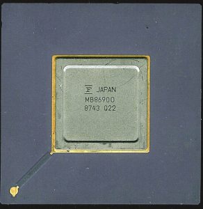
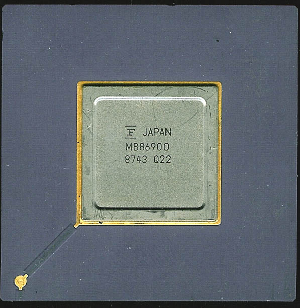
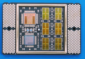
Fujitsu MB86900 – Original SPARC V7 Processor from 1987

The original specifications for this processor were developed back in the 1990’s, which is why it is a SPARC V7, equivalent to the very first Sun SPARC workstations of the late 1980’s powered by the likes of the Fujitsu MB86900/MB86901.  The ESA has developed several follow on processors since, all based on the later SPARC V8 architecture.  They are faster, and more efficient then the ERC-32SC, with some even being dual core processors.  They are known as the LEON-2 and the later LEON-3.  LEON2 has a 5-stage pipeline and no SMP support, while LEON3 increases the pipeline to 7-stages and adds SMP support.  LEON3 is also a VHDL core able to be added to many ASICS/FPGAs (LEON2 is a hard core).  The Solar Orbiter also has both LEON2 and LEON3 processors on board as well…

The Solar Orbiter caries with is 10 different scientific instruments, and each of them has their own processing subsystem, 9 of which are powered by LEON SPARC processors.  Its common for the main processor of a spacecraft to be the most powerful, but in this case the instruments each possess their own processor more powerful then that of the main spacecraft computer.   This is in large part due to many of these instruments being designed well after the original spacecraft bus and systems were baselined.  Payloads can be added/changed much later in the design of the spacecraft allowing their designers to use more modern computers.

Instrument Processor(s) Notes
Solar Orbiter OBC ERC-32SC – Atmel TSC695 Spacecraft Platform Processor
SoloHi LEON3FT – Microsemi RTAX2000 FPGA
MAG-IBS/OBS LEON3FT – Microsemi RTAX2000 FPGA
RPW-SCM/ANT LEON3FT – Microsemi RTAX4000D FPGA
LEON3FT – Cobham UT699
Two processors
SWA-HIS/EAS/PAS LEON2FT – Atmel AT697F up to 100MHz
EPD-SIS LEON2FT – IP Core
STIX LEON3FT – Microsemi RTAX2000 FPGA
EUI LEON3FT – Cobham UT699 66MHz Single core
METIS LEON2FT – Atmel AT697F
PHI LEON3FT – Cobham GR712RC Dual core up to 100MHz
SPICE 8051 + FPGA Long live the MCS-51

There is also likely more processors on this mission as well, but it can be hard to track them all down, nearly every system has its own processing (star trackers, radios/ attitude control etc)

So as you watch the launch tonight, and perhaps see science/pictures from the Solar Orbiter (or just benefit from its added help in predicting solar storms and allowing us here on Earth to prepare for them better) think of all the SPARCs it has taken to make it function.


October 12th, 2018 ~ by admin

Xilinx gets ARMed up for Free

Xilinx Virtex II Pro FPGAs from the 2000’s included embedded PowerPC processor cores.

Recently ARM announced they would be providing IP for the Cortex-M1 and M3 cores for free for users of Xilinx FPGA’s.  The Cortex-M1 and M3 are some of the most basic ARM cores, taking 12-25,000 gates for the Von Neumann architecture M1 and around 43,000 for the full up Harvard architecture M3 (with full ARM THUMB instruction set support).  Xilinx already offers FPGAs/SoCs with built in ARM cores, the SYNQ series is available with a variety of high end ARM cores such as the Cortex-A53 and the RF focused R5 core.  These obviously are fairly high gate county, and cost cores, where as the M1 and M3 cores are being provided without license, and without any royalties.  Drop in the IP into your FPGA design and go.

ARM and Xilinx say this is to meet the needs of their customers, who want to be able to use the same ARM architecture in their FPGA designs as in ASICs etc, and at the lowest investment in time and cost.  This certainly makes sense, having a free ARM core is better then a low cost ARM core, and removing the ‘paperwork’ hassle helps, but that’s probably not the only reason ARM is doing this, and doing it specifically for Xilinx.

There are a couple other things at play here, ARM Mx cores are basic RISC processors, used for when you just need to get some basic processing done, no frills, low power, and easy to use.  It turns out that’s a market that is now seeing some competition from the SiFive RISC-V core.  This is a basic, easy to use RISC core, that is synthesizable into ASICS, and FPGAs, and comes with a one time low cost license fee and no royalties.  Its being used by such heavyweights as Nvidia, and could threaten the Cortex-Mx domain, so it makes sense for ARM to offer, essentially their introductory processor core, for free, as a way to sway people to the ARM ecosystem.  But why Xilinx?

Perhaps Xilinx is just the start of ARM’s plans, Xilinx is one of the biggest providers of FPGAs in the world so certainly that will help keep people in the ARM. Xilinx infact, already has a drop-in 32-bit RISC processor core available to all their customers, the MicroBlaze and PicoBlaze, of their own design.  There are also drop in 80C186 cores, MCS-51 cores, the LEON SPARC core and many others. The other big name in FPGAs is Altera, a company that has competed with Xilinx for the better part of 30-years and was, in June of 2015 bought by none other then Intel.

Altera has had a close relationship with Intel since the 1980’s when Intel first started assisting Altera with fab’ing their PLDs.

This gave Altera greater access to Intel’s fab/engineering prowess, but also to all of Intel’s IP.  Is Intel going to offer free ARM cores on Altera FPGAs (the Stratix/Arria series does include hard Cortex-A9/A53 cores already)?  It seems unlikely that they would work to support their architectural competitor any more then they have to.  It is more likely that Intel would offer some form of 32-bit x86 processor core for their FPGAs.  Now x86 isn’t exactly known for low gate counts, but it is possible.  Currently softcore 8086 and 80186 processor (the Turbo86 and Turbo186) are 22,000 and 30,000 gates respectively, really a rounding error in FPGAs that now have millions of gates. More and more, FPGAs are becoming less FPGA like, and more ‘configurable processor’ like.

August 17th, 2017 ~ by admin

Intel Broadwell Broadens its Horizons…In Space

SpaceX CRS-12 – Carrying 116lbs of High performance Broadwell computers (image: SpaceX)

Monday’s launch of a SpaceX Falcon 9 rocket carrying a Dragon spacecraft to the space station carried what will be the most powerful computer in orbit.  In a joint project with HPE (HP Enterprise) NASA wants to test how high end computers, with off the shelf parts and construction perform in low Earth orbit.  The computer that will be soon installed is an HP Apollo 40 series (exact model is unclear, probably PC40/SX40).  It consists of 2 1U dual socket systems, running Intel Xeon E5-26xx V4 (Broadwell-EP 14nm) processors and supporting infiniband.  The only modification done was to use liquid cooling vs air cooling as the EXPRESS racks on the ISS are not set up to handle the heat load the computer generates.  The computers run on a standard 110VAC supply, provided by a NASA supplied inverter, which takes the 48VDC power generated by ISS’s solar arrays and converts it to the 110VAC needed by the Apollo computer.

The Broadwell processors are made on a 14nm process, and are some of the latest made by Intel (NASA froze the design in March so they were the fastest available to HPE at that time).  Performance will be just over 1Teraflop, a great increase over the main computers that actually RUN the ISS, which are Intel 80386SX based.  The astronauts themselves use laptops of various pedigrees, mainly Lenovo Core 2 Duo based A61Ps (these are being replaced by HP Zbook 15s powered by Intel 7th Gen Core i5 and i7 processors) , so the Apollo is a great leap up from them as well.

Mockup of HPE Apollo Computers for EXPRESS rack integrations. 2 computers with water cooling system between them.

To test the Apollo, NASA will run an identical system on the ground, performing the same tasks, and compare the outputs.  They want to see how the computers handle the environment in space, with various loads and electrical conditions.  One computer (both on the ground and on the ISS) will be run at maximum performance for the entirety of the experiment, while the other will have its computing/electrical load dynamically varied.

Radiation is usually one of the biggest concerns for space based computers, but on the ISS, radiation levels are not particularly high.  Daily doses experienced by the crewmembers are in the 10-50 millirad range. There are of course periods of higher radiation, either from where the ISS is in orbit, or from space weather.  The water cooling will further shield parts of the computer from radiation (water being a great radiation shield).  The Broadwell-EP processors have around 7.2 billion transistors, increasing the

10-core Broadwell die. Made on 14nm process.

chance that even a small amount of radiation may have an effect.  By running one set of computers at maximum performance, NASA can see these effects quickly.  Does the performance decrease? Does the power draw start spiking? Or is data being lost in the Infiniband networking PCIe card?

Currently experiment data has to be transferred to the ground in raw unprocessed format, as nothing on the ISS can handle the computing need to process it.  If the high performance computing experiment is successful, it can give the astronauts the ability to do processing and analysis of experimental data in orbit,. and transfer only the results to the ground, saving precious bandwidth, and allowing for experiments to be modified, changed, or created in orbit based on the ongoing results.


More Information: 

NASA: HPC COTS Experiment

HPE: The space station gets a new supercomputer

Tags:
,

Posted in:
Processor News

September 13th, 2016 ~ by admin

OSIRIS-REx: Bringing Back Some Bennu

OSIRIS-Rex: RAD750 to Bennu

OSIRIS-Rex: RAD750 to Bennu

The Apollo Group  carbonaceous asteroid Bennu is a potential Earth impactor, with a 0.037% likelihood of hitting earth somewhere between 2169 and 2199.  Bennu is thought to be made of materials left over from the very early beginnings of our solar system, making researching them a very tantalizing proposition.  Rather than wait for the small chance of Bennu delivering a sample to Earth in 150 years the thoughtful folks at NASA decided to just go fetch a bit of Bennu.  Thus is the mission of OSIRIS-REx which was launched a few days ago (Sept 8, 2016) aboard an Atlas V 441 as an $850 Million New Frontiers mission.

Somewhat surprisingly there is scant details about the computer systems that are driving this mission to Bennu.  OSIRIS-REx is based on the design of the Mars Reconnaissance Orbiter (MRO), MAVEN and Juno, and thus is based on the now ubiquitous BAE RAD750 PowerPC processor running the redundant A/B side C&DH computers.  This is the main ‘brain’ of the Lockheed Martin built spacecraft.  Of course the dual RAD750s are far from the only processors on the spacecraft, with communications, attitude control, and instrumentation having their own (at this point unfortunately unknown) processors.

REXIS Electronics: Virtex 5QV - Yellow Blocks are Off the Shelf IP, Green Blocks are custom by the REXIS Team. Powered by a Microblaze SoftCore.

REXIS Electronics: Virtex 5QV – Yellow Blocks are Off the Shelf IP, Green Blocks are custom by the REXIS Team. Powered by a Microblaze SoftCore.

One instrument in particular we do know a fair amount about though.  Regolith X-ray Imaging Spectrometer (REXIS) is a student project from Harvard and MIT. REXIS maps the asteroid by using the Sun as an X-ray source to illuminate Bennu, which absorbs these X-rays and fluoresces its own X-rays based on the chemical composition of the asteroid surface. In addition REXIS also includes the SXM, to monitor the Sun’s X-Rays providing context to what REXIS is detecting as it maps Bennu.  REXIS is based on a Xilinx Virtex-5QV Rad-Hard FPGA.  This allows for a mix of off the shelf IP blocks, and custom logic as well. The 5QV is a CMOS 65nm part designed for use in space.  Its process, and logic design are built such as to minimize any Single Event Upsets (SEU), and other radiation induced errors.  It is not simply a higher tested version of a commercial part, but an entirely different device.   Implemented on this FPGA is a 32-bit RISC softcore processor known as Microblaze.  The Microblaze has ECC caches implemented in the BRAM (Block RAM) of the FPGA itself and runs at 100MHz.

It will take OSIRIS-REx 7 years to get to Bennu, sample its surface, and return its sample to Earth.  By the time it gets back, the RAD750 powering it may not be so ubiquitous, NASA is working on determining what best to replace the RAD750 with in future designs.  Currently several possibilities are being evaluated, including a QuadCore PowerPC by BAE, a QuadCore SPARC (Leon4FT), and a multi-core processor based on the Tilera architecture.  As with consumer electronics, multi-core processors can provide similar benefits in space of hogher performance and more flexible power budgeting all with the added benefit (when design for such) of increased fault tolerance.

July 3rd, 2016 ~ by admin

Juno Joins Jupiter: And Brings Some Computers For The Trip

Juno - RAD750 Powered Mission to Jupiter

Juno – RAD750 Powered Mission to Jupiter

NASA’s Juno mission to Jupiter arrives in just about a day, after a 5 year journey that began in August of 2011 aboard an Atlas V rocket.  The Juno mission is primarily concerned with studying the magnetic fields, particles, and structure of Jupiter.  Finding out how Jupiter works, and what its core is made of are some of Juno’s goals.  None of the experiments need a camera, but NASA decided, in the interest of public outreach and education, that if you are going to spend $1 billion to send a probe to Jupiter, it probably should have a camera.  Energetic particle detectors, Magnetometers, and Auroral Mappers are great for science, but what the public is inspired by is pretty pictures of wild and distant worlds.

Juno is powered by a now familiar computer, the BAE RAD750 PowerPC radiation hardened computer.  It operates at up to 200MHz (about the processing power of a mid 1990’s Apple Computer) and includes 256MB of Flash memory and 128MB of DRAM.  It (and the other electronics) are encased in a 1cm thick titanium radiation vault.  Flying in a polar orbit around Jupiter, Juno will experience intense radiation and magnetic fields.  The probe is expected to encounter radiation levels in the order of 10Mrads+.  The vault limits this to 25krads, within what the electronics can handle.  It should be noted that a dose of 10krads is fatal in most cases.  This intense of radiation will degrade the prober, even with shielding, resulting in a mission life of only 37 orbits (a little over a year) before the probe will be gracefully crashed into Jupiter.

Read More »

June 21st, 2016 ~ by admin

Fujitsu to take ARM into the realm of Super

Fujitsu MB86900 - Original SPARC Processor from 1987

Fujitsu MB86900 – Original SPARC Processor from 1987 – 14.28MHz

Back in 1987 Fujitsu was one of the founders of the SPARC RISC architecture.  The very first SPARC processors were built by Fujitsu, and used in their servers through the 1990’s and 2000’s. SPARC processors were first used in the CM-5 Thinking Machine in 1991 using 1024 SPARC processors (later upgraded to SuperSPARCs).  Fujitsu began making supercomputers based on SPARC in 1992 with the AP1000 and its UltraSPARC based successor the AP3000.  One of their latest, the K machine, is a 705,024 core 12MW SPARC64 VIIIfx based design that ranks as #5 on the Top 500 Supercomputer list.

This is why its a surprise to many that they have announced the successor to the K Machine will be similar in topology, and will be RISC based, but will not be SPARC based, rather Fujitsu has been working with another well known RISC architecture with serious HPC aspirations, ARM.  Fujitsu has been an ARM architecture license holder for some time and the post-K machine will be based on the 64-bit ARMv8 architecture.  ARM has been working hard to make their chips appeal to the datacenter environment, with some success.  Their low power consumption makes them ideal for high density applications, which a super computer needs.  Estimated performance is 1,000 Peta FLOPS and it is due to go into service in 2020. A speed that would eclipse another recently announced RISC supercomputer….

Read More »

Posted in:
Processor News

February 3rd, 2016 ~ by admin

The End of the Omega

ST STi5500 - The Original 50MHz Transputer based Omega

ST STi5500 – The Original 50MHz Transputer based Omega

In January ST announced that they would be exiting the Digital Set Top Box (STB) market.  This is a market that they arguably led for the last 20 years, and one that really began with their Omega processor in 1997. The ST Omega processor line, beginning with the STi5500 powered set top boxes, for cable companies, satellite companies, and DVR’s as well as other TV connected devices.  Open up a satellite TV receiver from the last 20 years and you are very likely to find a STi Omega chipset.

The STi5500 was the beginning, and interestingly at its core was a ST20 processor, based on the Inmos Transputer (which ST now owned) from the late 1980’s.  The Transputer was meant to revolutionize computing, making processors so cheap, that they could be embedded into pretty much any other logic device, what today we call an SoC, but in 1985, was a novel idea.  At the time it didn’t really succeed, but ended up seeing its intended use 10+ years later in the Omega.  In the 1980s the Transputer saw speeds of up to 30MHz, int he STi5500 it ran at 50MHz with 2K of I-cache + 2K of Data Cache as well as 2K of SRAM that could be used as data cache.

ST STi5514 - Enhanced 180MHz Omega

ST STi5514 – Enhanced 180MHz Omega

In the early 2000s the Omega was upgraded to a faster ST20 core, eventually hitting 243MHz in the STi5100, now with the caches increased to 8K each, as well as 8K of SRAM.  This was getting to be the limit of the ST20 Transputer core.  ST needed a core that could support higher speeds running such things as Java and Windows CE amongst other things, as well as support the higher resolutions and audio quality requirements.

ST handled this is in two entirely different ways.  First they licensed the SH-4 32-bit RISC core from Hitachi, a rather surprising move but STBs was not a market Hitachi was in, so it was in both companies best interest.  ST also was working on their own new core to replace the ST20, and they had help, from a very surprising partner.

Read More »

January 21st, 2016 ~ by admin

Microchip PIC’s up Atmel

Microchip PIC16C62 ENG SAMPLE - 1989

Microchip PIC16C62 ENG SAMPLE – 1989

Yesterday Microchip, makers of the PIC line of microcontrollers, announced they were buying Atmel, for a cool $3.56 Billion.  This isn’t entirely surprising considering the ongoing consolidation in the industry, It was only last year that Dialog attempted to purchase Atmel, and before that ON Semiconductor and Microchip. In December of 2015 NXP and Freescale (formerly Motorola Semiconductors) merged, creating one of the largest microelectronics companies.  These mergers do create an interesting result, product mixes that were formerly competitors, end up being marketed side by side.  In the case of NXP and Freescale, NXP marketed many MCS-51 microcontrollers in their 8/16-bit lines, while Freescale of course sold many versions of MC6800 based MCU’s.  These two rivalries have existed since the early 1980’s and likely will continue.  Perhaps the biggest rivalry in MCU though is between Atmel and Microchip.

Atmel EPROM, fab'd by GI in 1986, right before they became Microchip

Atmel EPROM, fab’d by GI in 1986, right before they became Microchip

Microchip was spun off of General Instrument in 1987, but the PIC architecture dates back to 1976, and is still being made in nearly the same form (PIC16C55).  Atmel was started in 1984, first making EPROMs, and then MCS-51 microcontrollers, one of the very first companies to make an 8051 with on die flash memory.  In a bit of a twist of fate, when Atmel started, it was a fabless company, it contracted with several companies to make its EPROMs, including Sanyo, and General Instruments, which as mentioned above, became Microchip.  Atmel also makes APRC processors, and for a time made Motorola products as well (Atmel has a very convoluted history, for more info on this read here and here )

Today the PIC line continues to be popular, with devices for the low end, such as the PIC10/12 all the way to the MIPS based PIC24 on the upper end.  Atmel continues to make 8051 MCUs, but also makes the 8 and 32-bit AVR line, perhaps best known today for its use in Arduino boards.  They also make MCU’s based on the ARM core, a competitor to MIPS, and Atmel’s own AVR32.

Likely to the consternation to many fans of either company, this merger does make sense, more so than ON or Dialog buying Atmel.  While Microchip and Atmel both compete in the same markets, they do so with different architectures.  Product lines are unlikely to change, and overhead saving should free up $$ both for stockholders (yawn) and engineering teams alike. No word has been giving yet on wether Microchip intends to keep the Atmel branding, but perhaps they should, as an AVR MCU with a Microchip logo on it may just prove to be too much for some.

April 9th, 2015 ~ by admin

The e2v PowerPC and HiTCE Packages

Atmel PC7410MGH450LE - Motorola Marked Package

Atmel PC7410MGH450LE – Motorola Marked Package – 2003

In the 1970’s second sources were quite important in the processor industry.  They provided a stable supply of a designed in part if the primary manufacturer (which often only had a fab or 2) had problems.  They also could widen the market for the processor.  Many of these agreements were kept active for decades after, resulting in some interesting results.

Motorola licensed many of their design to SGS, which later merged with Thomson to become STMicroelectronics. though the Thomson name was still used.  Thomson license built most of Motorola’s product line, as well as many high reliability versions.  In 1999 Atmel bought Thomson-CSF Semiconductors, and continued to make Motorola products (in their Grenoble France fab), which now included Motorola’s PowerPC line as well as the 68k line of processors.  This portion of Atmel was sold to e2v (in England) in 2006, which continued to produce the Motorola (now spun off as Freescale) PowerPC line, now branded as e2V.

The packaging used by e2v (and previously Atmel) is the same as that used by Motorola/Freescale.  The packages were custom made for Motorola/Freescale by Kyocera (and others) and so often chips with both Atmel/Motorola and e2v/Freescale markings can be found.  It is this packaging that is of interest, as it shows an interesting aspect of processor design.

Read More »

March 11th, 2015 ~ by admin

Emulating the Intel 8080 on a MOS 6502

Pagetable.com has in interesting post about emulators, specifically one created in 1978 to run Intel 8080 code on a 6502.  While emulators today are fairly common, such as running Nintendo (6502) games on a PC, or In Circuit Emulators for development, an 8-bit cross architecture emulator is certainly different.  Especially since the 8080 and 6502 were so vastly differing.  Certainly a useful tool for teaching oneself a new architecture, and as they were coming out rather rapidly in the 1970’s knowing more then one was a worthy investment.

Todays equivalent perhaps would be emulating a PIC on a 8051.  Perhaps someone will give it a try?

Tags:
,

Posted in:
Processor News