February 11th, 2022 ~ by admin

How do you test a S3 GPU? With an HP 93000

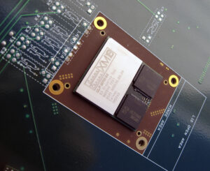
GammaChrome XM18 – Engineering Sample

Recently I got in some very nice S3 GammaChrome GPUs.  The GammaChrome was S3 (owned by VIAs) follow on to the DeltaChrome and included support for such things at PCI-E.  The S18 (Code name Brooklyn) supported speeds of up to 500MHz and was made on a 130nm process by TSMC.  S3 also made a mobile version of the S18 called the XM18 (Code name Metro MPM) in 64MB and 32MB versions.  Clock speed on these was around 350MHz (memory on the samples I have is 350 so core should be similar).  The XM18 was packaged on a MPM (Multi Package Module) with 2 RAM chips and the GPU mounted on a small chip size BGA with around 800 balls.  This is very similar to how ATI packaged some of their mobile GPUs (like the Mobility Radeon 7500 and 9600).

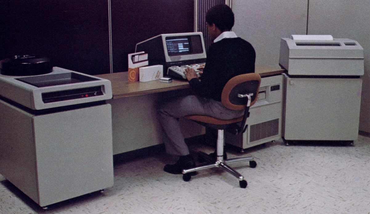
HP 93000 (from HP Brochure)

So how do you test one of the XM18 Engineering Samples? Or any large scale chip for

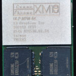
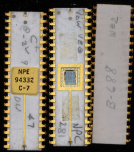
86C813 ES Gamma Chrome XM18 ULP MPM64

that matter?  With Automated Test Equipment.  ATE systems are designed to rapidly test various chips to verify their design/performance before they go into full production (or to test samples of production ones).  The HP/Agilent 93000 (spunoff as Verigy in 2007 and acquired by Advantest Corporation in 2011) was introduced in 1999 to handle such testing, and at the time was rather revolutionary.  Previously most test systems used a simple test head that would mount the chip to be tested, with all the processing and customizations being contained in the main test machine.  This worked fine for a single design, but to test multiple chips got pretty expensive.  HP moved the testing to the test head directly, interfacing to the target chip via a large PCB.  This way changing chips only required updating the test program, and changing out the PCB.  Design changes required reworking a single PCB, rather then the entire test machine.

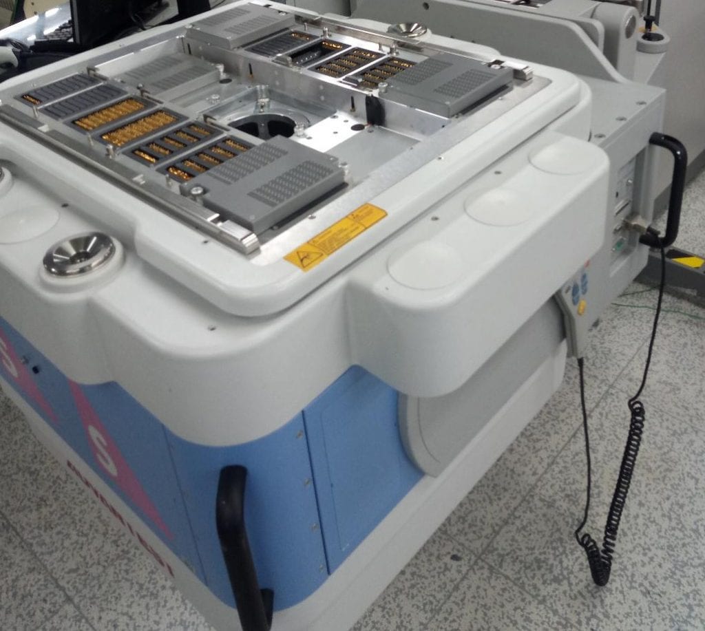
HP 93000 Test Head – Notice the 16 groups of pins (some covers and some mangled in this old sale photo)

The 93000 was the first ATE that achieved (on its low end (200Mbps) a cost of $1000/pin tested, and on the high end, test speeds of up to 1250Mbps (for the P1000 version, at a cost of $6-7000 per pin).  The XM18 has around 800 pins, half are probably power/ground so 400 some odd testable pins, in a mid range HP 93000 and you see these systems were not inexpensive. Well over a million dollars for a midrange system.

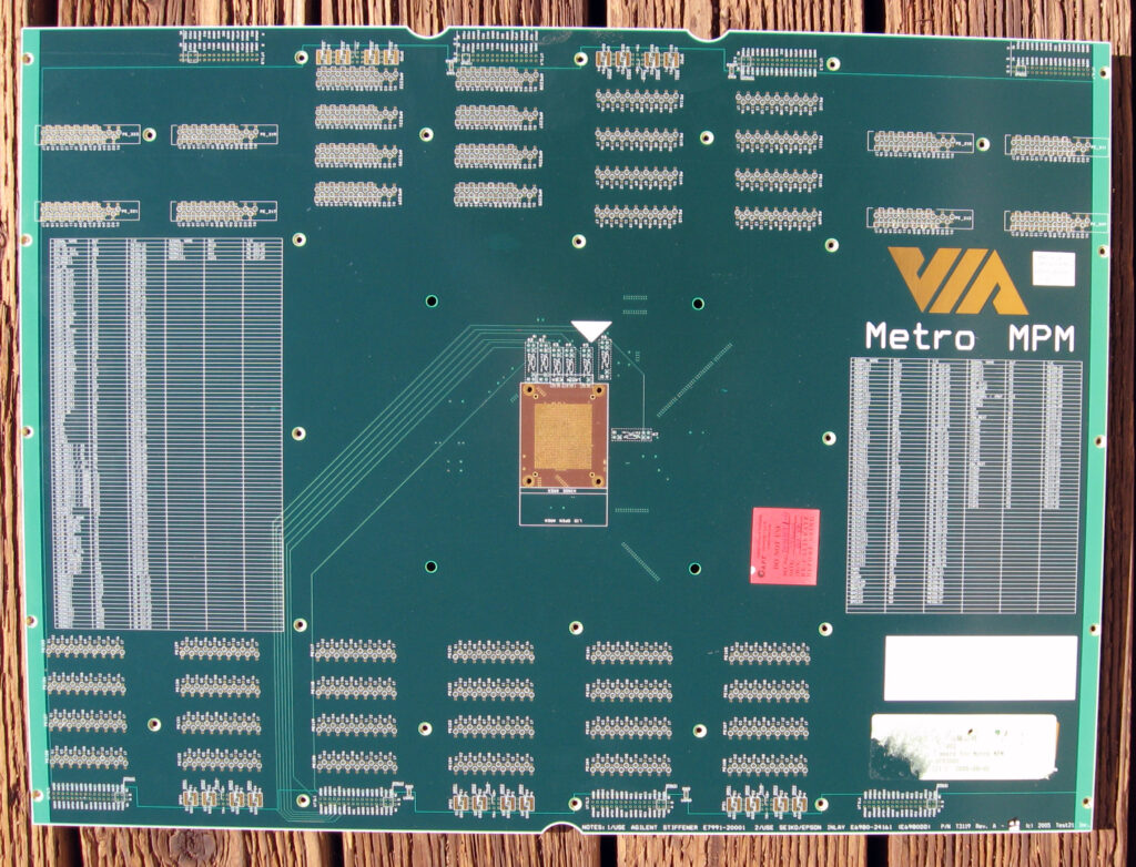
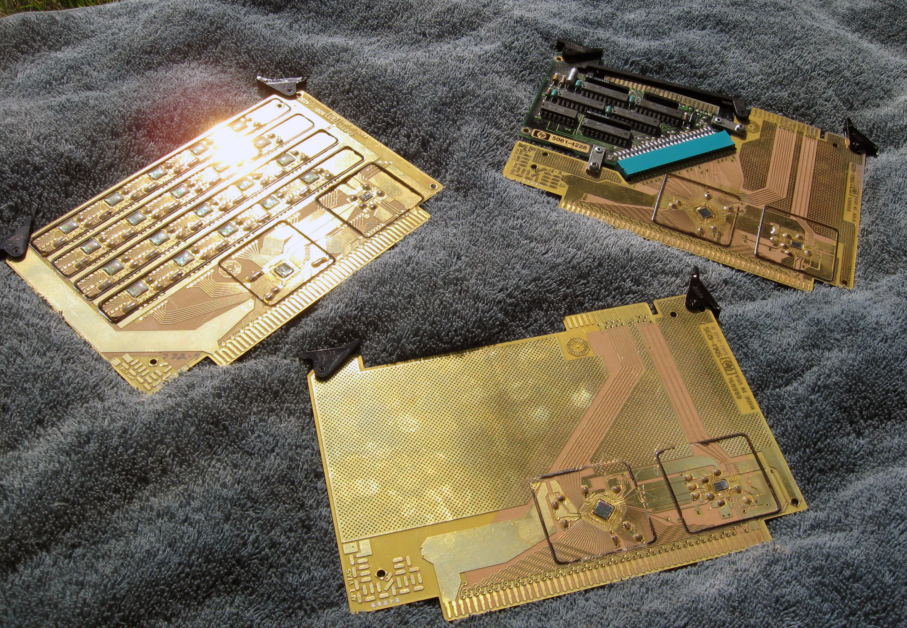
GammaChrome XM18 – Metro MPM Test Board

To use such a system the chip to be tested would be mounted on the test board, usually with a BGA socket.  This board breaks out all the various connections of the chip to 16 sets of contacts, which the probe head of the HP 93000 made contact with using spring loaded contacts.  The board is then clamped down and tests are run.

Connection List

These boards are very very large, each one is 17x23inches (43x58cm) and 5mm thick.  They weigh about 7lbs (3.1kg) as well.  They got used a lot and need to be rather robust and durable.  You can see the boards are marked with tables of all the connections, and where they are brought out to.  Useful information about what supporting equipment is need (sockets and stiffeners etc) is marked on the board as well.

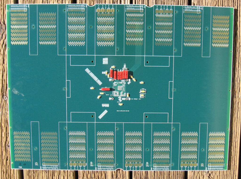
Back of board. Notice all the capacitors, a crystal, and a series of 5VDC reed relays (the red devices)

These boards appear to be a ‘static’ type item, but they do require adjustment, notice the markings that say not to use this board, it needs recalibrated.  Looking closely at the board you can see capacitors have been removed/replaced, and many of the capacitors have felt tip marker markings on them.  Keeping the capacitance and inductances at their proper values 9and matched, considering the long trace lengths) would be a very important thing.

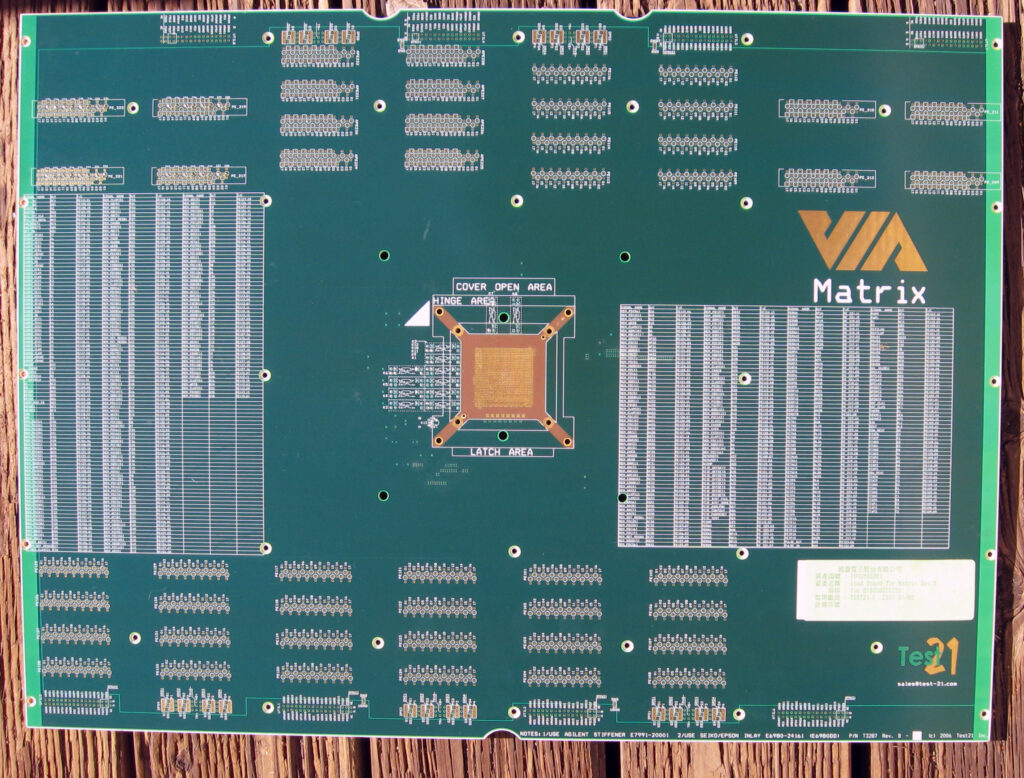
S3/VIA Matrix Test Board. The Matrix was the code name for the GammaChrome S14/S19

These test boards are from 2006, the 93000 systems are still being used today in upgraded form (now called the V93000) to test SoCs and other chips.  As chips have gotten more and more complex, faster, and with larger pin outs, test equipment continues to grow ins peed, and cost as well, but is an essential part to the process of designing, producing and supporting a successful GPU or CPU.

Tags:
, , ,

Posted in:
Boards and Systems

August 9th, 2020 ~ by admin

The Forgotten Ones: HP Nanoprocessor

Original Nanoprocessor prototypes from 1974-75. Note hand written wafer number, open die cover and early part number (94332)

Back in the 1970’s the Loveland Instrument Division (LID) of HP in Colorado, USA was the forefront of much of HP’s computing innovation.  HP was a leader, and often THE leader in computerized instrumentation in the early 1970’s.  From things like calculators, to O-scopes to desktop computers like the 9825 and 9845 series.  HP made their own processors for most all of these products.  The early computers were based on the 16-bit Hybrid processor we talked about before.  At around the same time, in 1974, the HP LID realized they needed another processor, a control oriented processor that was programmable, and could be used to control the various hardware systems they were building.  This didn’t need to be a beast like the 16-bit Hybrids, but something simpler, inexpensive, and very fast, it would interface and control things like HPIB cards, printers, and the like.  The task of designing such a processor fell to Larry Bower.

The result was a Control Oriented Processor called the HP nanoprocessor.  Internally it was given the identifier 94332 (or 9-4332), not the most elegant name, but its what was on the original prototypes and die.   The goal was to use HP’s original 7-micron NMOS process (rather then the new 5-micron NMOS-II process) to help save costs and get it into production quickly.

Nanoprocessor Features – Note the speed has been ‘adjusted’


The original design goal was a 5MHz clock rate and instructions that would execute in 2 cycles (400ns).  The early datasheets have this crossed out and replaced with 4MHz and 500ns, yields at 5MHz must not have been high enough, and 4MHz was plenty.

Handwritten Block diagram


The Nanoprocessor is interesting as it is specifically NOT an arithmetic oriented processor, in fact, it doesn’t even support arithmetic.  It has 42 8-bit instructions, centered around control logic.  These are supported by 16 8-bit registers, an 8-bit Accumulator and an 11-bit Program Counter.  Interface to the external world is via an 11-bit address bus, 8-bit Data bus and a 7-bit ‘Direct Control’ bus which functions as an I/O bus.  The nanoprocessor supports both external vectored interrupts and subroutines.  The instructions support the ability to test, set and clear each bit in the accumulator, as well as comparisons, increments/decrements (both binary and BCD), and complements.

Here is one mask (Mask 5 of 6) for the prototype Nanoprocessor. You can see its simplicity.  On the bottom of the mask you can see the 11-bit address buffers and Program Counter

2.66MHz 1820-1691 – note the -5V Bias Voltage marked on it

The Nanoprocessor required a simple TTL clock, and 3 power supplies, a +12 and +5VDC for the logic and a -2VDC to -5VDC back gate bias voltage.  This bias voltage was dependent on manufacturing variables so was not always the same chip to chip (the goal would be -5VDC).  Each chip was tested the and voltage was hand written on the chip.  The voltage was then set by a single resistor on the PCB.  Swapping out a Nanoprocessor meant you needed to make sure this bias voltage was set correctly.

If you needed support for an ALU you could add one externally (likely with a pair of ‘181 series TTL).  Even with an external ALU the Nanoprocessor was very fast.   The projected cost of a Nanoprocessor in 1974 was $15 (or $22 with an ALU),  In late 1975 this was $18 for the 4MHz version  (1820-1692) and $13 for the slower 2.66MHz version (1820-1691).

At the time of its development in 1974-1975 the Motorola 6800 had just been announced. The 6800 was an 8-bit processor as well, made on a NMOS process, and had a maximum clock rate of 1MHz.  The initial cost of the 6800 was $360, dropping to $175, then $69 with the release of the 6502 from MOS.  By 1976 the 6800 was only $36, but this is still double what a Nanoprocessor cost


An early ‘slide deck’ (the paper version equivalent) from December 1974 sets out the What Why and How of the Nanoprocessor.  The total cost of its development was projected to be only $250,000 (around $1 million in 2020 USD).  The paper compares the performance of the Nanoprocessor to that of the 6800.  The comparisons are pretty amazing.

Interrupted Count Benchmark

For control processing interrupt response time is very important, the Nanoprocessor can handle interrupts in a max of 715ns, compare that to 12usec for the 6800.   The clock rate of the Nanoprocessor is 4 times faster but the efficiency of its interrupts and instructions are what really provides the difference here.

The clock rate difference (1MHz vs 4) really shows here, but the Nanoprocessor is also executed 3 times the instructions to do the same task, and still is faster.

Even using an external ALU compared to the Motorola’s internal ALU, the nanoprocessor is better then twice as fast (thanks here to its much higher clock frequency)

Full Handshake Data Transfer. Interfacing to the outside world was the main driver of the Nanoprocessor. Here we see that it can ‘talk’ to other devices much faster then the 6800

All instructions on the Nanoprocessor take 500ns to execute compared to the 1-10u for the 6800.

Today we do benchmarks based on framerates in games, or render times, but you can see that benchmarks were even important back then.  How fast a processor could handle things determined how fast the printer could be, or how fast it could handle external data coming in.  It’s no wonder that the Nanoprocessor continued to be made into the late 1980’s and many of them are still in use today running various HP equipment.

Nanoprocessor User Manual – October 1974

A big thank you to Larry Bower, the project lead and designer of the Nanoprocessor, who donated several prototypes, a complete mask set, and very early documentation on the Nanoprocessor (amongst some other goodies)

Documentation so ealy it has many hand written parts, and some corrections.  This had to be a very annoying oops if it wasn’t caught early on.  Even Engineers get their left and right mixed up on occasion


Posted in:
CPU of the Day

August 25th, 2018 ~ by admin

CPU of the Day: FOCUS on 32-bits

1983 HP FOCUS Board set – Pre FPU. Top left: Memory. Top Right: I/O and CPU bottom center

The year is 1981, Intel is making the 8/16-bit 8086/8088, and Motorola has released the 16/32-bit 68000 processor to much fanfare.  Motorola marketed this as the first 32-bit processor, but while it supports 32-bit instructions/data it does so with a 16-bit ALU.  HP, always used the MC68000 in their 9000 Series 200 line of computers, providing rather good performance for 1981. But this was the 1980’s and HP wasn’t satisfied with good, they wanted more, they wanted to implement a full 32-bit computer on something less then the 5,000 IC’s typically used to implement one at that time.  This meant making a processor like nothing else before, something with more then the 68,000 transistors of the MC68000 or even the 134,000 transistors of the new i286 Intel had announced.  What HP made is simply remarkable, in 1981 they announced the HP 9000 Series 500 computers, powered by an all new fully 32-bit processor called the FOCUS.  FOCUS was made on HP’s high density NMOS-III process, a 1.5u process, and used 450,000 transistors.  Thats 450,000 transistors on a single 40.8mm2 piece of 1.5u silicon in 1981, a smaller die than the Intel 286.

Read More »

Tags:
, ,

Posted in:
CPU of the Day

January 28th, 2018 ~ by admin

CPU of the Day: Tandem CLX 800 – It Takes 2 To Tango

TANDEM CLX 800 Processor – VLSI CMOS 1u process – 16MHz.

Tandem Computers was established way back in 1974, and was one of the first (if not the first) dedicated fault-tolerant computing companies.  They designed completely custom computers designed for use in high reliability transaction processing environments.  These were used for support of stock exchanges, banks, ATM networks, telephone/communications interchanges, and other areas where a computer failure would result in significant, costly, disruptions to business services.  Tandem was started by James Treybig, formally of HP, and a team he lured away from HP’s 3000 computer line.

Tandem computers are designed to do two things well, fail-over quickly when a failed part is detected.  This means that if a faulty processor or memory element is found, it can be automatically disabled, and processing continues, uninterrupted, on the rest of the system.  The other design element that Tandem perfected was allowing the computer to find and isolate intermittent problems.  If a processor or storage element ceases to work, that is relatively easy to figure out, but if a processor is glitchy, causing errors only occasionally, that can be much harder to find and can result in serious problems for the user.  This is known as ‘Fast Fail’ and today is a pretty standard concept, find the error, catch it, and prevent erroneous data from ever making it back into the database.  Tandem computers were designed from the ground up to be fault tolerant, disks were mirrors, power supplies, busses,

Tandem CLX 600 PCB (click for larger)

processors,all were redundant, but unlike some other systems, components were not kept as ‘hot spares’ sitting idle until something failed.  This kept hardware from being ‘wasted.’ Under normal operation if it was in the system, it was contributing to system performance.  A failed component then would reduce system performance until it was replaced/fixed, but a customer would not be paying for hardware that served them no purpose unless something broke.

To support these goals Tandem designed their own processors and instruction set architecture know as TNS (Tandem NonStop).  The first processors were a 16-bit design call the T/16 (later branded NonStop I) made out of TTL and SRAM chips spanning 2 PCBs.  Performance was around 0.7MIPS in 1976.  They were a stack based design similar to the HP3000 with added registers as well.  T/16 systems supported 2-16 processors. NonStop II, released in 1981, was similar, but supported the occasional 32-bit addressing, increasing accessible memory form 1 to 2MB per CPU and performance to 0.8MIPS.

The 1983 introduction of TXP saw a great performance improvement, up to 2.0 MIPS, but kept the same form factor.  The processor was implemented in TTL, with the addition of many PALs and added much better support for 32-bit addressing.  In 1986 the NonStop VLX was released, which moved to an ECL based processor.  This was a full 32-bit design, running at 12MHz (3MIPS) but still using discrete components and a new bus system as well.  This was to be the high end of the NonStop line, it was fast reliable, and rather large.  The desire for a more economical system to fit the needs of smaller customers led to a first for Tandem…

Read More »

Posted in:
CPU of the Day

January 15th, 2017 ~ by admin

HP 1000 A700 Processor: Rise of the Phoenix

HP 12152-60002 A700 Phoenix Processor – 4x AMD AM2903 (1820-2377)

The Lighting processors of the HP A600 and A600+ were good performing for 1982.  They filled the entry and mid range slots of the HP 1000 A Series quite well.  The additional floating point support of the A600+ in 1984 helped considerably as well, but what was needed for truly better performance on the high end was hardware math support.  While the HP A600 took only 9 months to design and release, the A700, released at the same time, took somewhat longer.  The A600 was based on the AMD 2901, which had been released way back in 1975.  The A700 Phoenix was based on its successor, the AM2903.  The 2903 added a few important features to the bit-slicer.  Hardware multiply and divide support,support for more registers, and easier ways to access them, and parity generation.  This is why the A700 took longer to design, the A600 design was begun half way through the A700 to fill the lower end, where the features of the 2903 wouldn’t be as missed.

The A700 performs at the same 1 MIPS as the A600 but supports 205 standard instructions (compared to 182 for the A600 and 239 for the A600+).  It adds more register reference instructions, dynamic  mapping, I/O and more math based instructions.  Cycle time is actually slightly slower, 250ns compared to 227ns for the A600 but the 2903 allows more efficiency making up for the difference.  A typical FMP instruction take 13.75-25.25 microseconds compared to 16.6-26.6 on the 2901 powered A600.  This is a direct result of the hardware multiply hardware included in the 2903.  The A600+, with its faster 2901C’s completes the same instruction in 17-21.1 microseconds, FASTER then the A700. But the A700 has a trick up its sleeve….

Read More »

Tags:
, , , ,

Posted in:
CPU of the Day

November 26th, 2016 ~ by admin

HP 3000 Series 33: 16-bits of Sapphire

HP 3000 Series 33 - 16-bits 11MHz. They were integrated into the desk, with a 20MB hard drive on the left, and the computer on the right (with a 1.2MB 8" Floppy Drive)

HP 3000 Series 33 – 16-bits 11MHz. They were integrated into the desk, with a 20MB hard drive on the left, and the computer on the right (with a 1.2MB 8″ Floppy Drive)

In 1972 HP introduced the HP 3000 line of minicomputers.  Mini of course meaning they didn’t take up the entire room.  They competed against the likes of the DEC PDP-11 and the TI-990.  Original called the System/3000 (apparently to compare favorably to the IBM System/360) they were renamed the HP 3000.  These were 16-bit computers employing a stack based design,  They had no general purpose registers, all operations operated directly on one of several stacks.  The first models were designed using bipolar discrete logic and ROM for the microcoding.  This allowed for good performance but was expensive and large.  Just the processor for the high end Series III of 1978 was 9 boards.

The Series 33 (and the smaller series 30) were to be cost reduced versions, to slot in between the high end Series III and the newly introduced HP 300 microcomputer.  In order to do this those 9 boards for the processor needed to be greatly simplified.  HP engineers decided to use a processor they had already, the CPU from the HP 300 Amigo.  The HP Amigo was a bit of a disaster for HP, after 5 years of development, including

1AB4-6003 RALU -Silicon on Sapphire - 8000 Transistors

1AB4-6003 RALU -Silicon on Sapphire – 8000 Transistors

designing an entirely new processor it was a failure in the market, suffering from management and politics more then from a technical standpoint (it was not file system compatible with the 3000 line and that caused some concerns).  After being released in 1978 it made only around $15 million in sales and was canceled after a short time.

Part of that 5 year development was for its 16-bit VLSI processor.  In order to get the speed needed for the HP 300 and at a low price, the pressor needed to be a VLSI design (a few chips rather then a few boards).  In order to fit in a smaller pedestal cabinet it needed to energy efficient and heat efficient as well.  HP’s engineers decided to use a Silicon On Sapphire (SoS) CMOS design, a process HP had some great experience with in the MC2 processor.  SoS is a form of Silicon on Insulator, a manufacturing method that is very common in today’s IC’s (using Silicon Dioxide).  Instead of an IC being made on a pure silicon wafer, the silicon is deposited on a wafer of sapphire.  Sapphire is an excellent insulator which wels reduce leakage currents, as well as spurious currents from such things as radiation.  Radiation tolerance is perhaps what SoS became known for most, but its low power performance was what HP was after in the 1970’s.

Die shot of the RALU with labels.

Die shot of the RALU with labels.

The processor for the HP 300 was designed into 3 separate IC’s, totaling 20,000 transistors (some documentation says 25,000) and running at a clock of 11MHz.  The processor control unit (PCU 1AB2-6003) chip generates microinstruction addresses that control the other two chips: the register, address, skip, and special (RASS 1AB3-6003) chip and the register, arithmetic, and logic unit (RALU 1AB4-6003) chip.

The PCU contains 5000 transistors and handles the microsequencing, clock generation, and a sub-routine save stack.  Clock generation is interesting as its single phase, and variable.  The PCU can lengthen or shorten the clock period as needed.  If a memory operation needs longer to complete the PCU simply holds the lock period longer.  Data path functions are handled by the RASS and RALU chips.  The RASS contains about 7000 transistors and contains a register file for the second operand to the RALU as well as address generation and skip logic.  The largest of the chips is the RALU.  It handles all of the standard ALU functions as well as hardware multiply/divide.  It also contains 16 registers: 8 general purpose registers, and 8 for address storage.  Together these three chips form the CPU of the HP 300 and consume only 1Watt of power.  The processor is a microcoded design so the actually instruction set resides in ROM, in this case on a separate board.  In the case of the HP 300 this also allowed the I/O processor duties to be microcoded into the general processor, eliminating another subsystem.

Read More »

Tags:
, ,

Posted in:
CPU of the Day

April 7th, 2014 ~ by admin

HP C5061-3012 16-bit Processor

HP C5061-3012 - 16 Bit - 4  MHz - 1984

HP C5061-3012 – 16 Bit – 4 MHz – 1984

In last months article on HP’s 16 bit processors we mentioned it was made in a reduced version (on an enhanced NMOS III process).  This CPU was known as the C5061-3012.  It contains only a BPC (Binary Processor Chip) and no EMC or IOC.  It was meant for simpler designs, such as a tape controller, but also in some other HP test equipment.  While a simpler implementation, it would seem that HP chose to continue the use of rather beautiful, and highly delicate packaging.  This example was made in 1984, a time when most other ICs were grey ceramic or plastic, not a white/gold ceramic package.

This was meant to mounted to a heatsink, which dissipated the heat as well as protected the wafer this ceramic (the package, other than where the die is, is less than 1mm thick)

Tags:
,

Posted in:
CPU of the Day

March 18th, 2014 ~ by admin

The Forgotten Ones: HP D5061-30xx Processors

HP D5061-3001 - 10MHz 24,000 Transistors

HP D5061-3001 – 10MHz 24,000 Transistors

40+ Years after computer processors began to be made, there are several that stick in peoples minds as ‘the greats’ as being somehow more important then others.  Processors such as the Intel 4004, the MOS 6502 of Apple fame, and the Motorola 6800 have taken histories podium as the most important.

The truth, however, is a bit different, yet no less exciting.  There are those processors that at their time, were vastly ahead of their time, such technological marvels that they continued to be competitive for a decade, impressive today, nearly unheard of in the 1970’s.  Some of these processors never saw wide use in PCs, such as the 1802 or SMS300 yet were remarkable.  Still others were designed not to be mass market, or to be licensed but to satisfy a company’s internal needs for a processor to power their equipment.   These in house designs were every bit as impressive as the competition but since they were used by their creators alone, they faded into obscurity.  One such example was the Bell Labs BELLMAC-8, designed by, and for Western Electric. They were not alone however…

Read More »

Tags:
,

Posted in:
CPU of the Day

September 15th, 2013 ~ by admin

Compaq 21364 Processor – The Omega of the Alpha

Compaq 21364 Alpha Prototype - 2002

Compaq 21364 Alpha Prototype – 2002

The DEC Alpha was one of the fastest processors of the 1990’s. The original 21064, manufactured in CMOS, rivaled the fastest ECL processors and blew away most everything else.  Clock speeds were 150-200MHz (eventually hitting 275MHz) at a time when a standard Intel PC was hitting 66MHz, at the very top end. It was manufactured on a 0.75u process using 1.68 million transistors.  The Alpha was a 64-bit RISC design, at a time when 16-bit computing was still rather common.  This gave the architecture a good chance at success and a long life.

The 21064 was followed by the 21164 in 1995 with speeds up to 333MHz on a 0.5u process, now using 9.3million transistors.  It added an on die secondary cache (called the Scache) of 96KB as well as 8KB instruction and Data caches.  These accounted for 7.2 million transistors; the processor core itself was only around 2.1 million, a small increase over the 21064.  At the time the main competition was the Pentium Pro, the HP PA8800 and the MIPS R10000.  Improved versions were made by both DEC and Samsung, increasing clock speeds to 666MHz by 1998.

In 1996 DEC released the next in the series, the 21264.  The 21264 dropped the secondary cache from the die, and implemented it off chip (now called a Bcache).  The level 1 caches were increased to 64KB each for instruction and data resulting in a transistor count rise to 15.2 million, 9.2 million of which were for the cache, and the branch prediction tables.  Frequency eventually reached 1.33GHz on models fab’d by IBM. However the end of the Alpha had already begun. DEC was purchased by Compaq in 1998, in the midst of the development of the enhanced 21264A.  Compaq was an Intel customer, and Intel was developing something special to compete with the Alpha.

Read More »

Tags:
, , , ,

Posted in:
CPU of the Day

January 5th, 2013 ~ by admin

2012: Year in Review: Processors and FPUs

Welcome to 2013!  2012, was a busy year here at the CPU Shack Museum. We added 716 new processors/EPROMs/MCUs, which works out to an average of 2 new chips per day.  This includes 16 New in Box Processors. We also added 53 new Graphics Processors, which isn’t bad for something we only collect on the side.

Some processor highlights (in no particular order, click to enlarge):

HPIB21364-1300VP7

Here is a HP/Compaq 21364 1300MHz, this was the end of the road for the DEC Alpha architecture.  It was killed off in favor of the Itanium, for better or for worse.

IBMPOWER5+19GHz

The IBM POWER5+ MCM is a stunning chip to look at, clocked at 1.9GHz its a dual core with on package L3 cache

IntelMG80387-16-SM156

An Intel MG80387-16 SM156 US Military MIL-STD-883B spec math co processor for the 80386 processor.  Made in 1990

MME80A-CPU-9107

Going back in time further is this East German (MME) 80A CPU, a clone of  the Zilog Z80 made in 1991 (copied before unification, produced after, for this example).  Its always neat to see the white ceramic package, even well into the 1990’s.

NexGenNx586-P133-D-J

NexGen was a company that became victim of the wild processor wars of the 1990’s.  It was bought out by AMD which used its designs as the basis of the very popular and successful AMD K6.  Here is a very uncommon 133 (rated) without FPU.  Later they made a version with an integrated FPU.

ZoranZR36762PQC-Turbo186

And to get all the way to ‘Z’ we shall go to the Zoran ZR36762.  Its a DVD controller SoC, with Dolby Digital support.  Not something one sees and thinks of as a processor.  However at its core, even in 2004, it is not an ARM, its not a MIPs, its a high speed (67MHz) Turbo186, the same 186 architecture Intel released in 1982, still being used, albeit in CMOS.

In the next few days I’ll post some EPROM highlights, then some GPU highlights.  2013 is already off to a great start with new chips coming in each week.

Tags:
, , , , ,

Posted in:
CPU of the Day