The Soviet 1801VM3 Enhanced LSI-11 Processor
This is turning into a bit of a series on Soviet processors. Continuing from our article earlier on the 1801VM2 LSI-11. The 1801VM3 is the further development of 1801VM1/VM2 and is the highest performance microprocessor in 1801 series. It’s a 16-bit single-chip microprocessor that includes an operating unit, a firmware control unit, an interrupt unit, a memory controller and Q-BUS control unit. A distinctive feature of 1801VM3 is a large amount of addressable memory (4MB vs 64K for the 1801VM1 and 64k+64K for the VM2), high performance and ability to connect a floating-point coprocessor 1801VM4.
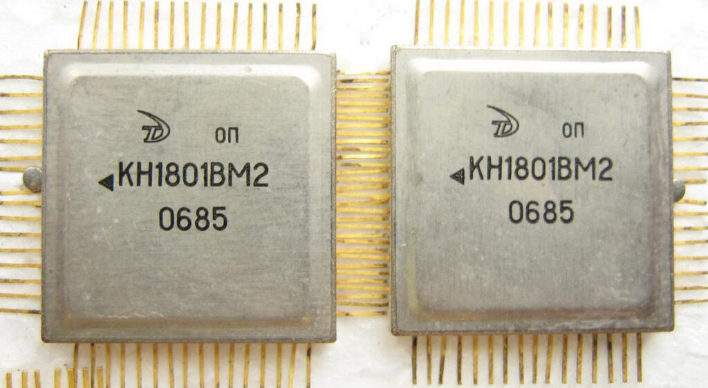
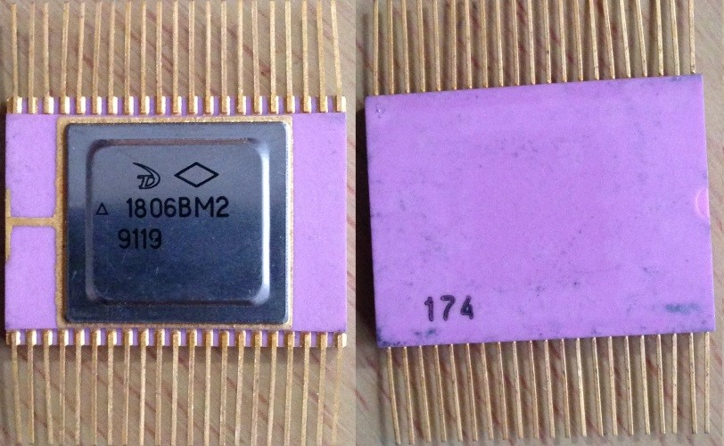
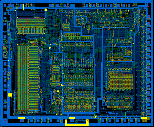
 1801VM2 die |
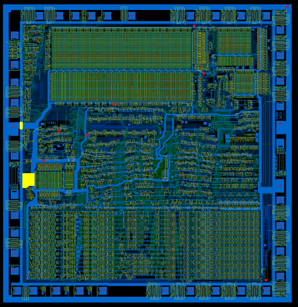
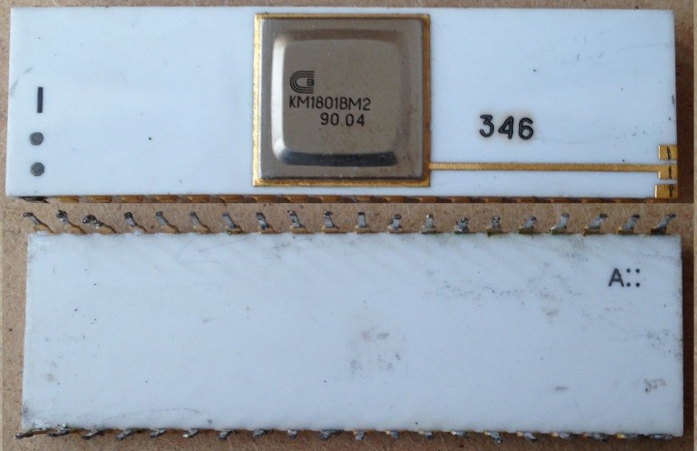
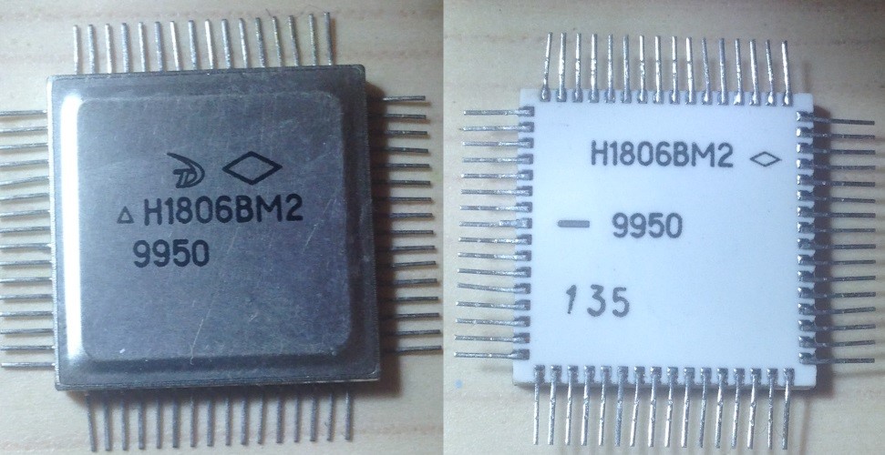
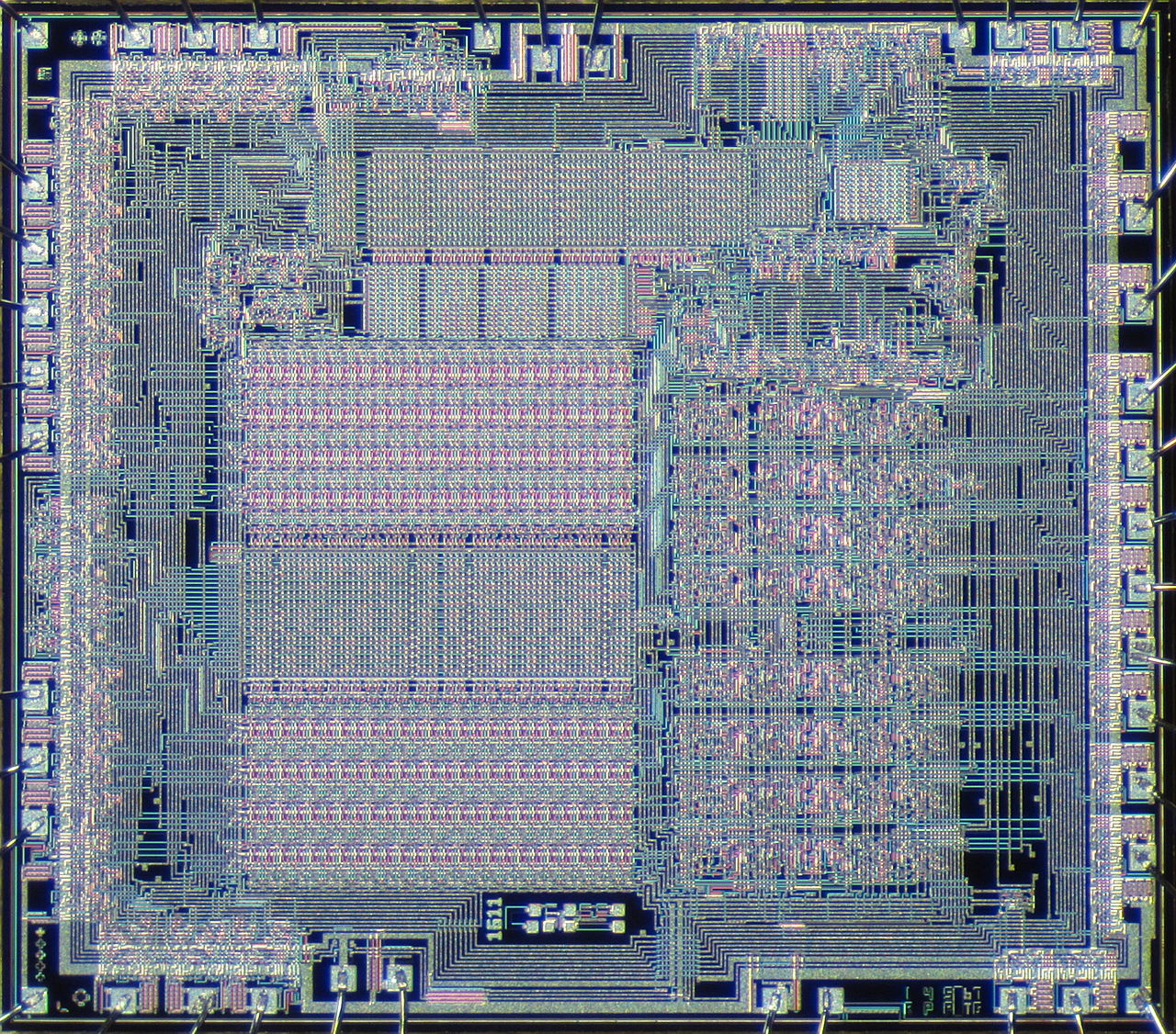
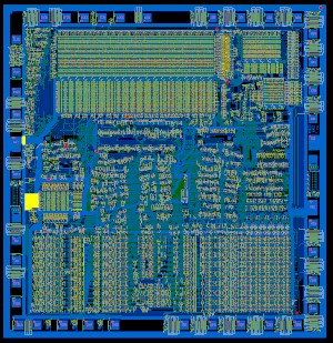
 1801VM3 Die |
1801VM3 Specifications
- Number of processor Instruction: 72 Fixed Point and 46 Floating Point (with 1801VM4 FPU)
- Address Space: 4MB
- General Purpose Registers: 8
- Manufacturing process: 4 micron N-channel silicon gate MOS technology (later migrated to 3 micron)
- Die size 6.65 × 8 mm
- Transistor count: 28,900 active transistors, 200,000 integral elements
- Clock rate: 4MHz (1801VM3V) 5MHz (1801VM3B) 6MHz (1801VM3A, upgraded to 8 in 1991)
- Performance: For register based operations (like addition) up to 1,500,000 instruction/s (1.5 MIPS)
- IRQ Lines: 4
- Supply voltage + 4.75V-5.52V
- Power consumption: 1.7-2 W
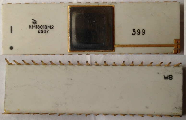
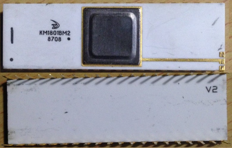
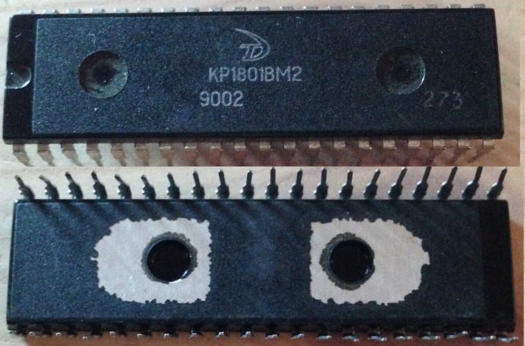
- Packages: CDIP64 (KM1801VM3) LQFP64 (KA1801VM3) CQFP64 (KN1801VM3/N1801VM3)
Like the VM2 before it the speeds were denoted by a series of dots on the package (or lack thereof)
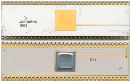
KM1801VM3A – 6MHz (no extra dot) CDIP64 package from 9008
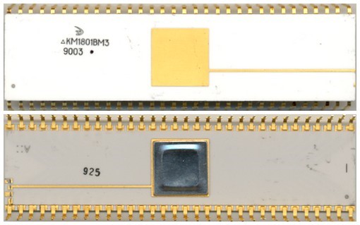
KM1801VM3B – 5MHz (one extra dot) CDIP64 package from 9003
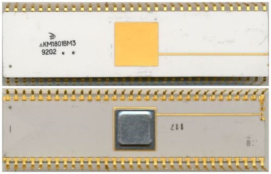
KM1801VM3V – 4MHz (two extra dots) CDIP64 package from 9202
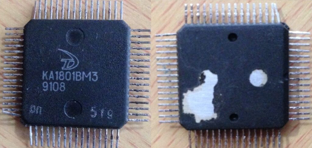
KA1801VM3 – 8MHz (no extra dot – post 1991) PQFP64 package from 9108
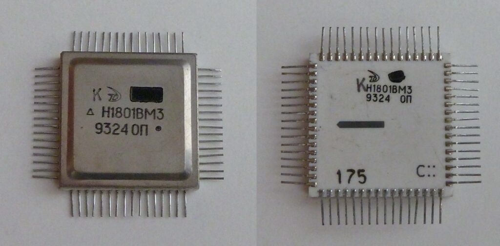
N1801VM3 – 8MHz (no extra dot – post 1991) CQFP64 package from 9324 – Remarked from a military part (rhombus marking marked over)
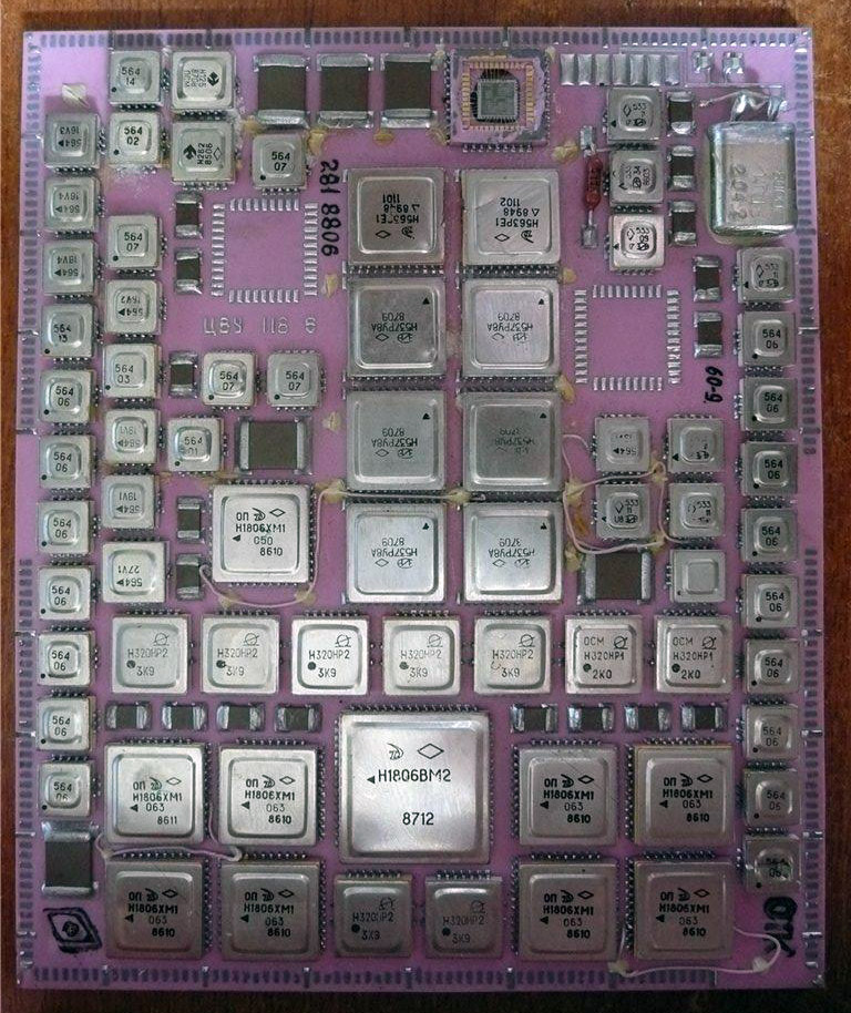
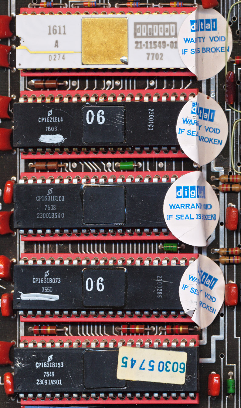
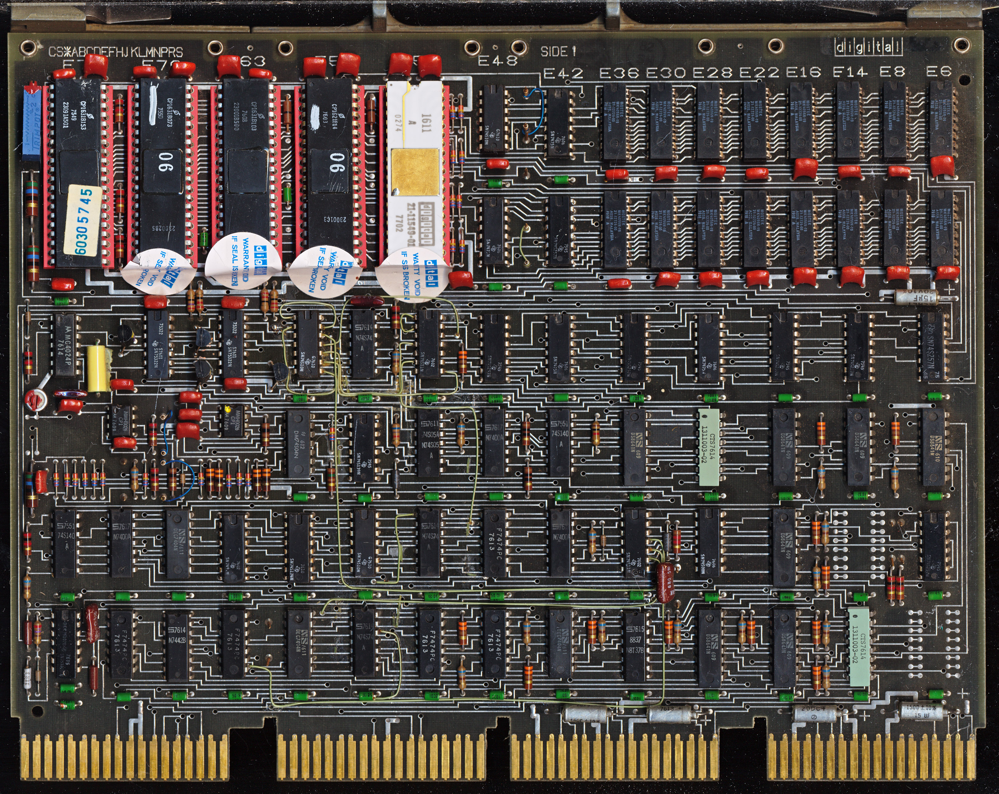
The KM1801VM3 appeared as part of the DVK line of computers, starting with the DVK-3M model (PCB ”Electronics МС 1201.03” and “Electronics МС 1201.04”). Using the same ISA (Instruction Set Architecture) allowed DVK (and others) to rapidly update their computer line when new processors were available, and allow for a wider software base. This is very much like the original IBM PC using the x86 architecture. The transition from 8086 to 80286 was relatively easy to design, and nearly seamless for the end user.
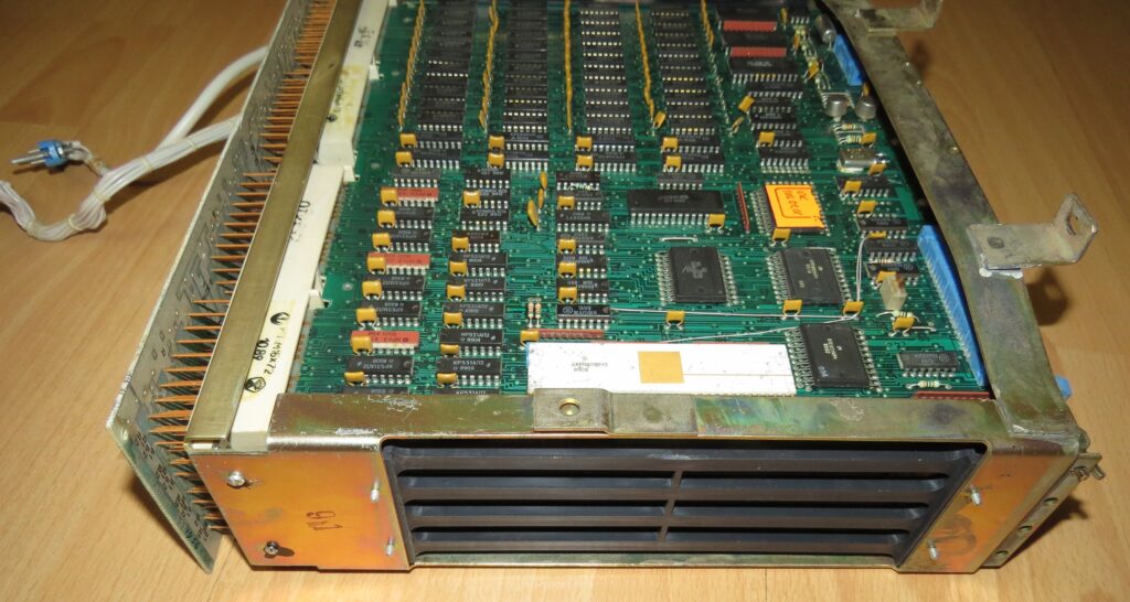
DVK PCB Electronics МС 1201.03 board on the top.
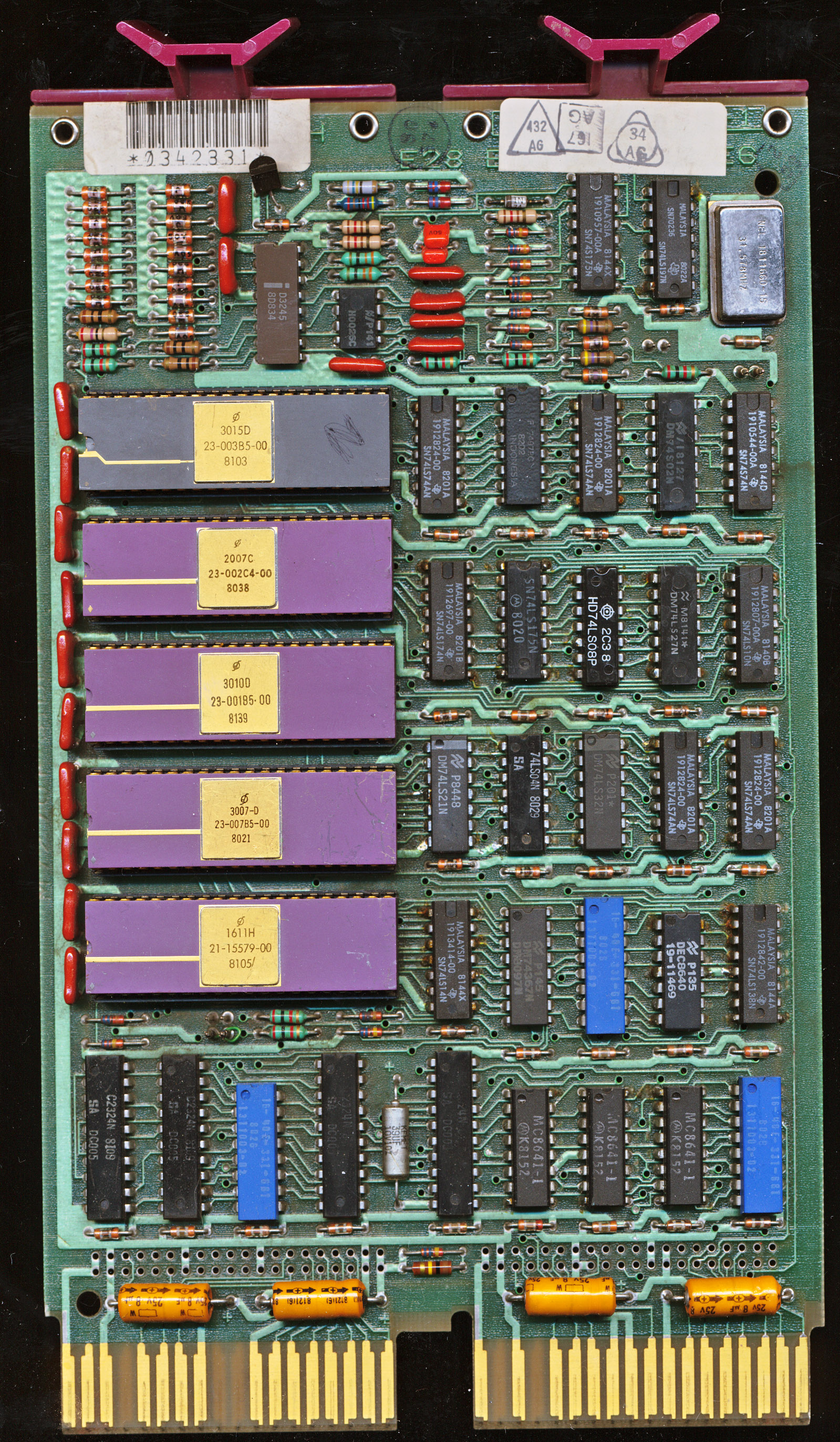
Many devices built on the basis of the 1801 series CPU contain other microcircuits of the same series (support circuits).
In addition to microprocessors, this series includes:
– ULA 1801VP1-xxx
– masked ROM 1801REх-xxx
– EEPROM 1801RR1
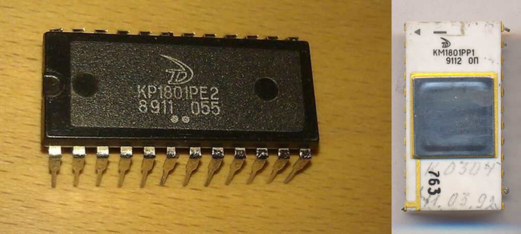
ULA and EEPROM
The 1801VP1-xxx is a ULA- (Uncommitted Logic Arrays). It’s made using a 3 micron N-channel silicon gate MOS technology with one metal layer. First, base silicon wafers are made that contain transistors. These are doped regions of silicon and a separate oxide-insulated layer of polysilicon gates. Then all this is covered with an oxide layer. Base wafers are ready.
In this form, the wafers can be stored for a long time or transferred to another fab. All 1801VP1-xxx chips, regardless of number, have the same structure and arrangement of transistors. And they are made on the same base wafers.
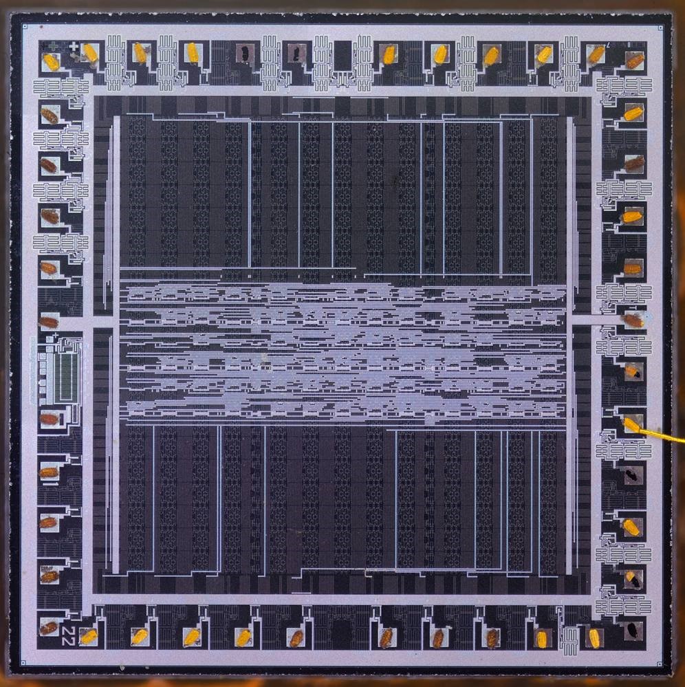
KR1801VP1-22 die
Differences between the chips appear only at the last stage of manufacturing. In the upper oxide layer, the die is etched by photolithography to access the required transistors. And then form a metallic pattern from aluminum. This pattern defines the electrical circuit. The number in the marking identifies the purpose of the chip. For example, 1801VP1-033 is an external device controller. This is similar to how a MaskROM is made but instead of only memory elements, it contains logic elements allowing for a custom IC to be made (like a mask programmable PAL/GAL)
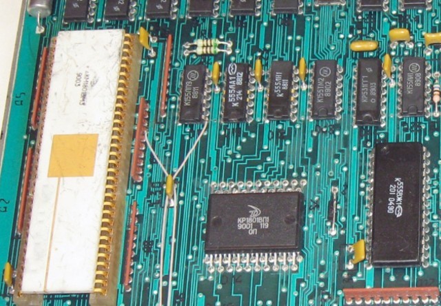
KR1801VP1-119
The 1801VP1-119 is a companion chip for 1801VM3. It can be said to be the “north bridge“.
The 1801VP1-119 performs the following functions:
-forms control signals for DRAM;
-forms control signals for system SRAM;
-generates signals to select system ROM;
-generates control signals for detection and correction of memory errors (EDC) using Hamming code (555VGH1). Error correction circuits reduced performance by 10-15%. Therefore in some computers, there were jumpers to enable/disable the EDC
-buffer data register control;
-generate other signals
This was the beginning of what would be come chipsets, replacing loads of TTL with custom circuits. The exact same evolution was occurring in the west with the PC environment, until nearly all the support circuits were integrated into just a couple large ASICs. Its interesting to see the development paths of the Soviet computers and the West. While they were entirely different instruction sets, they evolved in very much the same way. East or West, LSI-11 or x86, at the end of the day, a computer is a computer and will evolve in similar fashion.
Posted in:
CPU of the Day