January 2nd, 2020 ~ by admin

Chips in Space: Making MILSTAR
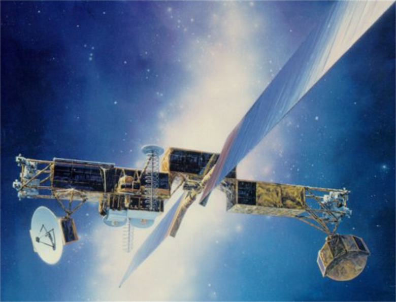
Milstar Satellite

Back in the late 1970’s having a survivable space based strategic communications network became a priority for the US Military.  Several ideas were proposed, with many lofty goals for capabilities that at the time were not technologically feasible.  By 1983 the program had been narrowed to a highly survivable network of 10 satellites that could provide LDR (Low Data Rate) strategic communications in a wartime environment.  The program became known as MILSTAR (Military, Strategic, Tactical and Relay) and in 1983 President Reagan declared it a National Priority, meaning it would enjoy a fair amount of freedom in funding, lots and lots of funding.  RCA Astro Electronics was the prime contractor for the Milstar program, but during the development process was sold to GE Aerospace, then Martin Marietta, which became Lockheed Martin before the 3rd satellite was launched.  The first satellite was suppose to be ready for launch in 1987, but changing requirements delayed that by 7 years.

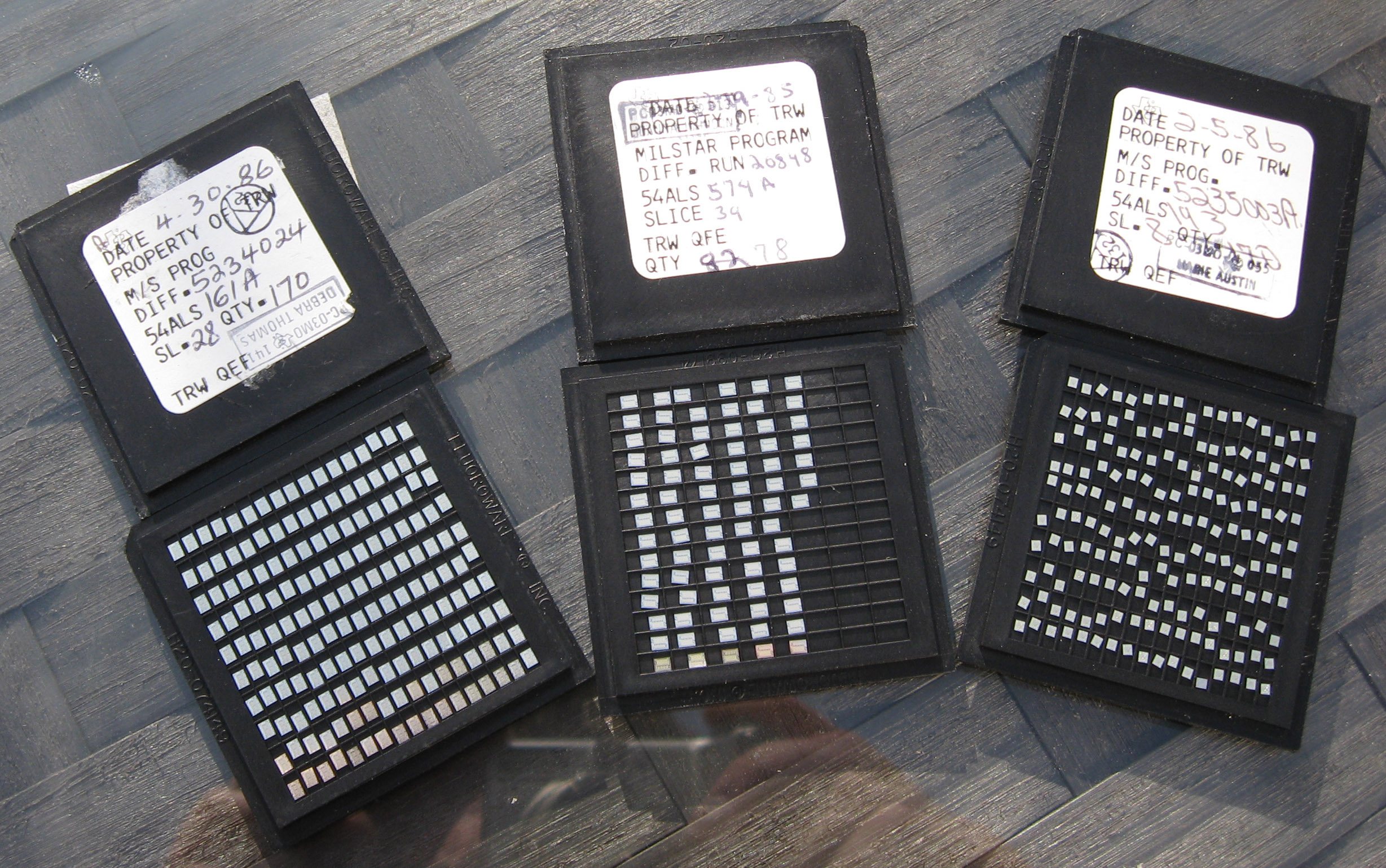
Milstar Program 5400 series TTL dies

The first satellite was delivered in 1993 and launched in February of 1994.  A second was launched in 1995 and these became Milstar-1. A third launch failed, which would have carried a hybrid satellite that added a Medium Data Rate (MDR system).  Three Block II satellites were launched in 2001-2003 which included the MDR system, bringing the constellation up to 5.  This provided 24/7 coverage between the 65 degree N/S latitudes, leaving the poles uncovered.
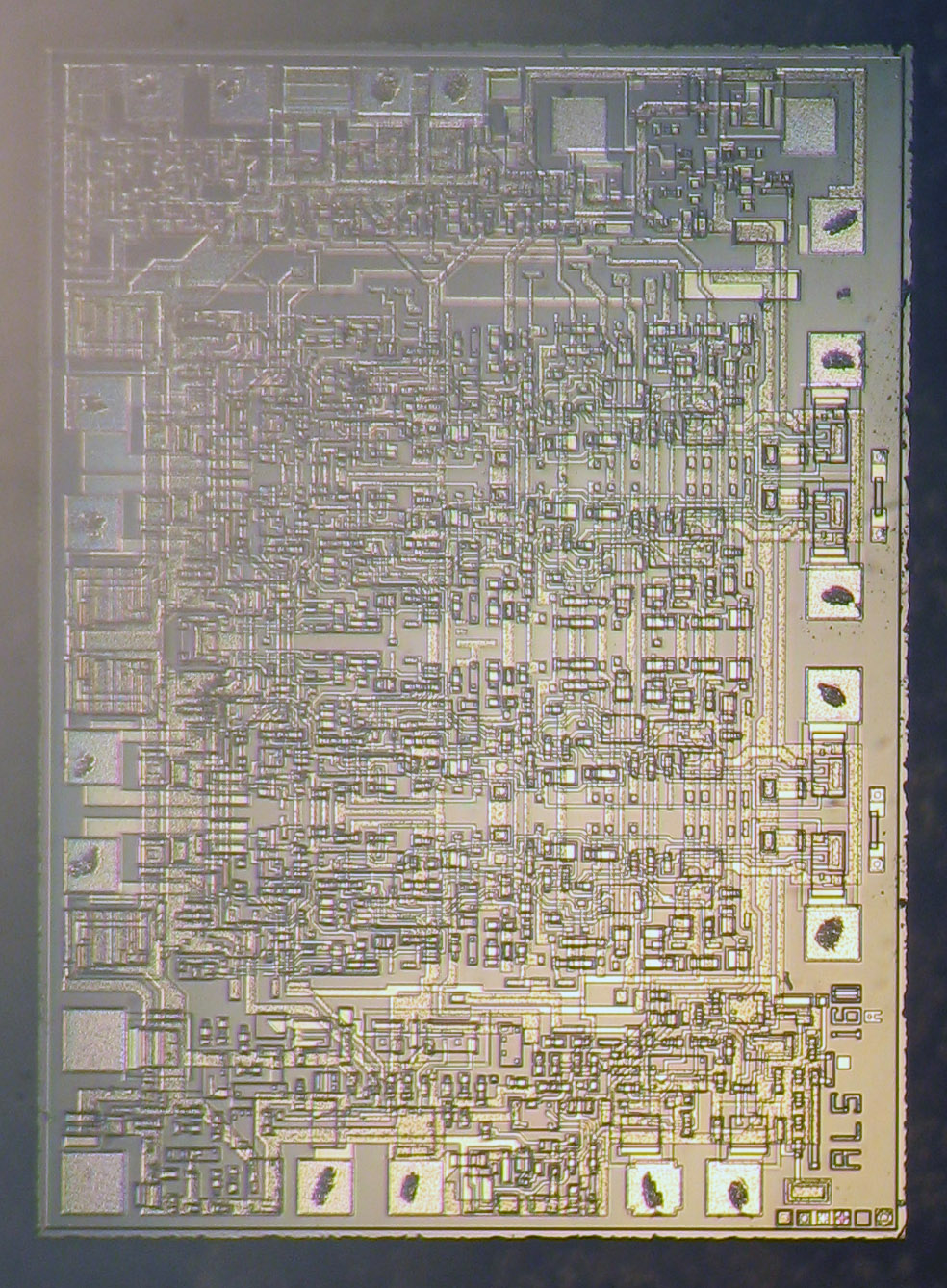
TI 54ALS161A

The LDR payload was subcontracted to TRW (which became Northrup Grumman) and consisted of 192 channels capable of data rates of a blazing 75 – 2400 baud.  These were designed for sending tasking orders to various strategic Air Force assets, nothing high bandwidth, even so many such orders could take several minutes to send.  Each satellite also had two 60GHz cross links, used to communicate with the other Milstar sats in the constellation.  The LDR (and later MDR) payloads were frequency hopping spread spectrum radio system with jam resistant technology.  The later MDR system was able to detect and effectively null jamming attempts.

The LDR system was built out of 630 LSI circuits, most of which were contained in hybrid multi layer MCM packages.  These LSIs were a mix of custom designs by TRW and off the shelf TTL parts.  Most of the TTL parts were sourced from TI and were ALS family devices (Advanced Low Power Schottky), the fastest/lowest power available.  TI began supplying such TTL (as bare dies for integration into MCMs) in the mid-1980’s.  These dies had to be of the highest quality, and traceable to the exact slice of the

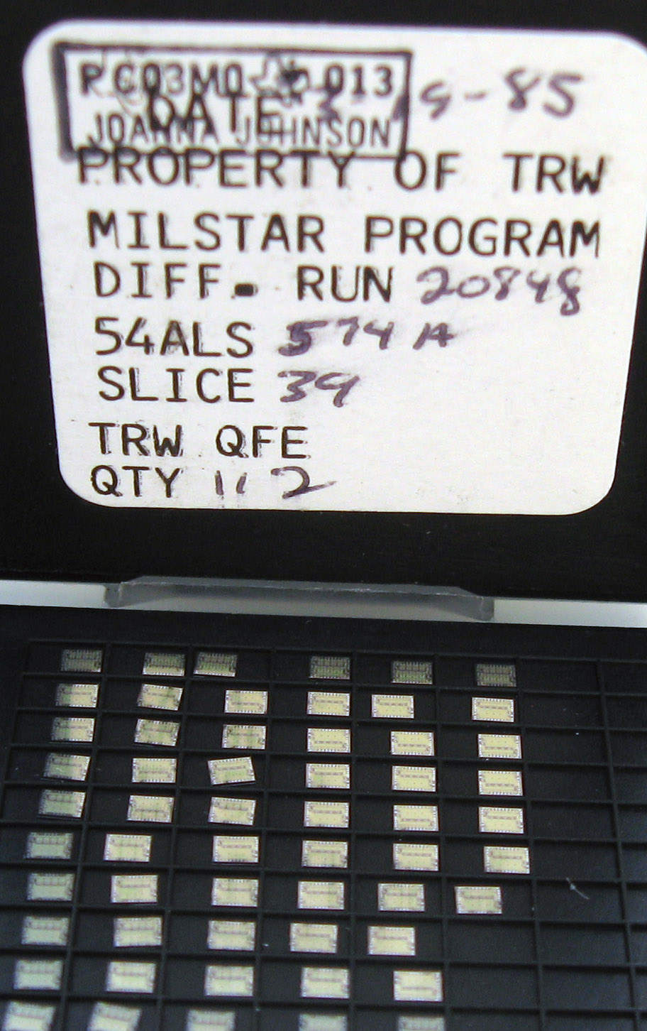
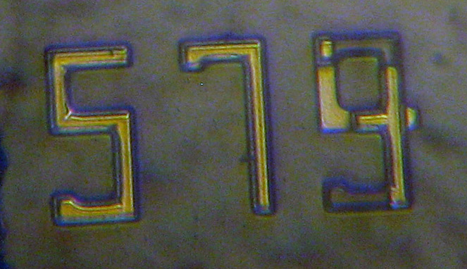
Traceability Markings

exact wafer they came from. They were supplied in trays, marked with the date, diffusion run (a serial number for the process and wafer that made them) and the slice of that wafer, then stamped with the name/ID of the TI quality control person who verified them.

These TTL circuits are relatively simple the ones pictures are:
54ALS574A Octal D Edge Triggered Flip flop (used as a buffer usually)
54ALS193 Synchronous 4-Bit Up/Down Binary Counters With Dual Clock
54ALS161A Asynchronous 4-Bit Binary Counters
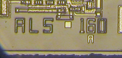
ALS160-161

Looking at the dies of these small TTL circuits is quite interesting.  The 54ALS161A marking on the die appears to be on top of the a ‘160A marking.  TI didn’t make a mistake here, its just that the the 160 and 161 are essentially the same device.  The 161 is a binary counter, while the 160 was configured as a decade counter.  This only required one mask layer change to make it either one.

ALS573 and ALS574 die

Similarly with the 54ALS574, which shares a die with the more basic ‘573 D type transparent Latch.  This was pretty common with TTL (if you look at a list of the different 7400 series TTL you will notice many are very similar with but a minor change between two chips).  It is of course the same with CPUs, with one die being able to be used for multiple core counts, PCI0E lanes, cache sizes etc.

Together with others they perform all the function of a high reliability communications systems, so failure was not an option.  TI supplied thousands upon thousands of dies for characterization and testing.  The satellites were designed for a 10 year lifetime (it was hoped by them

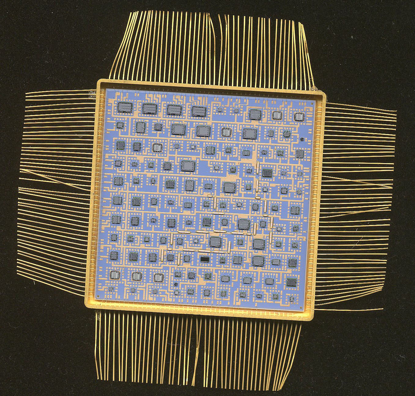
Milstar Hybrid MCM Command Decoder (picture courtesy of The Smithsonian)

something better would be ready, no doubt creating another nice contract, but alas, as many things are, a follow on didn’t come along until just recently (the AEHF satellites).  This left the Milstar constellation to perform a critical role well past its design life, which it did and continues to do.  Even the original Milstar 1 satellite, launched in 1994 with 54ALS series TTL from the 1980s is still working, 25 years later, a testament to TRW and RCA Astro’s design.  Perhaps the only thing that will limit them will be the available fuel for their on-orbit Attitude Control Systems.

While not necessarily a CPU in itself these little dies worked together to get the job down.  I never could find any of the actual design, but it wouldn’t surprise me if the satellites ran AMD 2901 based systems, common at the time or a custom design based on ‘181 series 4-bit ALUs.  finding bare dies is always interesting, to be able to see into whats inside a computer chip, but to find ones that were made for a very specific purpose is even more interesting.  The Milstar Program cost around $22 Billion over its life time, so one must wonder how much each of these dies cost TRW, or the US Taxpayer?

Tags:
, ,

Posted in:
CPU of the Day

July 16th, 2015 ~ by admin

TI SN74LS481: A Better Bit-Slicer

TI SN74LS481J -1980 - 8 MHZ 4-bit Slice

TI SN74LS481J -1980 – 8 MHZ 4-bit Slice

The 1970’s was a rush to design new and innovative processors, faster, more features, and more bits.  Most of the processors were new designs, a few were single chip implementations of older mainframes (such as the TMS9900 and the Intersil 6100.  At the same time there was a competition of 4-bit processors.  Somewhat remarkable in 1976 considering 16-bit designs were now being released.  The most famous was of course the AMD AM2901, which undoubtable won the battle.  There were others, the MMI 6701 (a company which AMD would go on to merge with).  Motorola had the MC10800, made in ECL and Intel made the ill-fated (probably since it was only 2-bits) Intel 3002 Processor.  TI made the SBP0400 in I2L that enjoyed some success, but that apparently wasn’t enough.  In 1976, the same year as the SBP0400, the 6701 and the AMD AM2901, TI released the SN74S481.  This was a Schottky TTL 4-bit slice processor (and the SN74S482 sequencer for it).  It was a bit different than its competition.

Read More »

Posted in:
CPU of the Day

February 5th, 2015 ~ by admin

TI TMS9900/SBP9900: Accidental Success

TI TMS9900JL - 1978

TI TMS9900JL – 1978

In June 1976 TI released the TMS9900 16-bit processor.  This was one of the very first 16-bit single chip processor designs, though it took a while to catch on.  This is no fault of its own, but rather TI’s failure to market it as such.  The 9900 is a single chip implementation of the TI 990 series mini-computers.  It was meant to be a low end product and thus was not particularly well supported by TI, who did not want to cut into the higher margins of their mini-computer line.    By the late 1970’s TI began to see the possibilities of the 9900 as a general purpose processor and began supporting it with development systems, support chips, and better documentation.  If TI had marketed and supported the 9900 from its release the microprocessor market very much may have turned out a bit different.  A large portion of Intel’s success (with the 808x) was not due to a good design, but rather good support and availability.

The original TMS9900 was a 3100 gate (approx 8000 transistors) NMOS design running at up to 3MHz.  It required a 4-phase clock and 3 power supplies (5V, 12V, -5V).  It had a very orthogonal instruction set that was very memory focused, making it rather easy to program.  General purpose registers were stored off chip, with only a PC, Workspace Register (which pointed to wherever the general registers would be) and a Status Register on chip.  This made context switching fairly quick and easy.  A context switch required saving only 2-3 registers. The 9900 was packaged in a, then uncommon, and expensive, 64 pin DIP.  This allowed the full 15-bits of address and 16-bits of data bus to be available.

TI had a trick up their sleeve for the 9900 line…

Read More »

Posted in:
CPU of the Day

August 30th, 2014 ~ by admin

Improve Technologies Make-it 486 – 286 Upgrade

Cx486SLC/e-33MP Based Improve Technologies Make-It 386 for a 286

Cx486SLC/e-33MP Based Improve Technologies Make-It 386 for a 286

Improve Technologies (IT) was a company that existed from 1991-1997.  They were one of the many (to include Cyrix, Evergreen, PNY, Gainbery, etc) that made processors for upgrading 286, 386 and 486 computers.  Processor upgrades are no longer commonplace, becoming nearly non-existent (except for such things as 771 to 775 adapters).  Today computer hardware has become so inexpensive that upgrading more often just consists of purchasing a whole new computer, or at least new motherboard, RAM, and CPU, all at a price of a few hundred dollars.

In the early to mid-90;s however, a computer system cost 2-$3000, so replacing it every few years was not financially viable for many people.  Thus processor upgrades, they were designed to replace a CPU with the next generation CPU (with some limitations) at a price of a few hundred dollars.

In 1976 TranEra was founded in Utah. TransEra is an engineering solutions company, they are built on seeing a technological problem, and engineering a solution, whatever that may be.  They began by making add-on for Tektronix test gear and HP-IB interface equipment.  In 1988 they released HTBasic, a BASIC programming language (based on HP’s Rocky Mountain BASIC) for PC’s.  This is what TransEra became perhaps best known for, as they continue to develop and sell HTBasic.  It was TransEra who developed the Improve Technologies line of upgrades.  They saw a problem, and engineered a solution.

Read More »

Tags:
,

Posted in:
CPU of the Day

January 18th, 2013 ~ by admin

CPU of the Day: Cypress CY7C601 25MHz SPARC

Cypress CY7C601-25GC

Cypress CY7C601-25GC – First package with heatspreader – Omitted on later versions

In Mid-1987 Sun Microsystems (now owned by Oracle) released the SPARC (Scalable Processor ARChitecture)  processor architecture to be used in their computers (replacing the 68k based systems they had previously used).  The SPARC was designed from the outset to be an open architecture, allowing manufactures to license and built processors that implemented it using whatever technology they wished.  The goal of this was to 1) build a large SPARC ecosystem and 2) keep prices in check by fostering competition among manufacturers.  The SPARC is still used today by Oracle, Fujitsu, the European Space Agency and others, owing largely to its design as an open architecture from the very beginning.

The first version was made by Fujitsu on a 20,000 gate array at 1.2 micron and ran at 16.6MHz.  In July 1988 Cypress  (later to be spun off as Ross and make the famous HyperSPARC line) announced the CY7C601.  This was the fastest implementation of the SPARC at the time.  It was made on 0.8u CMOS process and contained 165,000 transistors, dissipating around 3.3Watts.  As was typical of many processor designs of the time, it was an integer only processor, requiring a separate chip (the CY7C602) for floating point work.  In September of 1988, Cypress cross licensed the ‘601 to Texas Intruments in exchange for rights to the 8847 floating point processor.  This was mainly to appease one of Cypress main customers who demanded that a second source for the ‘601 chips be available, a demand more common in the 1970s then in 1988 but Cypress obliged.  Cyrpress also gained the rights to make the next generation SPARC processor that TI was developing.  TI would go on to make many SPARC processors, and continued to be the primary fab for Sun up through the SPARC T2 Plus in 2008.  Oracle now used TSMC to fab the T3 and T4 SPARC processors.

Tags:
, , ,

Posted in:
CPU of the Day

February 14th, 2011 ~ by admin

Processor News Round-up: More cores in more places

The last week has been filled with new processor announcements, mainly for phones, but cameras as well. (yes they run some powerful processors now too).

TI is barely shipping products with its dual-core OMAP 4 applications processor and has already announced its successor, the OMAP 5.  The OMAP 5 will be a 2GHz dual core ARM Cortex-A15 (the next ARM generation after the A9). It also includes a pair of ARM Cortex-M4 processor.  the Cortex-M4 is a 150-300MHz microcontroller oriented processor.  This will allow the OMAP 5 to run basic background tasks on the slower (lower power) cores while reserving the high power cores for tasks that actually need them, increasing battery life.

Broadcom continues its drive to enter the smart phone business with the BCM28150, a 1.1GHz dual core ARM Cortex-A9 compatible with Google Android.  In December they released the BCM2157, a 500MHz dual core ARM11 processor for low-end smart phones

Samsung decided to rename the Orion processor (announced back in November) to the Exynos 4210.  A bit of a mouthful compared to Orion.

Fujitsu MB91696AM

Qualcomm showed off the  APQ8060 in HP’s new TouchPad.  This is a dual core version  Snapdragon processor we have become very familiar with. Qualcomm has an architecture license from ARM so they are free to design their own cores without having to stick to ARMs own implementations (such as Cortex-A9 etc).  This gives Qualcomm more flexibility to design in features they need, and tweak design more best efficiency.

Smart phones aren’t the only ones getting new processors.  Digital cameras now require immense amount of processing power (especially to handle 1080p video recording.  Fujitsu (yah, they still make a lot of processors) announced the Milbeaut MB91696AM.  This is a dual core ARM processor with many other DSP functions capable of handling 14Mpixel shooting at 8fps, as well as full HD video.

May 16th, 2009 ~ by admin

TI Grabs Luminary by the ARM

TI has purchased Luminary Micro for an undisclosed amount of money.  TI, one of the larger producers of embedded processors, and applications processors for mobile phones add significantly to their portfolio by adding Luminary, maker of ARM Cortex based microcontrollers.  Most of TI’s line of processor are now ARM based. They do of course also make MCS-51 products as well as their VERY widely used DSP series (such as the TMS320 series).

Source: EE Times

January 13th, 2009 ~ by admin

Dual core CPU…For $1?

When you think of multi-core CPU’s what comes to mind? Intel? AMD? Perhaps Nvidia, but certainly not TI.

Alas though, the embedded CPU/MCU market is by far the largest user of multicore CPU’s.  Many systems controllers have an ARM main core, and then a MCS-51 core for IO stuff, or another ARM core.  The iPhone has no less then 3 ARM cores in it.

TI just released the MSP430FE42X2, in large quantities its a mere $1 US. It includes 2 complete MSP430 cores, along with an LCD driver, and 32K of Flash.  Where will you find it? Its marketed as a complete power meter solution, only other component needed to measure your houses power draw is a voltage regulator.


MSP430 Power Meter

MSP430 Power Meter

The future of embedded computing IS multi-core controllers/ASICs

Source:  TI (Texas Instruments)

Tags:
, ,

Posted in:
Processor News

January 12th, 2009 ~ by admin

Processor Find of the Day

Today I got a not so old (2006) Infocus IN24 projector.  It had bit the dust due to corrosion  from the warm salty air in Maui.

What did I find inside? besides some amazingly cool optics, and power components, there was a large TI DLP Processor, specifically the DDP2000, a rather large BGA chip, that integrates most of the projectors functions as well as a DSP core, and a ARM 946 CPU core. running at 120MHz, good enough for 800×600 resolution.

Processor is the one marked DLP, bare die is a SRAM, far right is the DLP mirror, imaging chip (just layed on the board for your viewing)

projector

Ti DLP ARM CPU and Sensor

[ad]

Tags:
, ,

Posted in:
CPU of the Day