
The Soviet 1801VM2 LSI-11 Processor
The Soviet-made 1801VM2 CPU (a binary-compatible implementation of the PDP11 instruction set and QBUS interface) was developed in 1982. The 1801VM2 is a further development of the earlier 1801VM1 doubling the original 5MHz clock speed. From a constructive standpoint this CPU is a completely independent development.
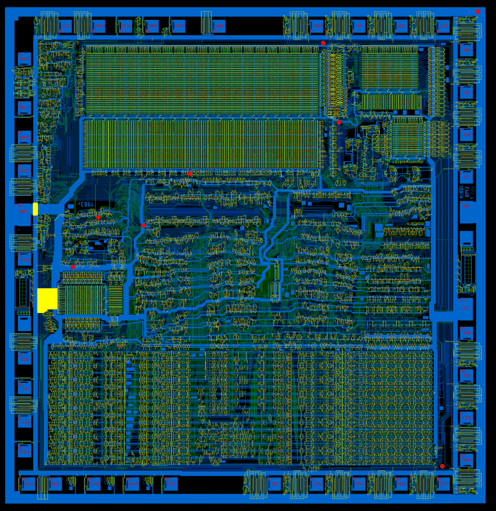
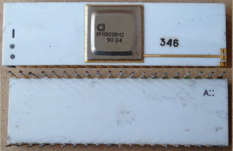
1801VM2 die – 1983 dated
1801VM2 Specifications
- Number of processor Instruction: 72
- Manufacturing process: 4 micron N-channel silicon gate MOS technology
- Die size 5.3 × 5.35 mm
- Transistor count: 18,500 active transistors, 120,000 integral elements
- Clock rate: Up to 10 MHz
- Performance: For register based operations (like addition) up to 1,000,000 instruction/s (1 MIPS) – for operations like multiplication, up to 100,000 instructions/s
- Supply voltage + 5V
- Power consumption: up to 1.7 W
- The case is 40-lead, ceramic DIP (KM1801VM2) or plastic DIP (KR1801VM2). (a surface mount version was also made)
To increase noise immunity in comparison with 1801VM1, additional ground contacts were made for the address / data bus.
The 1801VM2 was manufactured at two factories: Angstrem and Solnechnogorsk Electromechanical Plant (SEMZ). As was typical of the time speed grading was done by adding extra marking to the chips post-testing. Its very easy to miss these, if a chip was tested at 10MHz and passed it received no extra marking and was considered an 1801VM’A.’ If the device failed at 10MHz but ran at 8MHz a small dot was added to the package (and was considered a grade ‘B’ device). This dot was not to be confused with the dot for the pin one marker, though often placed…next to it.
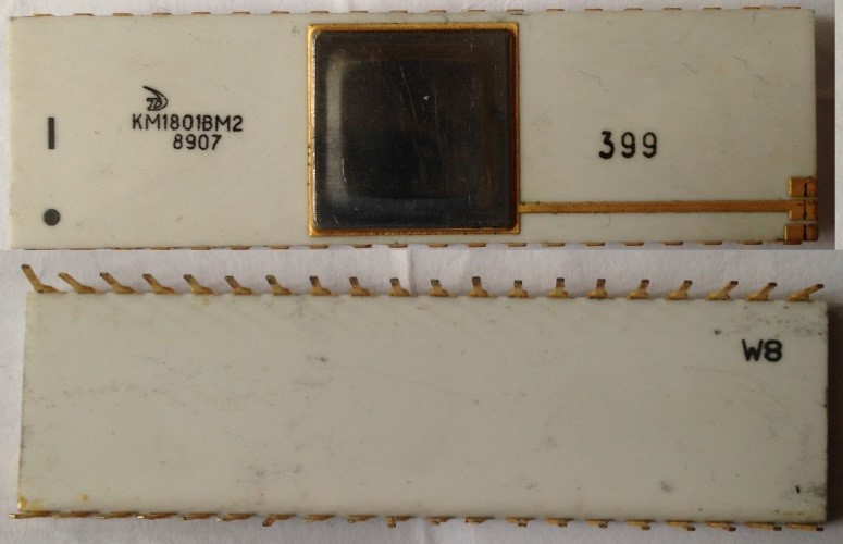
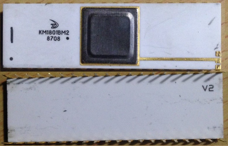
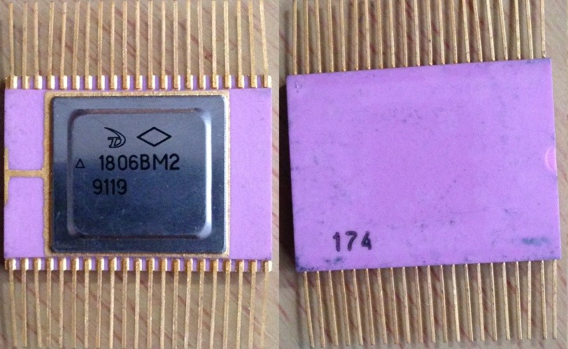
Ceramic DIP 1801VM2A Angstrem – 1989 No extra dot
Ceramic DIP 1801VM2B Angstrem – 1987 – Note the extra dot in this case by the date code
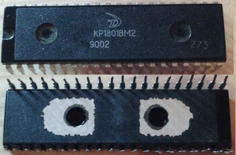
Plastic DIP 1801VM2A Angstrem – 1990
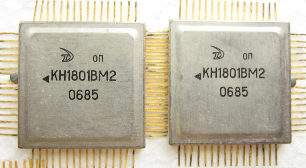
KN1801VM2- Angstrem 1985 CQFP Surface mount version (image Baator)
Ceramic DIP 1801VM2 Solnechnogorsk Electromechanical Plant – 1990 – Extra dot by pin 1 marker
In comparison with 1801VM1, expanded arithmetic instructions (MUL, DIV, ASH, ASHC – part of a the set of PDP-11 EIS), and also operations from the floating point instruction set (FIS) were added. The FIS instructions (FADD, FSUB, FMUL, FDIV) are realized through subroutines – when performing these instructions there is a special type of interrupt and the program handler in memory (“shadow” system ROM K1801RE2) of the console mode is executed, a ‘firmware’ style of FIS implementation, as its not truly hardware (the ROMs break down the FIS instructions into something the 1801VM2 can execute)
During the design of the microprocessor, a microcode error was made, leading to a malfunction of the processor when reading with addressing method 17 ( MOV (PC), R0).
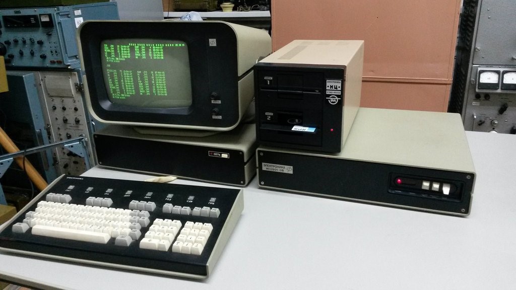
DVK-1 Computer
The 1801VM2 was the heart of a number models of DVK computer. DVK was developed at the Research Institute of Precision Technology , Zelenograd (just outside of Moscow). The first model DVK-1 was developed in 1981, and released in 1983. Architecturally DVK copies mini-computers from DEC PDC-11 and PDP-11. By 1990, 200,000 DVK computers of the nine different models were produced.
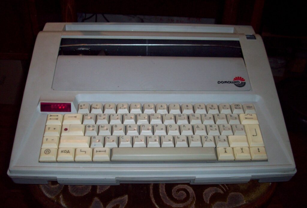
Romashka Word Processor
Use of the processor continued well into the 1990’s. The “Romashka” belonged to the latest generation of electronic typewriters, which in their functionality were close to computer text editors. This typewriter made it possible to automatically format text (set alignment, change the spacing between characters and between lines, use bold and underlined fonts, etc.) and had an electronic memory of at least one page (3800 bytes). In the West these half typewriter half computer were called Word Processors, and were quite popular through the 1980’s. The machine’s control unit was a microcomputer based on the KM1801VM2 processor.
“Romashka” was produced by the Kursk PO “Schetmash” in the first half of the 1990s.
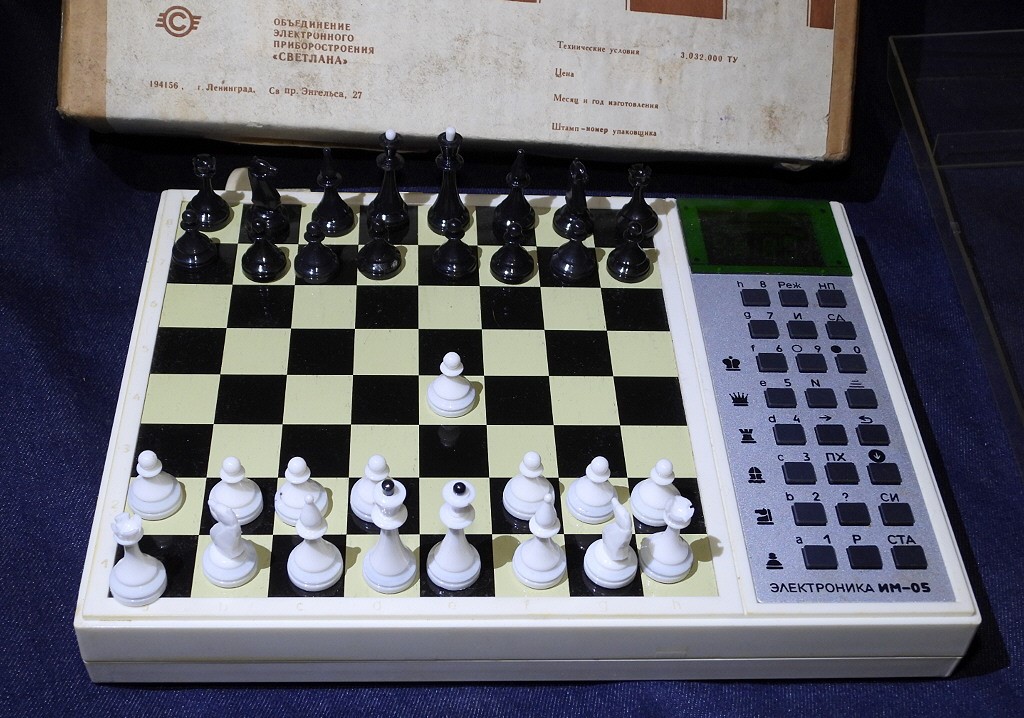
“Electronics IM-05 “- Soviet chess computer, contains 1801VM2 inside. It was a continuation of the line of chess computers “Electronics”. Produced by the Svetlana Association, Leningrad.
In 1984, the military-grade microprocessor 1806VM2 was released.
This microprocessor functionally corresponds to the 1801VM2, but is made using CMOS technology.
- Clock rate: up to 5 MHz
- Number of Instructions: 77
- Contains 134,636 integral elements
- Power consumption: up to 0.025W
The 1806VM2 developers fixed the microcode bug present in 1801VM2 (much to the relief, or annoyance of programmers). The 1806VM2 was supplied in a 42-lead dual in-line ceramic package with flat leads, N1806VM2 in a 64-lead CQFP. The rhombus marking on the chips denotes a military-grade device.
1806VM2 – Angstrem 1991 in the nice pink flat pack
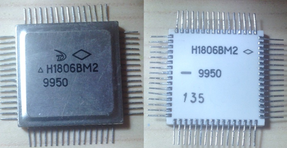
N1806VM2 – Angstrem 1999 in a Ceramic quad flat pack
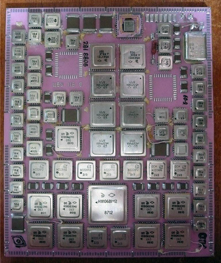
CQFP N1806BM2 on a ceramic substrate forming a military Single Board Computer – circa 1987 (image Baator)
These 1806VM2 are still being made by Angstrem, if you need to build a PDP-11 computer to run Tetris on, or repair a Buran shuttle you may have laying around.
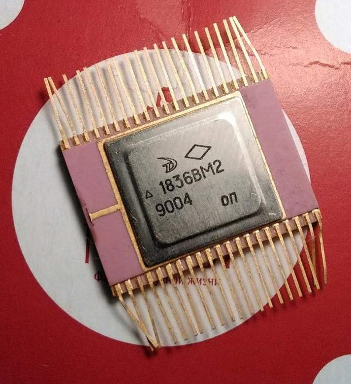
In 1990, a radiation-hardened microprocessor was introduced, compatible with the 1806VM2, known as the 1836VM2/N1836VM2. Just like in other countries, existing code base and known reliability are more of a driver of what the military/industry uses than having the latest and greatest. There are still MIL-STD-1750A processors being made and used, rad-hard 8051s and 80186s, and Soviet PDP-11 processors right there with them.
Photos of microprocessors from the collection of Perfiliev Andrey (Andreycpu).
Article written originally by Contributing Author Vladimir Yakovlev (edited by cpushack)
November 4th, 2021 at 7:39 pm
That die image looks too precise to be a photograph. Is it actually a rendering? Could you say where you got it?
November 4th, 2021 at 10:12 pm
Its basically a version made from a die photo, showing the layout/routing/pads from a reverse engineering project.
https://github.com/1801BM1/cpu11/tree/master/vm2
November 5th, 2021 at 1:45 am
I flew to a conference in Szeged, Hungary in 1987, paid for out of an AFNOR “Star Wars” grant.
Soviets were very interested in semiconductor defects, and how to make their devices work despite them, because their wafers were not good. That probably accounts for much of the delay between Soviet and western chip developments; big features make for better defect tolerance.
November 5th, 2021 at 9:24 am
Those are astonishingly low power consumption numbers, even by old-school 8-bit micro standards.
November 7th, 2021 at 12:09 pm
You transliterate ВМ into VM, then the “Н” needs to be changed into N everywhere as well.
November 17th, 2021 at 7:35 pm
Very true, just fixed it, Thanks!
August 13th, 2022 at 7:44 am
“…a microcode error was made, leading to a malfunction of the processor when reading with addressing method 17 ( MOV (PC), R0).”
Source addressing method 27 (MOV (PC)+, R0 or MOV #imm,R0) was important to PDP-11 programmers, but I cannot see any use for method 17. (It accesses the opcode of the next instruction.) How was that microcode error a problem?