August 2nd, 2021 ~ by admin

The 6502 Travels the World: The Story of the Indian SCL6502

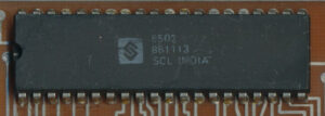
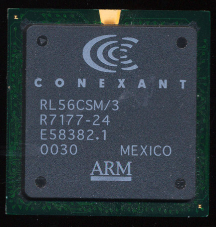
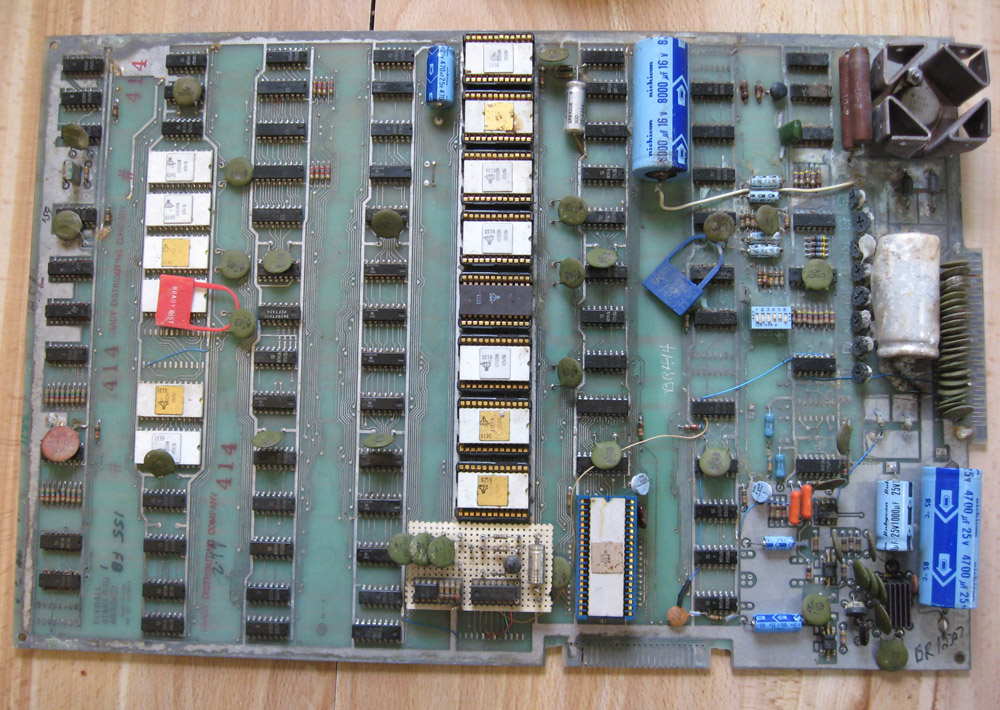
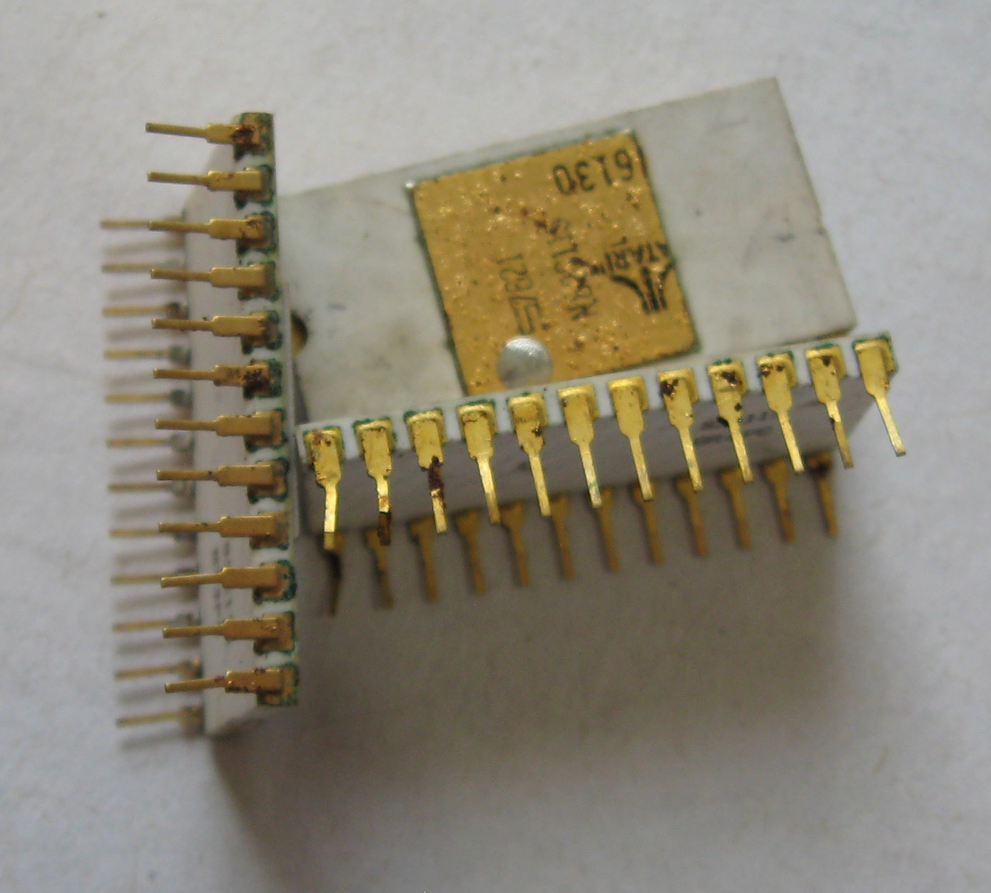
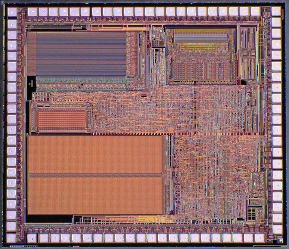
Semiconductor Complex LTD SCL6502 CPU

India in the 1970’s was often considered a third world county, supported by a largely agrarian economy and with a wide swath of the population still based off of subsistence living.  They also however, had a robust space program, had mastered nuclear technology and had a largely stable government that supported the advancement of technology development in the country.  All the pieces were there to begin making the shift to the robust high tech economy that they possess today.  In the 1970’s India had several govt entities working on semiconductors and electronics, all managed under the direction of the Dept of Electronics.  There was also a fair number of companies with plants in India doing electronics manufacturer and assembly.  This was largely small scale production of older technology.  TTL circuits  (starting with the 7420) were made in Bangalore by BEL back in 1971.  But TTL circuits won’t get you far, and at that time the best process India had was around 8 microns, so in 1972 an initiative was started to develop an indigenous semiconductor industry within India.

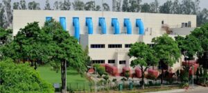
SCL Fab – Currently 0.18 Micron

Politics are the same everywhere, and so this process took some time, people with experience had to be recruited to run it, and a suitable (politically and geographically) location selected.  Eventually in the late 1970’s the Semiconductor Complex LTD was formed in the city of Mohali ( Chandigarh ) in the Punjab province of India.  SCL was to be the state supported enterprise to bring indigenous high end (LSI and above) semiconductor production to India.  Two things were needed to make this work: Technology, and People who were experts in that field.  SCL was tasked with going to Japan, America, and Western Europe in search of a company that would assist with the technology transfer, as well as finding some Non-Resident Indians who would be willing to come back to India to work on it.  Many Indians had high skill jobs in the industry outside of India, and it turned out convincing them to come back to help their country was a non-issue (though generous incentives were provided).  Getting the technology on the other hand was a bit more work.

The first trip of the technology transfer team of SCL was to Hitachi in Japan.  Negotiations with Hitachi were grueling, and while not unproductive, did not yield the results SCL wanted.  Hitachi was happy to license some designs to SCL, for a high fee and royalties, but did not want to immediately help create the 3-5 micron production fab that SCL envisioned.  Hitachi called thei ‘one step at a time’  whereas the Indians wanted to go all in from the start.  Hitachi agreed only to help (some) with a 5 micon process) and only to license products for digital clocks and watches.  The SCL team then turned to the United States, likely expecting similar results.

The chosen company in the USA was AMI (American Microsystems Inc), a company with 7-8 times the turnover of Hitachi.  AMI was at the time the largest maker of custom ICs in America, as well as a very large provider of second source ICs  (such as the 6800 and 9900 CPUs).  AMI’s CEO Roy Turner readily agreed to help SCL, much to the surprise of their negotiation team, and on the very first day offered SCL AMI’s 5 micro CMOS and NMOS processes, with the option to license their 3 micron CMOS and NMOS processes within 4 years of the agreement becoming effective.  AMI also offered SCL access to all of AMI’s standard products catalog, as well as the possibility of joint development of additional products, all at a simple 50/50 split.  AMI even offered to help with the technology export license that would be required by the US State Dept to transfer the fab tech to India.  The agreement was signed in April of 1981.

Read More »

Tags:
,

Posted in:
CPU of the Day

January 24th, 2020 ~ by admin

ARMing the Modems of the 1990’s

Racks of external modems at an ISP back in the day

Back in the 1990’s I worked at several ISP’s in my hometown.  These were the days of dial up, and by working at the ISP I got free dial up access which my family and I enjoyed.  We had several racks (white wire racks) of external modems for dial in.  This was the most common solution for smaller ISPs.  External modems were usually more reliable, cheap and easy to replace if/when they failed (and they did).  They got warm so it wasn’t uncommon to see a fan running to help move more air.  Surprisingly I could only find a few pictures of a such installations but you get that idea.

By the late 1990’s as dial in access and ISPs grew to be major concerns dial up solutions became much more sophisticated.  Gone were wire racks of modems and in were rackmount all in one dial in solutions.  These included boards that hosted dozens of modems on one PCB. with their own processing and management built in.  One of the largest companies for these solutions was Ascend Communications.  Their ‘MAX TNT’ modem solution once boasted over 2 million dial up ports during the 1990’s.  Such was Ascends popularity that they merged with Lucent in 1999, a deal that was the biggest ever at its time, valued at over $24 Billion ($37 Billion in 2020 USD). It wasn’t just traditional ISPs that needed dial up access, ATM’s and Credit Card processing became huge users as well.  It wasn’t uncommon to try to run a credit card at a store in the 1990’s and have to wait, because the machine got a busy signal.  The pictured Ascend board has 48 modems on a single PCB, and would be in a rack or case with several more boards, supporting 100s of simultaneous connections.

Ascen CSM/3 – 16x Conexant RL56CSMV/3 Chips provide 48 modems on one board.

Ascend’s technology was based primarily on modem chips provided by Conexant (Rockwell Semiconductor before 1999).  Rockwell had a long history of making modem controllers, dating back to the 1970’s.  Most of their modem controllers up through the 80’s and early 90’s were based on a derivative of the 6502  processor.  This 8-bit CPU was more the adequate for personal use modems up to 33.6kbaud or so, but began to become inadequate for some of the higher end modems of the 1990’s.  These ran at 56k, supported various voice. fax, and data modes and handled a lot of their own DSP needs as well.  Rockwell’s solution was to move to an ARM based solution, and integrate everything on chip.

One of the results of this was the Anyport Multiservice Access Processor. It was called the Multiservice Access Process because it handled, voice, data, 33.6/56k, ISDN, cellular, FAX and several other types of data access, and it did so in triplicate.  The RL56CSMV/3 supported 3 different ports on one chip.  The CSM3 series was the very first ARM cored device Rockwell produced.  Rockwell had licensed the ARM810 (not very common), the ARM7TDMI and a ‘future ARM architecture’ (which was the ARM9) back in January of 1997.  In less then two

Conexant RL56CSM/3 R7177-24 ARM7 (non-V version has no voice support)

years Rockwell had designed and released the first AnyPort device, remarkable at the time.  The CSM/CSMV used the ARM7TDMI running at 40MHz and made on a 0.35u process.  The CSM/CSMV has another interesting feature, and thats the backside of the chip….

Take a look of the backside of the 35mm BGA chip, the ball arrangement is very unusual!  There is a ring of balls around the outer edge and 4 squares of 16 balls inside of that.  This is a multi-die BGA package.  There are 4 die inside one BGA package, three dies for the 3 Digital Data Pumps (DDPs) and a seperate die for the ARM7 MCU (which is made on a different process then the mixed signal DDPs).  Most of the balls in the 16×16 squares are to be connected to GND, and used for thermal dissipation (dissipating heat via the main PCBs ground plane).  Its not uncommon to see multidie packages today, but a multi die BGA package in 1999 was fairly innovative.

Surprisingly many of these chips are still in service, in today’s world of high speed broadband connections there are still many who are stuck on dial up.  As recently as 2015 AOL was still serving 2.1 million dial up customs in the US (out of around 10 million dial up customers total), which was still netting the company nearly half a billion dollars a year (by far their largest source of revenue at the time.  There is also still plenty of other infrastructure that still rely on dial up, ISDN, and even FAX services that require end point connections like the CSMV so its end is probably still a long ways off.

Tags:
, ,

Posted in:
CPU of the Day

January 14th, 2020 ~ by admin

Barn Find MOS MCS6502 – A Restoration

ATARI Arcade BoardIn car collecting one of the ‘holy grail’ experiences is the ‘Barn Find’  finding and recovering a rare vehicle that has sat untouched, in some barn, or shed for some time.  They are often in rough, but original condition and can evoke much excitement.  As it turns out CPUs are not so different.  I recently purchased a very rough and very old ATARI Arcade board.

The pictures clearly showed it in terrible condition, with lots of oxidation and ‘stuff’ on it.  But it also had a white MOS 6502 processor.  These are some of the very first CPUs made by MOS and are rather desirable, as in addition to their use by ATARI, they were used in the very first Apple computer, the Apple 1.

When the board arrived it was clearly in bad shape, take a look at that nastiness.  What you can’t see, or rather smell, is the cow manure.  Clearly this board was in an actual barn at some point.  Probably relegated to such a retirement after serving in an Arcade parlor or bar for some time, either that or there was some bovin gaming going on.

You can see there is some oxidation on the lids of the various chips as well.  The ROMs and CPU are in sockets.  These sockets are nice, they are not a machine socket but rather a LIF, Low Insertion Force Socket, that helps as the pins on these chips are very delicate, and very possibly corroded.

Before attempting to remove the MCS6502 its best to see what I am working with, so I pulled some of the ROMs nearest to the 6502 to see how their pins looks and how easy they came out of their sockets.  They came out with not a lot of effort but you can see there is some oxidation on the pins.  What we do not want is the pins to be rusted TO the socket and then break off from the forces needed to remove the chip from the socket.

To help mitigate this risk I used some penetrating oil on the pins in the socket.  It seems strange to be squirting oil in the socket but it works.  It will help penetrate the rust and decrease the force needed to remove the 6502. After adding the oil I let the board sit on my heater in my office for several hours.  This helps the oil penetrate, as well as made my office smell like Deep Creep and cow manure, all in a days work.

Then I very gently work on removing the 6502, testing how tight it is and working it out from both ends.  It comes looses with very little drama, hopefully with all its pins intact….

Read More »

Tags:
, ,

Posted in:
How To

December 27th, 2019 ~ by admin

RIP Chuck Peddle: Father of the 6502

Original MOS 6501 Processor from 1975 – Designed by Chuck Peddle.

On December 15th one of the truly greats of processor design passed away at age 82.  Chuck Peddle, born in 1937, before semiconductors were even invented, designed the 6502 processor back in 1974.  The 6502 (originally the 6501 actually) went on to become one of the most popular and widely used processors of all time.  It powered the likes of the Apple 1, Commodores, ATARIs and hundred of others.  It was copied, cloned, and expanded by dozens of companies in dozens of countries.  It was so popular that computers were designed to use it in the Soviet Union, eventually making their own version (Pravetz in Bulgaria).

Sitronix ST2064B – Based on the 65C02 – Core is visible in the upper right of the die. (photo by aberco)

The 6502 was a simple but useful 8-bit design, which meant that as time went along and processors migrated to 16 32 and 64-bits and speeds jumped from MHz to GHz the venerable 6502 continued to find uses, and be made, and expanded.  Chuck continued to be involved in all things 6502 until only a few years ago, designing new ways to interface FLASH memory (which hadn’t been invented when he designed the 6502) to the 6502.

The chips themselves, now in CMOS of course, continue to be made to this day by Western Design Center (WDC) and the 65C02 core is used in many many applications, notably LCD monitor controllers and keyboard controllers.  We can hope that the 6502 will have as long of life as Mr. Peddle, though I woud wager, that somewhere, somehow , in 2056 a 6502 will still be running.

Tags:
,

Posted in:
Museum News

June 1st, 2019 ~ by admin

All Boxed up: Retail Boxed CPU’s

NIB MOS 6502 CPU

New In Box MOS MCS6502 CPU from 1975 (Michael Steil – pagetable.com)

Today most all processors are permanently installed in their device (soldered in) or were taken from a bulk tray and installed by the OEM such as Dell or HP.  AMD has, at least with their higher end CPU’s gotten quite creative with the marking on the chip itself, and both AMD and Intel still offer some pretty amazing retail packaging for their enthusiast processors (the i9 in a dodecahedron package is pretty cool).  There was a time when almost all processors were available in retail packaging.  This was the time of physical computer shops, largely bypassed now by the Internet, where the packaging of a processor helped sell it.

I collect such New In Box (NIB) processors as they are pretty need to see the branding/marketing that went with the CPU’s of years past, and was reminded of this when I saw perhaps one of the oldest NIB CPU’s I have ever seen on Michael Steil’s pagetable.com blog.  An original MOS 6502 processor from 1975 in its original shipping box, as close to NIB as one can get.  MOS’s packaging would make Apple proud with its simplicity and design keeping everything tidy and the MCS6502 visible as soon as the box is opened (I am happy they didn’t use miserable black foam either, so the CPU is pristine after 45 years).  Even the original invoice is included.  $25 for the CPU ($118 in 2019 dollars) and $10 (nearly half the cost of the CPU ($47 in 2019)) for documentation)

Cyrix 83D87 386 FPU

Cyrix 83D87 386 FPU Bundled with Borland Quattro PRO Spreadsheet software (a big thing back in 1992)

Intel started offering retail boxed CPUs with the 8087 coprocessor.  This was really the first chip designed as a user upgrade to their PC (a new thing back then).  Before this Intel’s closest thing to a NOB was University Kits or Dev Kits for various chips/processors.  With the introduction of the PC, and the many thousands of beige box clones that followed, people themselves began buying processors and building computers for themselves at a much greater pace then before.  There was many companies making compatible processors at the time so packaging helped set them apart.  This began with upgrade products, math coprocessors for the 808x, 286 and 386 were the most common (by Intel, AMD, IIT, ULSI. Cyrix and more), but eventually processors themselves started getting the NIB treatment, Intel made OverDrive processors (still technically an upgrade product) for the 486. followed by actual Pentium CPUs in the retail box. By the late 1990’s everything from Celerons to Xeon server processors could be had in Retail box.  Buying a retail boxed Xeon for your rackmount server seems like an odd thing to do, but apparently Intel figured it would need to be done.

Quad AMD Opteron 6128s in Retail Box

Quad AMD Opteron 6128s in Retail Box

Other companies such as AMD, Cyrix and VIA made NIB processors but they are much less common, and in a lot of ways more interesting.  AMD made retail Durons, Athlons, and Opterons, and in one of the most unusual things I have seen for a NIB, an actual 4-pack of Opteron 6128s (pictured). The Opteron 6128 is a 8 core Magny-Cours server processor introduced in 2009 and cost $266 each at that time.  This NIB set is dated late 2011, so would probably be a bit cheaper, but still $800 or so, and the large SWATX motherboards needed to run 4 socket G34 processors require somewhat special cases and PSU’s, but at least you can have  a half terabyte of RAM.  Inside the retail box is 4 smaller boxes, each containing an Opteron 6128 CPU, installation instructions, warranty info, and a case badge (you get 4 total case badges).  It seems this packaging was designed to support different configurations (probable a single Opteron 6128, and duals).

Tags:
, ,

Posted in:
CPU of the Day

March 11th, 2015 ~ by admin

Emulating the Intel 8080 on a MOS 6502

Pagetable.com has in interesting post about emulators, specifically one created in 1978 to run Intel 8080 code on a 6502.  While emulators today are fairly common, such as running Nintendo (6502) games on a PC, or In Circuit Emulators for development, an 8-bit cross architecture emulator is certainly different.  Especially since the 8080 and 6502 were so vastly differing.  Certainly a useful tool for teaching oneself a new architecture, and as they were coming out rather rapidly in the 1970’s knowing more then one was a worthy investment.

Todays equivalent perhaps would be emulating a PIC on a 8051.  Perhaps someone will give it a try?

Tags:
,

Posted in:
Processor News

August 3rd, 2013 ~ by admin

MOS Technology MCS6501 Processor

MOS MCS6501 - November 1975

MOS MCS6501 – November 1975

One of the classic stories of the 1970’s microprocessor boom times was that of MOS Technologies at WESCON (Western Electronics Show and Convention) on September 16th 1975 in San Francisco.  MOS Technology was a newcomer to microprocessors.  They had with them two brand new processor design, the MCS6501 and the MCS6502 which they hoped to sell on the floor at Wescon, for $20 and $25 each.  However Wescon forbid sales on the convention floor, so quick thinking by MOS Technologies Chuck Peddle directed people to a hotel room, where “the beer was free and chips were $25.”  In the room were jars of 6501 and 6502 processors, to give them impression that these were in full production.  In reality the bottoms of the jars were filled with defective parts.  It was no matter, the 6500 series was a huge hit, led largely by its availability, low price and marketing to everyone (not just ‘big corporate users’).  The 6500, and specifically the 6501 have an interesting story leading up to that fateful day at WESCON.

Motorola XC6800B - July 1975 - Pre-production part, not something MOS bothered with.

Motorola XC6800B – July 1975 – Pre-production part, not something MOS bothered with.

It begins at Motorola, where Chuck Peddle, Bill Mensch and several others were employed in the early 1970’s design the MC6800 processor and its peripherals.  The 6800 was not a bad design, it was however, very expensive, a development board for it costing over $300.  Chuck worked largely as the 6800 system architect, ensuring all the ICs worked well together and were what was needed to meet customers needs.  He attended many calls to potential clients and noted that many were turned off by one thing, price.  With that in mind he sought out to build a lower cost version of the 6800 using some of the newer processes available (specifically depletion mode NMOS vs the enhancement mode of the 6800).  Motorola management wouldn’t hear it, they wanted nothing to do with a lower cost processor available to the masses.  And with that, Chuck, Bill and over half the 6800 team left.

Read More »

Posted in:
CPU of the Day

April 7th, 2011 ~ by admin

The Commodore is back!

Commodore USA has started taking pre-orders of its newly revamped Commodore 64 Home Entertainment system.   Of course this version comes with Blu-Ray and a dual core Intel (gasp!) processor running a version of Ubuntu Linux, it will include a Commodore OS 1.0 emulator, which should run all your favorite C64 6502 based games.

Commodore USA C64 - 1.8 Dual core Atom - 2GB RAM

The Original C64 had 64k of RAM, the Intel Atom D525 has 112k of just L1 cache.  At least the die size is similar :).
Commodore USA is also making modern version of the VIC computers for your enjoyment, albeit in slightly modified cases.

Tags:
,

Posted in:
Just For Fun

February 2nd, 2011 ~ by admin

How many Commodore 64 computers were really sold?

Production numbers of vintage technology have always been a somewhat mysterious subject.  How many 4004 processors did Intel actually make? I am not even sure Intel knows.  Unlike modern car companies who can track production numbers down to the shift of the day it was made, computer companies of the 70’s and 80’s were rather fast and loose with record keeping.

Thankfully with some research, serial numbers and some math (the famous tank equation) Michael Steil of Pagetable.com came up with what appears to be a very good estimate of Commodore 64 production.  12.5 million units, somewhat less then other numbers that have been thrown around, but backed by research and supported by math.  Read how he came to the conclusion here.

Tags:
,

Posted in:
Research

November 23rd, 2010 ~ by admin

Another Apple 1, Another Quarter Million Dollars

In September a Apple 1 computer with a few accessories sold for $23,000.  Christie’s has just auctioned off an early (first run) Apple 1, with invoice, shipping box, letter from ‘Steven Jobs’ and many accessories for a staggering $213,600.  This would have been one of the original PCB’s, sold without components and later assembled by someone else.  The main CPU is of course a 6502 but in this case a R6502P by Rockwell made in late 1981.

Complete Apple 1

What made this one so much more valuable?  The documentation and original box.  Whoever bought it should however replace the CPU with a white ceramic MOS 6502 to preserve the beauty of the original Apple 1.

Tags:
,