June 5th, 2022 ~ by admin

CPU of the Day: P.A. Semi PA6T PowerPC

When Apple bought P.A. Semi back in 2008 it was the beginning of the era of the iPhone, and their was much speculation as to why Apple was buying a company that made low power high performance PowerPC processors.  Especially since the iPhone ran on ARM and the Mac had moved from PowerPC to x86.

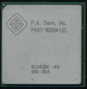
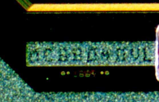
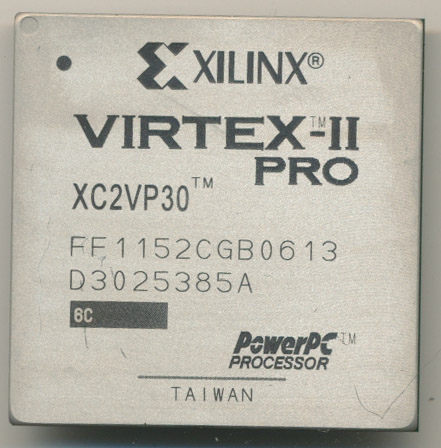
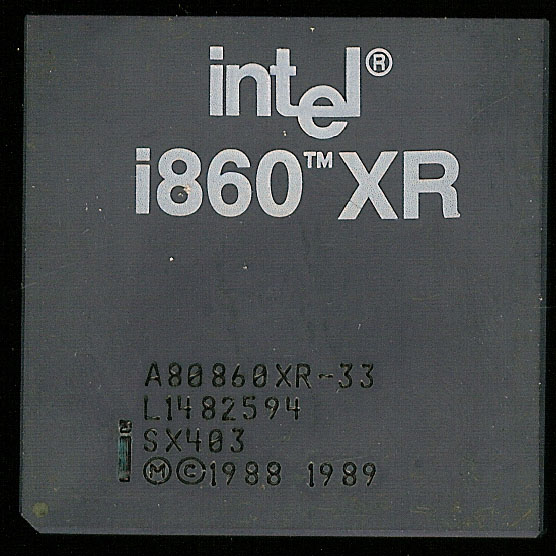
P.A. Semi PA6T-1682M

P.A. Semi was started in 2003 by Daniel Dobberpuhl (who passed away in 2019).  Dobberpuhl was one of the truly greats of microprocessor design, with a career starting at DEC on the T-11 and MicroVAX, before helping DEC transition to the Alpha RISC design (21064).  It was Dobberpuhl who started the design center in Pal Alto (where P.A. Semi would later take its name from) that designed the DEC StrongARM processor.  A processor that was later purchased by Intel and became the XScale line of ARM processors.

After Intel bought the StrongARM line, he then helped start SiByte, making MIPS based RISC CPUs, and continued to do so when SiByte was purchased by Broadcom. So when he started P.A. Semi it was less about PowerPC and more about RISC, PowerPC just happened to be the architecture they chose to use.  The design team had extensive experience on a variety of CPU architectures, including SPARC, Itanium, and the early Opterons.  You can see why this acquisition was so attractive to Apple.
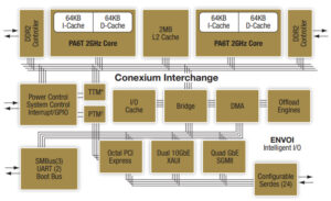
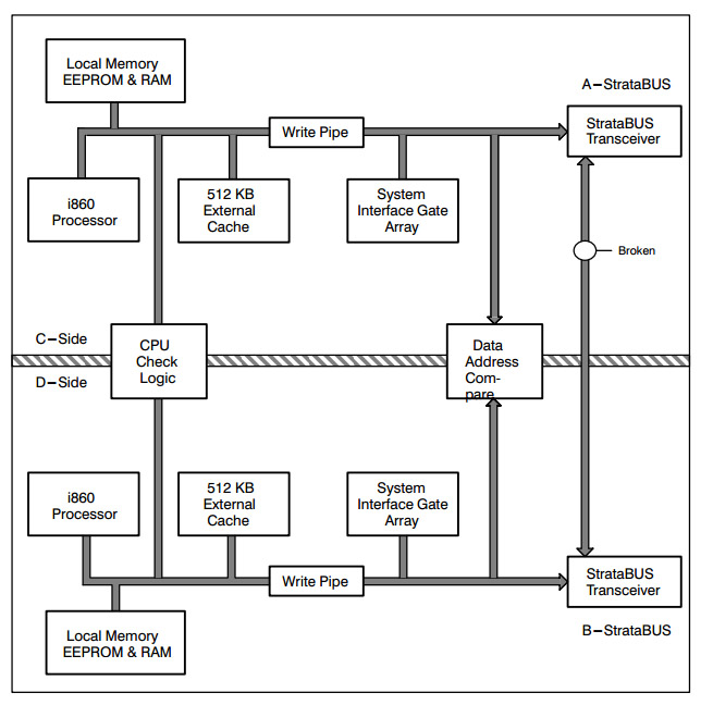
PA6T block diagram

In the few years (2003-2008) from when P.A. was founded to when Apple took them over, they did design, market, and sell a PowerPC processor line called PWRficient based on what they called the PA6T core.  The PA6T-1682M was a Dual core PowerPC processor (the 13xxM was the single core version) with each core running at up to 2GHz with 64K of L1 Instruction cache and 64K of L1 Data cache.  They were fab’d on a 65nm process by TI and ran at 1.1V.  The L2 cache was scalable and shared amongst the cores.  In the 1682M this was a 2M 8-way cache with ECC.  One of the most useful features was their clock stepping.  They could drop to 500MHz at only a few watts per core, and then back up to the full 2GHz in 25us.

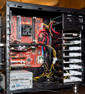
AmigaOne X1000 (made by Aeon) PA6T-1682M

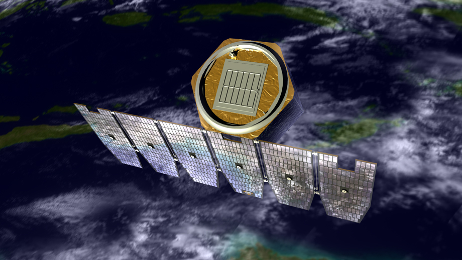
The PA6T was only on the marked for a few months (from the end of 2007 to April 2008) before Apple bought them for $300 million, but in this time P.A. Semi had numerous design wins.  Amiga selected it for use in the AmigaOne X1000 computer.  The AmigaOne did not hit market until 2011, which means that while P.A. Semi was bought and completely under control of Apple, they still continued to make, support, and supply their previous customers with the 1682M CPU.  Certainly Amiga wouldn’t be big enough to push Apple to continue making a chip?

They were not, but others were, and the PA6T was such a great processor that it had been selected and designed in to many computer system used by US Defense contractors, and if anyone doesn’t like change, its Defense contractors, so with some prodding by the US Dept of Defense Apple continued to make (or rather have TI make) the PA6T processors.  Curtis-Wright had designed the PA6T into their new CHAMP-AV5 DSP VME64 board, which was used for signals processing across numerous military applications.  They also also used the PA6T (at 1.5GHz) in the VPX3-125 SBC. Themis computers, NEC, Mercury and others designed in the PA6T. Extreme Engineering, another maker of PA6T based boards, referred to the design as ‘ground breaking.’

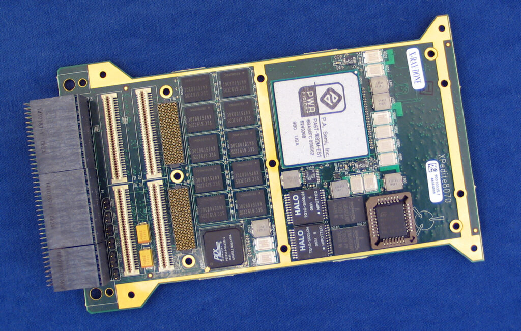
Extreme Engineering XPedite8070 SBC

It would have been interesting to see what P.A. Semi could have achieved had they not been gobbled up by Apple.  Clearly we see the results of the talent of the P.A. team in what Apple was able to accomplish with their A-series processors, but clearly P.A. had something special for the PowerPC architecture as well.

Tags:
, ,

Posted in:
CPU of the Day

November 1st, 2019 ~ by admin

CPU of the Day: Motorola MC68040VL

Motorola MC68040VL

A month or so ago a friend was opening up a bunch of unmarked packages, and taking die photos and came across an interesting Motorola.  The die looked familiar, but at the same time different.  The die was marked 68040VL, and appeared to be smaller version of the 68040V.  The Motorola 68040V is a 3.3V static design of the Motorola MC68LC040 (It has dual MMUs but lacks the FPU of the 68040).  The 68040V was made on a 0.5u process and introduced in 1995.  Looking closely at the mask revealed the answer, in the form of 4 characters. F94E

Motorola Mask F94E – COLDFIRE 5102

Motorola uses mask codes for nearly all of their products, in many ways these are similar to Intel’s sspecs, but they are more closely related to actual silicon mask changes in the device.  Multiple devices may use the same mask/mask code just with different features enabled/disabled.  The Mask code F94E is that of the first generation Motorola COLDFIRE CPU, the MCF5102.  The COLDFIRE was the replacement for the Motorola 68k line, it was designed to be a 32-bit VL-RISC processor, thus the name 68040VL for VL-RISC. .  VL-RISC architectures support fixed length instruction (like a typical RISC) but also support variable length instructions like a traditional CISC processor.  This allows a lot more code flexibility and higher code density.  While this may be heresy to RISC purists it has become rather common.  The ST Transputer based ST20 core is a VL-RISC design, as is the more modern RISC-V architecture.  The COLDFIRE 5102 also had another trick, or treat up its sleeve.  It could execute 68040 code.

Read More »

March 1st, 2019 ~ by admin

CPU of the Day: UTMC UT69R000: The RISC with a Trick

UTMC UT69R000-12WCC 12MHz 16-bit RISC -1992

We have previously covered several MIL-STD-1750A compatible processors as well as the history and design of them.  As a reminder the 1750A standard is an Instruction Set Architecture, specifying exactly what instructions the processor must support, and how it should process interrupts etc.  It is agnostic, meaning it doesn’t care. how that ISA is implemented, a designers can implement the design in CMOS, NMOS, Bipolar, or anything else needed to meet the physical needs, as long as it can process 1750A instructions.

Today we are going to look at the result of that by looking at a processor that ISN’T a 1750A design.  That processor is a 16-bit RISC processor originally made by UTMC (United Technologies Microelectronics Center).  UTMC was based in Colorado Springs, CO, and originally was formed to bring a semiconductor arm to United Technology, including their acquisition of Mostek, which later was sold to Thomson of France. After selling Mostek, UTMC focussed on the military/high reliability marked, making many ASICs and radhard parts including MIL-STD-1553 bus products and 1750A processors.  The UT69R000 was designed in the late 1980’s for use in military and space applications and is a fairly classic RISC design with 20 16-bit registers, a 32-bit Accumulator, a 64K data space and a 1M address space.  Internally it is built around a 32-bit ALU and can process instructions in 2 clock cycles, resulting in 8MIPS at 16MHz.  The 69R000 is built on a 1.5u twin-well CMOS process that is designed to be radiation hardened (this isn’t your normal PC processor afterall).  In 1998 UTMC sold its microelectronics division to Aeroflex, and today, it is part of the English company Cobham.

UTMC UT1750AR – 1990 RISC based 1750A Emulation

UTMC also made a 1750A processor, known as the UT1750AR, and if you might wonder why the ‘R’ is added at the end.  The ‘R’ denotes that this 1750A has a RISC mode available.  If the M1750 pin is tied high, the processor works as a 1750A processor, tied low, it runs in 16-bit RISC mode.  How is this possible? Because the UT1750AR is a UT69R000 processor internally.  Its the same die inside the package, and the pinout is almost the same (internally it may be but that’s hard to tell).  In order for the UT1750AR to work as a 1750A it needs an 8Kx16 external ROM.  This ROM (supplied by UTMC) includes translations from 1750A instructions to RISC macro-ops, not unlike how modern day processors handle x86.  The processor receives a 1750A instruction, passes it to the ROM for translation, and then processes the result in its native RISC instructions.   There is of course a performance penalty, processing code this way results in 1750A code execution rates of 0.8MIPS at 16MHz, a 90% performance hit over the native RISC.  For comparison sake, the Fairchild F9450 processor, also a 1750A compatible CPU, executes around 1.5MIPS at 20MHz (clock for clock, about 30% faster), and thats in a power hungry Bipolar process, so the RISC translation isn’t terrible for most uses.

NASA Aeronomy of Ice in the Mesosphere – Camera powered by RISC

By today’s standards, even of space based processors, the UT69R000 is a bit underpowered, but it still has found wide use in space applications.  Not as a main processor, but as a support processor, usually supporting equipment that needs to be always on, and always ready.  One of the more famous mission the UT69R000 served on was powering the twin uplink computers for the DAWN asteroid mission (which only this year ended).  It was also used on various instrumentation on the now retired Space Shuttles. The CPU also powered the camera system on the (also retired) Earth Observing-1 Satellite, taking stellar pictures of our planet for 16 years from 2000-2017.  Another user is the NASA AIM satellite that explores clouds at the edge of space, originally designed to last a couple years, its mission which started in 2007 is still going.  The

JAXA/ESA Hinode SOLAR-B Observatory

cameras providing the pretty pictures are powered by the UT69R000.  A JAXA/ESA mission known as SOLAR-B/Hinode is also still flying and running a Sun observing telescope powered by the little RISC processor.

There are many many more missions and uses of the UT69R000, finding them all is a bit tricky, as rarely does a processor like this get any of the press, its almost always the Command/Data Processor, these days things like the BAE RAD750, and LEON SPARC processors, but for many things in space, and on Earth, 16-bits its all the RISC you need.

October 12th, 2018 ~ by admin

Xilinx gets ARMed up for Free

Xilinx Virtex II Pro FPGAs from the 2000’s included embedded PowerPC processor cores.

Recently ARM announced they would be providing IP for the Cortex-M1 and M3 cores for free for users of Xilinx FPGA’s.  The Cortex-M1 and M3 are some of the most basic ARM cores, taking 12-25,000 gates for the Von Neumann architecture M1 and around 43,000 for the full up Harvard architecture M3 (with full ARM THUMB instruction set support).  Xilinx already offers FPGAs/SoCs with built in ARM cores, the SYNQ series is available with a variety of high end ARM cores such as the Cortex-A53 and the RF focused R5 core.  These obviously are fairly high gate county, and cost cores, where as the M1 and M3 cores are being provided without license, and without any royalties.  Drop in the IP into your FPGA design and go.

ARM and Xilinx say this is to meet the needs of their customers, who want to be able to use the same ARM architecture in their FPGA designs as in ASICs etc, and at the lowest investment in time and cost.  This certainly makes sense, having a free ARM core is better then a low cost ARM core, and removing the ‘paperwork’ hassle helps, but that’s probably not the only reason ARM is doing this, and doing it specifically for Xilinx.

There are a couple other things at play here, ARM Mx cores are basic RISC processors, used for when you just need to get some basic processing done, no frills, low power, and easy to use.  It turns out that’s a market that is now seeing some competition from the SiFive RISC-V core.  This is a basic, easy to use RISC core, that is synthesizable into ASICS, and FPGAs, and comes with a one time low cost license fee and no royalties.  Its being used by such heavyweights as Nvidia, and could threaten the Cortex-Mx domain, so it makes sense for ARM to offer, essentially their introductory processor core, for free, as a way to sway people to the ARM ecosystem.  But why Xilinx?

Perhaps Xilinx is just the start of ARM’s plans, Xilinx is one of the biggest providers of FPGAs in the world so certainly that will help keep people in the ARM. Xilinx infact, already has a drop-in 32-bit RISC processor core available to all their customers, the MicroBlaze and PicoBlaze, of their own design.  There are also drop in 80C186 cores, MCS-51 cores, the LEON SPARC core and many others. The other big name in FPGAs is Altera, a company that has competed with Xilinx for the better part of 30-years and was, in June of 2015 bought by none other then Intel.

Altera has had a close relationship with Intel since the 1980’s when Intel first started assisting Altera with fab’ing their PLDs.

This gave Altera greater access to Intel’s fab/engineering prowess, but also to all of Intel’s IP.  Is Intel going to offer free ARM cores on Altera FPGAs (the Stratix/Arria series does include hard Cortex-A9/A53 cores already)?  It seems unlikely that they would work to support their architectural competitor any more then they have to.  It is more likely that Intel would offer some form of 32-bit x86 processor core for their FPGAs.  Now x86 isn’t exactly known for low gate counts, but it is possible.  Currently softcore 8086 and 80186 processor (the Turbo86 and Turbo186) are 22,000 and 30,000 gates respectively, really a rounding error in FPGAs that now have millions of gates. More and more, FPGAs are becoming less FPGA like, and more ‘configurable processor’ like.

June 5th, 2017 ~ by admin

SiFive FE310: Setting The RISC Free

SiFive FE310 RISC-V Processor. Early LSI SPARC Processor for size comparison. Both are based on U.C. Berkeley RISC designs.

The idea of RISC (Reduced Instruction Set Computer) processors began in education, specifically University of California, Berkeley in the early 1980’s, and it was out universities that some of the most famous RISC designs came.  MIPS, still in use today, started life as a project at Stanford University, and SPARC, made famous by Sun, and now made by Oracle and Fujitsu, started life as a Berkeley University project.  Universities have continued to work with RISC architectures, for research and teaching.  The simplicity of RISC makes them an ideal educational tool for learning how computers/processors function at their basic levels.

By the late 1980’s RISC had begun to become a commercial revolution, with nearly every player having their own RISC design.  AMD (29k), Intel (i960), HP (PA-RISC), Weitek (XL8000), MIPS, SPARC, ARM, Hitachi (SH-RISC), IBM (POWER), and others offered their take on the RISC design.  Most were proprietary, while a few were licenseable, none were open architectures for anyone to use.

Unfortunately, outside of the university, RISC processors are not as simple.  The architectures, and their use may be, but licensing them for the design is not.  It can often take more time and effort to license a modern RISC processor then it does to actually implement it.  The costs to use these architectures,both in time and money often prohibit their very use.

SiFive FE310 – Sample Donated by SiFive. Full 32-bit RISC on a 7.2mm2 die in a ~36mm2 package

It is out of this that SiFive began.  SiFive was founded by the creators of the first commercially successful open RISC architecture, known as RISC-V.  RISC-V was developed at Berkeley, fittingly, in 2010 and was designed to be a truly useful, general purpose RISC processor, easy to design with, easy to code for, and with enough features to be commercially useful, not limited to the classroom.  It is called the RISC-V because it is the fifth RISC design developed at Berkeley, RISC I and RISC II being designed in 1981, followed by SOAR (Smalltalk On A RISC) in 1984 and SPUR (Symbolic Processing Using RISC) in 1988.  RISC-V has already proved to be a success, it is licensed freely, and in a way (BSD license) that allows products that use it to be either open, or proprietary.  One of the more well known users is Nvidia, which announced they are replacing their own proprietary FALCON processors (used in their GPUs and Tegra processors) with RISC-V.  Samsung, Qualcomm, and others are already using RISC-V.  These cores are often so deeply embedded that their existence goes without mention, but they are there, working in the background to make whatever tech needs to work, work.

The RISC-V architecture supports 122 instructions, 98 of which are common to almost all prior RISC designs and 18 common to a few.  Six completely new instructions were added to handle unique attributes of the architecture (using a 64-bit Performance Register in a 32-bit arch.) and to support a more powerful sign-injection instruction (which can be used for absolute value, among other things). It uses 31 32-bit registers (Register 0 is reserved for holding the constant ‘0’) with optional support for 32 floating point registers.  True to the RISC design, it is a pure Load/Store processor, the only accesses to memory are via the Load/Store instructions.

Intel 4004 with 5 SiFive RISC Processors. The 4004 was meant for a calculator. The FE310 is meant for whatever your mind may dream up.

SiFive is unique among RISC IP companies.  They not only license IP but also sell processors and dev boards.  The FE310 (Freedom Everywhere 310) is a 320MHz RISC-V architecture with 16K of I-cache and 16K of scratchpad RAM fabbed by TSMC on a 180nm process. Even on this process, which is now a commodity process, the FE310’s efficient design results in a die size of only 2.65mm x 2.72mm.  On a standard 200mm wafer , this results in 3500 die per wafer, greatly helping lower the cost.  Its an impressive chip, and one that is completely open source.  What is more impressive is licensing SiFive cores, it is a simple and straightforward process.  The core (32 bit E31 or 64-bit E51) can be configured on SiFive’s site, with pricing shown as you go.  The license is a simple 7 page document that can be signed and submitted online.  Pricing starts at $275,000 and is a one time fee, there are no continuing royalty payments.  The entire process can be completed in a week or less.

In comparison, ARM, the biggest licensor of RISC processors, does not publish pricing, charges 1-2% royalties on every chip made, and has a license process that can take over a year.  The base fees start at around $1 million and go into the 10’s of millions, depending on how you want to use the IP, where it will be, and for how long.  For many small companies and users this is simply not feasible, and it is these smaller users that SiFive wishes to work with.  Licensing a processor for the next great tech, should not be the hurdle that it has become.  Many great ideas never make it to fruition due to these roadblocks.  We look forward to finding SiFive processors and cores in all sorts of products in the future.

Thanks to SiFive for their generous donation of several FE310 processors to the CPU Shack Museum.

Tags:
, , , ,

Posted in:
CPU of the Day

January 28th, 2017 ~ by admin

Stratus: Servers that won’t quit – The 24 year running computer.

Stratus XA/R (courtesy of the Computer History Museum)

Making the rounds this week is the Computer World story of a Stratus Tech. computer at a parts manufacturer in Michigan.  This computer has not had an unscheduled outage in 24-years, which seems rather impressive.  Originally installed in 1993 it has served well.  In 2010 it was awarded for being the longest serving Stratus computer, then being 17 years.  Phil Hogan, who originally installed the computer in 1993, and continues to maintain it to this day said in 2010  “Around Y2K, we thought it might be time to update the hardware, but we just didn’t get around to it”  In other words, if it’s not broke, don’t fix it.

Stratus computers are designed very similar to those used in space.  The two main difference are: 1) No need for radiation tolerant designs, let’s face it, if radiation tolerance becomes an issue in Michigan, there are things of greater importance than the server crashing and 2) hot swappable components.  Nearly everything on a Stratus is hot-swappable.  Straus servers of this type are based on an architecture they refer to as pair and spare.  Each logical processor is actually made from 4 physical CPU’s.  They are arranged in 2 sets of pairs.

Stratus G860 (XA/R) board diagram. Each board has 2 voting i860. (the pair) and each system has 2 boards (the spare).  The XP based systems were similar but had more cache and supported more CPUs.

Each pair executes the exact same code in lock-step.  CPU check logic checks the results from each, and if there is a discrepancy, if one CPU comes up with a different result than the other, the system immediately disables that pair and uses the remaining pair.  Since both pairs are working at the same time there is no fail-over time delay, it’s seamless and instant.  The technician can then pull the mis-behaving processor rack out and replace it, while the system is running.  Memory, power supplies, etc all work in similar fashion.

These systems typically are used in areas where downtime is absolutely unacceptable, banking, credit card processing, and other operations are typical.  The exact server in this case is a Stratus XA/R 10.  This was Stratus’s gap filler.  Since their creation in the early 1980’s their servers had been based on Motorola 68k processors, but in the late 1980’s they decided to move to a RISC architecture and chose HP’s PA-RISC.  There was a small problem with this, it wasn’t ready, so Stratus developed the XA line to fill in the several years gap it would take. The first XA/R systems became available in early 1991 and cost from $145,000 to over $1 million.

Intel A80860XR-33 – 33MHz as used in the XA/R systems. Could be upgraded to an XP.

The XA is based on another RISC processor, the Intel i860XR/XP.  Initial systems were based on 32MHz i860XR processors.  The 860XR has 4K of I-cache and 8K of D-cache and typically ran at 33MHz.  Stratus speed rating may be based on the effective speed after the CPU check logic is applied or they have downclocked it slightly for reliability. XA/R systems were based on the second generation i860XP.  The 860XP ran at 48MHz and had increased cache size (16K/16K) and had some other enhancements as well.  These servers continued to be made until the Continuum Product Line (Using Hewlett Packard “PA-RISC” architecture) was released in March of 1995.

This type of redundancy is largely a thing of the past, at least for commercial systems.  The use of the cloud for server farms made of hundreds, thousands, and often more computers that are transparent to the user has achieved much the same goal, providing one’s connection to the cloud is also redundant.  Mainframes  and supercomputers are designed for fault tolerance, but most of it is now handled in software, rather than pure hardware.

Posted in:
Museum News

April 14th, 2016 ~ by admin

DEC NVAX++ NV5: The End of VAX

DEC NVAX 21-34457-05 246B - 1992  -71MHz

DEC NVAX 21-34457-05 246B – 1992 -71MHz

About a year ago we covered the DEC RIGEL VAX Processor.  After The RIGEL DEC moved to make a single chip VAX processor that would include the CPU, FPU, and cache controller on one single die.  Work on the design began in 1987, and first silicon shipping in 1991.  Performance ended up being as good or better then the very high end VAX 9000 systems (implemented in ECL logic).

The original NVAX processor was made on a 0.75u 3-Layer CMOS process (DEC CMOS-4) and contained 1.3 million transistors in a 339 pin CPGA package.  Initial clock speed, in 1991 was 71MHz.  NVAX was then the fastest CISC processor made.  Speeds ramped up to 90.9MHz at the high end and a lower end of 62.5MHz. The first NVAX models were identified as 246B and 246C. Later versions, made well into 1996, were made on the CMOS-4S process, a 10% shrink to 0.675u and were labeled 1001C.

Internally NVAX was very familiar, the FPU was largely reused directly from RIGEL.  The NVAX also maintains the 4-phase clocking scheme from RIGEL, but moves the clock generator on chip. It also maintained the 2K of on die instruction cache from RIGEL, but added a 8K data/instruction mixed cache as well.  An L2 cache was supported in sizes of 256K 512K 1M or 2M, and located off chip.  The NVAX continued the 6-stage pipeline of RIGEL with some enhancements.  One of the greatest performance enhancements over RIGEL is the handling of pipeline stalls.  In the RIGEL pipeline, a stall in one stage would stall the entire pipe line, whereas on NVAX, in most cases, a stall in one stage does not prevent the other stages from continuing.

At nearly the same time as the development of the NVAX DEC was also developing a competitor to MIPS, a RISC architecture.  This new RISC architecture was codenamed EVAX, for Enhanced VAX, and was a purely RISC architecture that could run translated VAX CISC code with very little performance penalty.  It did however borrow from VAX, like the NVAX, EVAX used the FPU from the RIGEL. DEC went on to brand the EVAX as Alpha AXP, to separate it from the VAX line, though its internal naming of EV4, EV5 etc was left intact, as the last remnant of VAX.

DEC 2140568-02 299D NVAX++ 170.9MHz - 1996 - from a VAX7800

DEC 21-40568-02 299D NVAX++ 170.9MHz – 1996 – from a VAX7800

Having two high performance processor types at the same time left DEC in a bit of a dilemma so they created a third, known as the NVAX+ (DEC 262D).  The NVAX+ was originally made on the same CMOS-4 process as the NVAX and ran at 90.9MHz.  The NVAX+ was meant to be a bridge between the VAX line and the Alpha AXP.  It was a NVAX core, wrapped in an EVAX (Alpha AXP) external interface, it was made in the same 431PGA as the Alpha 21064 and was pin for pin compatible, the same board could be used for either.  It supported more L2 cache then the NVAX, supporting six cache sizes (4MB, 2MB, 1MB, 512KB, 256KB, 128KB),

In 1994 the NVAX+ was shrunk to the DEC CMOS-5 4-Layer 0.5 micron process resulting in the NVAX++ (DEC 299D) which ran from 133-170.9MHz.  These speeds continued to be the fastest CISC processors until Intel released the Pentium Pro at 180 and 200MHz in 1996.  Ultimately Intel’s dominance, and the coming dominance of RISC performance were the writing on the wall, and the VAX, and not long after it DEC itself were doomed to reside in the history books.  By 1997 The NVAX++ was off the market.  In 1997 the DEC Alpha team was operating out of offices owned by Intel (who also took over DEC’s fab’s), and in 1998 the remains of DEC, and the Alpha team, were bought by Compaq. And by 2004 Alpha was phased out in favor of Itanium (a now rather ironic decision by HP/Compaq).


Tags:
, , ,

Posted in:
CPU of the Day

September 15th, 2013 ~ by admin

Compaq 21364 Processor – The Omega of the Alpha

Compaq 21364 Alpha Prototype - 2002

Compaq 21364 Alpha Prototype – 2002

The DEC Alpha was one of the fastest processors of the 1990’s. The original 21064, manufactured in CMOS, rivaled the fastest ECL processors and blew away most everything else.  Clock speeds were 150-200MHz (eventually hitting 275MHz) at a time when a standard Intel PC was hitting 66MHz, at the very top end. It was manufactured on a 0.75u process using 1.68 million transistors.  The Alpha was a 64-bit RISC design, at a time when 16-bit computing was still rather common.  This gave the architecture a good chance at success and a long life.

The 21064 was followed by the 21164 in 1995 with speeds up to 333MHz on a 0.5u process, now using 9.3million transistors.  It added an on die secondary cache (called the Scache) of 96KB as well as 8KB instruction and Data caches.  These accounted for 7.2 million transistors; the processor core itself was only around 2.1 million, a small increase over the 21064.  At the time the main competition was the Pentium Pro, the HP PA8800 and the MIPS R10000.  Improved versions were made by both DEC and Samsung, increasing clock speeds to 666MHz by 1998.

In 1996 DEC released the next in the series, the 21264.  The 21264 dropped the secondary cache from the die, and implemented it off chip (now called a Bcache).  The level 1 caches were increased to 64KB each for instruction and data resulting in a transistor count rise to 15.2 million, 9.2 million of which were for the cache, and the branch prediction tables.  Frequency eventually reached 1.33GHz on models fab’d by IBM. However the end of the Alpha had already begun. DEC was purchased by Compaq in 1998, in the midst of the development of the enhanced 21264A.  Compaq was an Intel customer, and Intel was developing something special to compete with the Alpha.

Read More »

Tags:
, , , ,

Posted in:
CPU of the Day

September 3rd, 2013 ~ by admin

ARCA: The Processor that came from the East

Arca-1 Rev2 166Mhz - Late 2001

Arca-1 Rev2 166Mhz Processor – Late 2001

China is generally seen as where devices are made or assembled, rather then where they are designed or invented, certainly in the computer world.  In 2001 a Chinese Gov’t funded venture known as ARCA Technologies changed that.  ARCA (Advanced RISC Computer Architecture) designed and released a completely new processor known as the Arca-1.  At the time there were two design houses working to create China’s first CPU. Arca, and BLX.  BLX made the Godson series of processors which are MIPS32 and MIPS64 implementations.  Arca, took a different approach.  Not only did they seek to make an indigenous design, but they wanted to do so with their own Instruction Set Architecture (ISA).

The ArcaISA is, of course, RISC based, it contains 80 instructions, with each instruction consisting of up to 3 operands, and contains 32 general purpose registers.  The original Arca-1 design is made on a 0.25 micron process (by which foundry is unclear, BLX used ST) with a 5-stage pipeline and drawing 1.2W at a clock speed of 166MHz.  It contained separate 32 way associative 8K caches for Instruction and Data.  The Arca also includes a DSP unit that has a pair of multiply/Accumulate Units (MACs) as well as basic SIMD support for media acceleration (including hardware MPEG2).   Not exactly impressive for 2001, but not bad for a first release.  However there was more to come.

Read More »

Tags:
, ,

Posted in:
CPU of the Day

April 2nd, 2013 ~ by admin

CPU of the Day: Motorola XC88110 88000 RISC Processor

MC88100 20MHz - 1992

MC88100 20MHz – 1992

In the late 1980’s Motorola was developing a full 32-bit RISC processor from the ground up.  Initially called the 78000, it was renamed the 88000.  The first implementation of the 88000 Instruction Set Architecture was the 88100.  It included a FPU and integer unit but required a separate chip (the 88200 CMMU) for caching and memory management.  Typically 2 of the 88200s were required (one for instruction cache, one for data, 16kb of cache each).  A 64lb cache was also available called the 88204.  Made on a 1.5u process the 88100 contained 165,000 transistors while the CMMU chips contained 750,000.  Each chip dissipated 1.5Watts at 25MHz.  Prices in 1989 were $494 for the CPU and $619 each for the CMMUs.  A complete system of 3 chips would be nearly $2000.  Not exactly competitive pricing.

The initial, and biggest, customers for the 88000 were to be Apple, and Ford Motor Company, an unusual combination to say the least.  Apple invested in the 88000 to be the replacement for the 680×0 processors it had been using.  Ford was looking to replace the Intel 8061 processors (from which the MCS-96 MCUs were developed) that had run their EEC-IV engine computers since the early 1980’s.  Motorola (as well as Toshiba) had been second sourcing these for Ford for sometime.  Ford based its choice on the 88100 based ECU on the assumption that Apples adoption of the 88100 would guarantee good software and compiler support. If Apple stuck with it that is..

Read More »

Posted in:
CPU of the Day