
The Many Sockets of VIA CPU’s
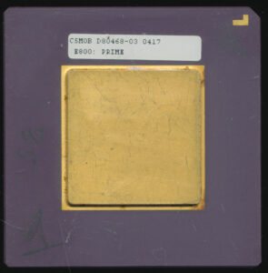
C5M – Ezra-T Prototype Pathfinder – PGA370
Most are familiar with the history of VIA so we won’t dive extensively into that but a quick summary is in order. VIA was founded in California in 1987 before moving to Taiwan, and previous to 1999 was well known for making chipsets and other support chips for computers. In 1999 VIA bought both Cyrix (from National Semiconductor) and Centaur Technologies (from IDT, who made the Winchip series of processors.
These purchases did two main things for VIA, it first gave them access to the x86 architecture, and it gave them legal leverage to continue down the x86 road. Cyrix possessed a license to the P6 processor bus (through a cross licensing with Intel) that was good until 2006. This allowed VIA to make what became the Centaur based CyrixIII/C3 processor on the P6 based Socket 370 platform. These are the processors and socket we are most familiar with for VIA CPUs. With clock speeds of 466-1.2GHz and eventual support for the Tualatin based boards these chips were the most ‘public’ facing CPUs. VIA also of course made many BGA versions, used in ITX form factor, and other mini type systems.
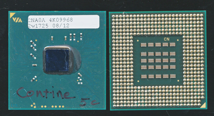
CNA – Isaiah – Interestingly using the old Pentium III-M pin out
The VIA designs, despite originally being called ‘CyrixIII’ were all based on the Centaur designed core. Intel, as was its custom, sued VIA in 2001 asserting patent infringement, which it is likely VIA was expecting. As with the case of Intel and Cyrix, VIA countersued, asserting Intel was infringing on patents VIA had acquired with the Centaur deal. In 2003 a settlement was reached that included a 10 year patent cross license between Intel and VIA and allowed VIA to continue to make x86 compatible processors (extended in 2013 by 5 years until 2018(. The deal also granted VIA a 4 year (with an extra optional year) license to continue to make chipsets compatible with Intel processors (they had originally signed a deal in 1998 to allow VIA to do so. This is how we continued to get VIA chipset based motherboards for Intel processors. The deal also added a small detail that leads to todays discussion, it granted VIA a 3 year grace period to continue making bus and pin compatible processors up through 2006.
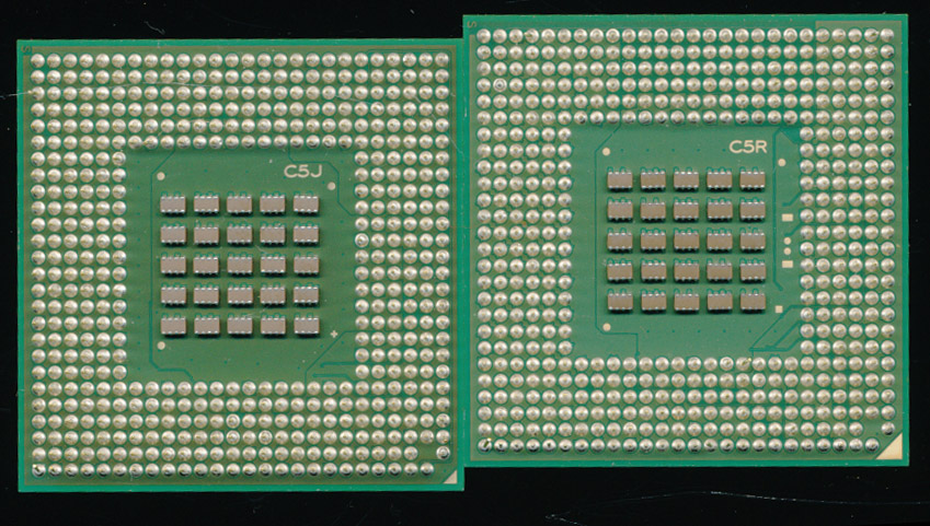
C5J (Left) and C5R (Right) – Banias Compatible Pentium M pin out
This last part is interesting, the fact that it was a grace period means it reflected what VIA was currently doing, not what they were planning to do in the future. The obvious example here is the C3 line on Socket 370 using the P6/Tualatin bus, but that was pretty old news in 2003 so what was VIA working on? CPU’s on more modern sockets of course, namely Socket 479 (mPGA479M) used by the Pentium-III-M (Tualatin) and Pentium M (Banias/Dothan). These use the same physical socket on a motherboard, but the keying pins are different on the CPUs themselves. These are all mobile designs which lend themselves well to VIAs low power designs. VIA did also make several reference boards for these CPU’s so its clear that there was plans for releasing them to the broader market, and likely with additional motherboard support.
C5J (Left) and C5R (Right) – C5R is a 110nm part with a slightly larger die the the C5J
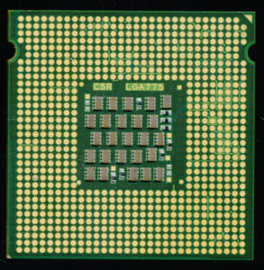
Another socket was just being developed at the time of this agreement, and that is perhaps the most interesting. Intel LGA775 chips began sampling in late 2003, which is after the grace period of 3 years had begun so it would make sense for VIA to not develop CPU’s using a socket they were going to lose access to in a few years. The package likely was in development for a couple years prior which is likely why VIA made a few (likely VERY few) samples for it. The samples are marked C5R which is a C7 Esther core, if VIA’s naming is consistent, this would be the TSMC 110nm version of the 90nm C5J.
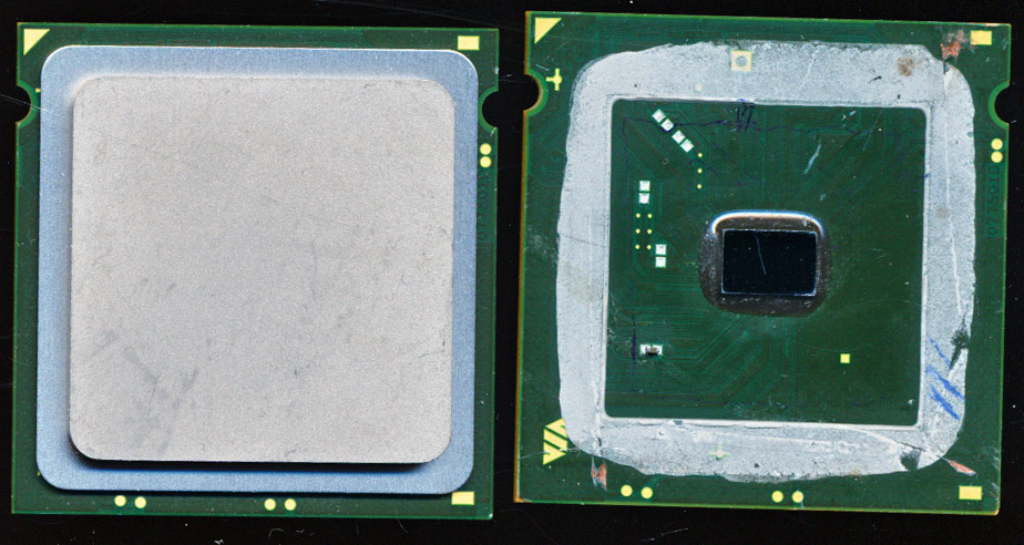
C5R With heatspreader and with heatspreader removed.
The Esther core code names are a bit confusing because of how some CPUID programs identify them. X-86-guide.net has a quite nice ID guide that goes into some great detail on them. In summary there was a 90nm Rev A C5J made by IBM, and later a 90nm C5J (called Rev D) made by Fujitsu with some additional features. This Rev D part often gets identified as a C5R, or a C5J shrink, neither of which is correct. The actual C5R (and related C5Q) were what appear to be backup plans for the IBM produced parts, using a larger 130/110nm process at TSMC. Looking at the mPGA479 unfinished packages (labeled C5J and C5R) the die attach area on the C5R is actually slightly LARGER then the C5J (~35mm2 compared to 28mm2 of the C5J)
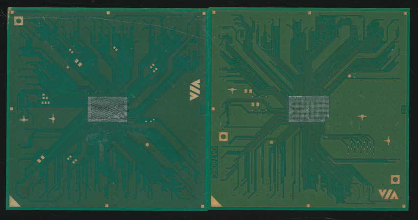
C5R Esther – 110nm TSMC in LGA775
Most VIA samples are labeled with the code name in Cxx format and not the marketing code name (Esther Isaiah etc) as each of the Marketing code names (for lack of a better term) consisted of many actual sub-cores.
| Code | Code Name | Process | Die Size (sq. mm) |
Notes |
| C5A | Samuel | TSMC 180nm | 75 | |
| C5B | Samuel 2 | TSMC 150nm | 52 | |
| C5C | Ezra | TSMC 150/130nm | 52 | |
| C5M | Ezra-T | TSMC 130nm | Proto Only (Pathfinder) | |
| C5N | Ezra-T | TSMC 130nm | 56 | Cu Interconnects – Low-k – Tualatin Bus |
| C5X | Nehemiah | TSMC 130nm | 78 | 10% Faster then C5XL – Higher power |
| C5XL | Nehemiah | TSMC 130nm | 52 | 133FSB |
| C5XP | Nehemiah | Low Power C5XL – Not released | ||
| C5P | Nehemiah | TSMC 130nm | 47 | 200FSB – DP Support |
| C5Y | Nehemiah | Unreleased – Adds SSE2 | ||
| C5Z | Nehemiah | Unreleased – VIA V4 System Bus | ||
| C5I | Esther | 90nm | Initial Esther – Almost Taped out | |
| C5J | Esther | Rev A 90nm IBM Rev D 90nm Fujitsu |
||
| C5Q | Esther | TSMC 130nm | Unreleased | |
| C5R | Esther | TSMC 110nm | Unreleased – Samples Made | |
| C5W | Esther | IBM 90nm SOI | Canceled early | |
| CNA | Isaiah | Fujitsu 65nm | VIA Nano 1000/2000 | |
| CNB | Isaiah | Fujitsu 65nm | VIA Nano 3000 | |
| CNQ | Isaiah | TSMC 40nm | VIA Nano X2 4000 VIA Eden X2 4000, VIA QuadCore E U4000 / L4000 – (two die VIA Nano X2 or VIA Eden X2) | |
| CNR | Isaiah | TSMC 28nm | VIA QuadCore E – C4000, VIA Eden X4 C4000 | |
Looking at the table above we can see VIA took many roads in the development of their CPUs, with many that went nowhere. Some may see this as a lack of direction or focus, but in a lot of ways VIA seemed to be trying to figure out the best CPU for the market at the same time they were trying to make the best CPU from an engineering standpoint. Where these two paths converged you had a marketable CPU that made it into mass production, and where they didn’t, or where legal road blocks arose, the design was canceled. VIA’s CPU development is even more obscure now, though they have made a few other designs we will cover in a later article, as well as the return of Intel to the VIA party.
February 6th, 2022 at 11:49 am
We are buying all types of electronic e-waste Scrap cards and other all types of e wast scrap for recycling +91 8910469826