Archive for the 'Processor Manufacturers' Category

September 29th, 2022 ~ by admin

Socialist Romania Computer Chips

The socialist bloc of countries that arose after World War II was not a monolithic entity, it had significant country and cultural differences. A number of countries stood apart, one of them was socialist Romania. The leadership of Romania pursued a relatively free domestic and foreign policy, while remaining within the framework of the socialist system and being a strategic ally of the USSR and a member of the Warsaw Pact.

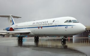
Rombac 1-11 – National Treasure of Romania

Through the CMEA (Council for Mutual Economic Assistance), the USSR assigned Romania the role of a supplier of agricultural products. The “big brother” proposed to mothball the agrarian backwardness of the republic, which did not suit Bucharest at all. In the late 60s, Romania chose to stand on the path of intensive industrialization. Hydroelectric dams block the Carpathian rivers, and then the Danube. Light industry plants work at their maximum capacity – thus, the country becomes the largest exporter of textiles in Europe. Enterprises of ferrous and non-ferrous metallurgy, chemical and petrochemical, and furniture industries were built. The extraction of precious and non-ferrous metals, uranium, oil, gas, coal were developed intensively. Since the early 1970s, Romanian enterprises have been producing large numbers of machine tools, turbines for power plants, cars, locomotives, tractors, combines, trucks, and household appliances. In the summer of 1979, Romania bought a license from British BAE Systems to produce the BAC 1-11 passenger jet. It was produced at the purpose-built Romaero plant in Bucharest. In total, under Ceausescu, 9 Rombac 1-11 planes were built.

At the beginning of the 1980’s, there were two entities in Romania that produced electronic components, IPRS and ICCE

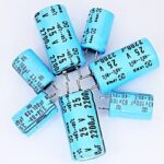
IPRS-Băneasa, Bucharest. By the early 1980s, the company had over 6,000 employees and nine production facilities. It was located on 15 hectares (37 acres) of land on the edge of the Băneasa forest near Bucharest. Products (capacitors‎, diodes, analog and digital ICs, thyristors, transistors) were sent not only to the countries of the socialist bloc, but also to Asia and Western Europe.


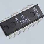
ICCE  (Research Institute of Electronic Components) was built outside the premises of IPRS-Băneasa, but in close proximity. In 1979, the micro-production department of the institute was opened. From that moment on, ICCE was able to supply many of the components developed at the institute, namely those that were requested in relatively small quantities (thousands per month) and which IPRS-Băneasa did not produce because it was not economically viable. Thus, it can be said that ICCE was not a real competitor for IPRS-Băneasa, but rather an addition. For example, in the 1980s, so-called special programs appeared, required electronic components for the Oltcit plant, for the heavy water plant in Turnu Severin, for the nuclear power plant in Cernavodă, as well as for the army. These components were needed in relatively small quantities, with harsh operating conditions carefully selected through reliability programs.

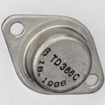
But a third entity that appeared later is of much interest to us, Microelectronica (ME) was set up in 1981 close to I.P.R.S. and ICCE with the goal of manufacturing PMOS, NMOS, and CMOS integrated circuits as well as optoelectronics, complementing the production profile of I.P.R.S. At its inception, ME had about 40-50 employees, most of them engineers, representing the Microelectronics group at ICCE.

Read More »

October 12th, 2018 ~ by admin

Xilinx gets ARMed up for Free

Xilinx Virtex II Pro FPGAs from the 2000’s included embedded PowerPC processor cores.

Recently ARM announced they would be providing IP for the Cortex-M1 and M3 cores for free for users of Xilinx FPGA’s.  The Cortex-M1 and M3 are some of the most basic ARM cores, taking 12-25,000 gates for the Von Neumann architecture M1 and around 43,000 for the full up Harvard architecture M3 (with full ARM THUMB instruction set support).  Xilinx already offers FPGAs/SoCs with built in ARM cores, the SYNQ series is available with a variety of high end ARM cores such as the Cortex-A53 and the RF focused R5 core.  These obviously are fairly high gate county, and cost cores, where as the M1 and M3 cores are being provided without license, and without any royalties.  Drop in the IP into your FPGA design and go.

ARM and Xilinx say this is to meet the needs of their customers, who want to be able to use the same ARM architecture in their FPGA designs as in ASICs etc, and at the lowest investment in time and cost.  This certainly makes sense, having a free ARM core is better then a low cost ARM core, and removing the ‘paperwork’ hassle helps, but that’s probably not the only reason ARM is doing this, and doing it specifically for Xilinx.

There are a couple other things at play here, ARM Mx cores are basic RISC processors, used for when you just need to get some basic processing done, no frills, low power, and easy to use.  It turns out that’s a market that is now seeing some competition from the SiFive RISC-V core.  This is a basic, easy to use RISC core, that is synthesizable into ASICS, and FPGAs, and comes with a one time low cost license fee and no royalties.  Its being used by such heavyweights as Nvidia, and could threaten the Cortex-Mx domain, so it makes sense for ARM to offer, essentially their introductory processor core, for free, as a way to sway people to the ARM ecosystem.  But why Xilinx?

Perhaps Xilinx is just the start of ARM’s plans, Xilinx is one of the biggest providers of FPGAs in the world so certainly that will help keep people in the ARM. Xilinx infact, already has a drop-in 32-bit RISC processor core available to all their customers, the MicroBlaze and PicoBlaze, of their own design.  There are also drop in 80C186 cores, MCS-51 cores, the LEON SPARC core and many others. The other big name in FPGAs is Altera, a company that has competed with Xilinx for the better part of 30-years and was, in June of 2015 bought by none other then Intel.

Altera has had a close relationship with Intel since the 1980’s when Intel first started assisting Altera with fab’ing their PLDs.

This gave Altera greater access to Intel’s fab/engineering prowess, but also to all of Intel’s IP.  Is Intel going to offer free ARM cores on Altera FPGAs (the Stratix/Arria series does include hard Cortex-A9/A53 cores already)?  It seems unlikely that they would work to support their architectural competitor any more then they have to.  It is more likely that Intel would offer some form of 32-bit x86 processor core for their FPGAs.  Now x86 isn’t exactly known for low gate counts, but it is possible.  Currently softcore 8086 and 80186 processor (the Turbo86 and Turbo186) are 22,000 and 30,000 gates respectively, really a rounding error in FPGAs that now have millions of gates. More and more, FPGAs are becoming less FPGA like, and more ‘configurable processor’ like.

July 11th, 2016 ~ by admin

Sparkplugs, O-Scopes and Cell Phones…

AMD 486 processor. Note the logo in the lower right corner. Package is from Kyocera (Click for larger version)

AMD 486 processor. Note the logo in the lower right corner. Package is from Kyocera (Click for larger version)

What do all 3 of these things have in common? And what in the world do they have to do with computer processors (ok modern oscilloscopes and cell phones DO have CPUs in them but spark plugs?). Tektronix was started here in Oregon in 1946 making oscilloscopes and other test equipment.  Throughout the last 70 years they have continued to do so, but along the way they also began to make everything needed to manufacture the final equipment they sold.  Design/simulation software, PCB manufacturing, IC manufacturing, displays, and even the packaging used for IC’s.  In recent years many of these vertically integrated operations have been spun off, but they do still maintain some.

Tektronix packaging options from the early 1990's (Click for larger version)

Tektronix packaging options from the early 1990’s (Click for larger version)


When an IC manufacturer (such as Intel, AMD, etc) designs/builds an IC what they typically are creating (or having made in the case of fabless companies) is the silicon die itself.  This little piece of silicon contains the millions of transistors needed to perform whatever task its made for, but for most uses that silicon die needs to be packaged to be useful.  A sliver of silicon is hard to work with and integrate into designs, a package provides the routing of wire/leads to the die, as well as protects it from the environment, while dissipating any heat it generates.

IC manufactures do not typically make their own packages, they are either contracted out or bought off the shelf.  Tektronix is one of several companies that makes and sells IC packages.  The pictured display is a sample of some of the packaging types they offered.  You can recognize some of the more common packages, as well as some more specialty ones such as the ‘POWER TAB’ that was used in analog equipment frequently (like audio amplifiers etc).

Anam/Amkor Test package

Anam/Amkor Test package

Tektronix isn’t the only company that offers packages for IC.  Perhaps the two largest are NGK and Kyocera.  Both have extensive experience with ceramics, a material very useful in IC packages.  Developing high strength, high temperature ceramics for spark plugs, isn’t so much different from designing the same for a high end processor.  Kyocera started life making ceramic insulators, well before ever getting into cell phones (in 2000) and ceramic packaging continues to be their core business.

Often times assembly and test of a IC is handled by yet another company.  Many companies (such as Amkor) entire business is based on taking IC dies from one company, assembling them into packages from another, testing them, and shipping them.  So next time you look at a CPU and read its makers name boldly written on its top, there is a good chance that that name had but one part in that IC.

January 21st, 2016 ~ by admin

Microchip PIC’s up Atmel

Microchip PIC16C62 ENG SAMPLE - 1989

Microchip PIC16C62 ENG SAMPLE – 1989

Yesterday Microchip, makers of the PIC line of microcontrollers, announced they were buying Atmel, for a cool $3.56 Billion.  This isn’t entirely surprising considering the ongoing consolidation in the industry, It was only last year that Dialog attempted to purchase Atmel, and before that ON Semiconductor and Microchip. In December of 2015 NXP and Freescale (formerly Motorola Semiconductors) merged, creating one of the largest microelectronics companies.  These mergers do create an interesting result, product mixes that were formerly competitors, end up being marketed side by side.  In the case of NXP and Freescale, NXP marketed many MCS-51 microcontrollers in their 8/16-bit lines, while Freescale of course sold many versions of MC6800 based MCU’s.  These two rivalries have existed since the early 1980’s and likely will continue.  Perhaps the biggest rivalry in MCU though is between Atmel and Microchip.

Atmel EPROM, fab'd by GI in 1986, right before they became Microchip

Atmel EPROM, fab’d by GI in 1986, right before they became Microchip

Microchip was spun off of General Instrument in 1987, but the PIC architecture dates back to 1976, and is still being made in nearly the same form (PIC16C55).  Atmel was started in 1984, first making EPROMs, and then MCS-51 microcontrollers, one of the very first companies to make an 8051 with on die flash memory.  In a bit of a twist of fate, when Atmel started, it was a fabless company, it contracted with several companies to make its EPROMs, including Sanyo, and General Instruments, which as mentioned above, became Microchip.  Atmel also makes APRC processors, and for a time made Motorola products as well (Atmel has a very convoluted history, for more info on this read here and here )

Today the PIC line continues to be popular, with devices for the low end, such as the PIC10/12 all the way to the MIPS based PIC24 on the upper end.  Atmel continues to make 8051 MCUs, but also makes the 8 and 32-bit AVR line, perhaps best known today for its use in Arduino boards.  They also make MCU’s based on the ARM core, a competitor to MIPS, and Atmel’s own AVR32.

Likely to the consternation to many fans of either company, this merger does make sense, more so than ON or Dialog buying Atmel.  While Microchip and Atmel both compete in the same markets, they do so with different architectures.  Product lines are unlikely to change, and overhead saving should free up $$ both for stockholders (yawn) and engineering teams alike. No word has been giving yet on wether Microchip intends to keep the Atmel branding, but perhaps they should, as an AVR MCU with a Microchip logo on it may just prove to be too much for some.

January 18th, 2015 ~ by admin

Hua Ko HKE65SC02PL – GTE Micros Asian Twin

Hua Ko CMOS 6502 - 4Mhz Industrial Temp - Direct copy from GTE Micro

Hua Ko CMOS 6502 – 4Mhz Industrial Temp – Direct copy from GTE Micro

Hua Ko Electronics was started in 1979 in Hong Kong, though with close ties to the PRC. Their story is a bit more interesting then their products, which were largely second sources of western designs. In 1980 they started a subsidiary in San Jose, CA. This was a design services center mainly ran as a foundry for other companies. They developed mask sets in their CA facility but wafer fab and most assembly was done back in Hong Kong (as well as the Philippines by 1984). Chipex also had a side business, they were illegally copying clients designs and sending them back to the PRC. In addition they were sending proprietary (and restricted) equipment back to Hong Kong and the PRC. in 1982 their San Jose facilities were raided and equipment seized. Several employees were arrested and later charged and convicted. The following investigation showed that the PRC consulate had provided support and guidance for Chipex’s operations and illegal activities. So where exactly did the HKE65SC02 design come from?

Read More »

May 9th, 2011 ~ by admin

Intel’s Ivy Bridge: 50 Years of flat transistors come to an end

Traditional microprocessor transistors are "planar" or flat as they pass through the switching gate

April marked the 50th anniversary of Robert Noyce’s patent on making silicon IC’s with a planar process, a concept that has changed little since then.  That is, until this month, when Intel announced their new 22nm process, a process that will not be restricted to planar transistors.  Intel, like Hollywood as of late, has gone 3D, Instead of a transistor being built in planes (layers) Intel has developed a way to produce transistors with source/drain spanning several planes on the die, essentially they are formed vertically, rather then horizontally.

This in an of itself is not remarkable, it has been thought of, and done before. What Intel did is make it happen on a commercially viable process.  Intel claims to be able to initially manufacture these on a commercial scale at only a 3% cost increase over traditional planar processes, and of course expects that 3% added cost to drop to zero, or in fact result in a cost savings, as the process is refined.

The Tri-Gate system features 3D "fins". This allows the same surface area, in a smaller die area.

What this allows is 2-3 times the number of transistors in the same space as a planar process (assuming the same process size).  Intel plans to use this process for the 22nm node. Intel’s first processor, the 4004, was constructed on a 10 micron process with 2300 transistors.  Thats 500,000 times larger features and over a million times less transistors, yet it consumed almost a 1 watt of power.  With Intel’s new 3-D 22nm process it should give Intel the break they need into the mobile phone market, a market they have been desiring to reenter ever since selling off their mobile ARM (PXA//StrongARM) division to Marvell several years ago.

February 5th, 2011 ~ by admin

Atmel Buys MHS, Again – The Twisted History of Atmel, Temic and MHS

Today Atmel purchased MHS Electronics, a French company.  Why is this interesting? Because this is not the first time Atmel has bought MHS, in one form or another.  Atmel, Matra, MHS, and Temic’s histories are rather intertwined, with mergers, acquisitions and name changes occurring frequently over the last 25 years.

A Bit of History….

Atmel 4Mbit EPROM - 1995

Atmel was founded in 1984 by George Perlegos, a former Intel employee, as a fab-less semiconductor company.  Originally Atmel designed EPROM’s and PLDs.  They were manufactured by Sanyo, which had an Intel license.  Intel, however, sued Atmel (along with Hyundai, iCT, AAS, Cypress, and Pacesetter Electronics) over EPROM patents in 1987.  The courts sided with Intel which severely hampered Atmel’s ability to make EPROM’s.  Their focus then switched to non-volatile memories, such as Flash for which they have become very well known and continue to make.  In 1989 they bought their own fab (from Honeywell) in Colorado Springs, CO and in 1993 released an 8051 (Intel licensed) with integrated Flash memory.  This catapulted Atmel into the microcontroller market that is today one of their core businesses.  In 1994 Atmel Purchased SEEQ, an EPROM and EEPROM company that Perlegos helped start in 1981.  In 1995 Atmel opened a fab in Rousset, France, thus beginning the French connection.

Temic 80C32 - 1998

Temic had its beginning in 1903 as Telefunken (Ironically a joint venture of Siemens and another company).  In 1967 AEG merged with Telefunken and in 1985 Daimler-Benz bought Telefunken-AEG and renamed it to simply AEG. The semiconductor division of AEG was then called TEMIC (TElefunken MICroelectronics).  In 1998 AEG sold TEMIC to Vishay, another automotive electronics supplier.  Vishay only had interest in the discrete and power electronics portions so immediately sold the IC portion to Atmel. This gave Atmel a Bipolar fab in Germany

Matra Harris Semiconductors SA (MHS) was created in 1979 as a joint venture between Matra, the French high technology group, and Harris Semiconductor, an American semiconductor manufacturer. In 1989, Harris withdrew from the partnership, and the name was changed to Matra MHS SA. Two years later, AEG (The electronics division of Daimler-Benz) purchased 50% of Matra and merged the unit with its TEMIC Semiconductor subsidiary. In 1998, AEG purchased the remaining shares of the company and the name was changed again, to MHS SA.

MHS 80C52 - 1988

This was part of the sale to Vishay mentioned above, which Atmel then purchased.  MHS had one CMOS fab in Nantes, France which was included in the sale

Here is where it gets complicated…

The result of all of this was Atmel now owned Temic, MHS, 2 fabs in France, one in Germany, their original fab in Colorado as well as a fab in England, and one in Texas.  Atmel needed to consolidate their fabs so in 2005 they sold the MHS fab in Nantes France to Xbybus, a French company. Xbybus ran the Nantes fab as MHS Electronics.  In 2008 Atmel sold their fab in Germany (the former TEMIC fab) to Tejas semiconductor.  This left Atmel with one fab in Colorado, and one in Rousset, France.  Labor issues at the French fab in regards to Atmel’s need to reduce production led to indefinite strikes at this fab, hampering Atmel’s work to sell it.  Finally in 2010 Atmel received approval from the French gov’t to sell the fab to LFoundry, a French company.  This marked the end of Atmel’s fab presence in France…..

Telefunken U3870M CPU (Mostek Clone) - 1986

For about 9 months…

Today, Atmel has bought MHS Electronics, and their fab in Nantes, France, a fab they owned from 1998-2005.  MHS had been having financial troubles since 2008.  An interesting end to a series of event that began over 30 years ago.

I suspect though that we have not yet heard the last of MHS, or perhaps TEMIC.

February 1st, 2011 ~ by admin

Shrinking Process size Shrinking Foundry Selection

The processes used in manufacturing processors has been shrinking ever since the IC was invented.  In the 1970’s the common feature size was 10 microns.  Today many chips are made on a 22nm (0.022micron) process.  The cost of equipment to manufacture IC’s on such a small process has been increasing rapidly.  The cost of equipment goes up much higher then the the rate of process shrink.  Put another way, to half the process technology, equipments costs are significantly higher then merely double.

What this is causing is something that has happened, or is happening in most other mature industries.  Initially the technology is equally expensive, and accessible to each company, so many companies make the dive into it.  As the technoogy becomes more expensive, it becomes more exclusive.  A company must have the revenues (by having a very succesful product line) to afford the capital expenditures to move to the next technology.

This results in consolidation, many companies do not have the revenues to afford to upgrade their fabs; some companies start out knowing this and operate as a fab-less company, relying solely on contract foundries to make their parts.  In the 1970’s and even the 1980’s this was the exception.  Today, it is the rule.  IC companies simply cannot afford to keep a fab running at the latest tech level.

2011 Foundries by process technology

19 different foundries have 130nm capabilities, a process that was introduced in 2000.  This is a fine process for many applications but certainly not very useful for most low-power (such as mobile) applications.  At a 32mn process the number of foundries has dropped to only 6 with only 4 of those expected to hit 22nm this year.  TSMC is a pure play foundry, they make no products of their own, solely parts for other companies.  Globalfoundries is the foundry spinoff of AMD, and now operates much like TSMC.  Samsung does both, they make many products themselves (The Apple A4 processor being one of the better known products) as well as provide foundry services for other companies.  Intel recently started to experiment with working as a foundry, perhaps to take up any slack they may have in their fabs.  One particularly interesting note is that Japanese fabs have not been able, or willing to keep up with technology.  This may have to do with how fragmented that market was, and may change as more Japanese IC companies consolidate (such as Mitsubishi, Hitachi and NEC forming Renesas).

This trend will continue as technology advances and becomes more expensive to produce.  However, many products simply do not need to be made on the most advanced process. Your toaster oven is just fine with running ICs made on a 130nm process, and thats unlikely to change.  As long as there are 3-4 foundries on the leading edge, competition will keep driving advances in technology, and reductions in costs.

April 22nd, 2010 ~ by admin

Apple rumored to buy ARM Holdings

AppleInsider has a post up about a potential interest Apple has in ARM Holdings, designers of the ARM processor cores used in the iPod, iPhone, and iPad, among tens of thousands of other devices. Apple has a market cap, of almost $250 billion, while ARM is just shy of $2 billion. Apple clearly has the cash abilty to purchase ARM outright, and they certainly have a reason to want to.

However, the rest of the computer world has an even bigger reason to keep Apple from doing so.  ARM devices are used by tens of thousands of devices, made by thousands of companies. Silicon containing ARM IP is made by hundreds of companies across the world. The success of these companies, their designs, and the devices they power is in large part based on fair, equal, and predictable availability of licenses from ARM.

If Apple were to own ARM, they could completely stop the availability of licenses to any design they felt was a competitor, or they could delay the release to third parties of newer designs. This is similar to the problem some phone companies are experiencing with Google and their Android OS, Google is motivated to sell their own branded Nexus One phone, with the latest version of Android, before giving the same version to third parties.

Read More »

April 5th, 2010 ~ by admin

Apple iPad Round up: Inside and Out The Processors of Apple’s Latest

Apple Officially has launched the iPad, essentially a scaled up iPhone, and judging by the model number, it started development several years ago around the time of the first iPod Touch. Many of the components are similar to the iPhone, if not the same. Obviously the biggest processor ews is the Apple A4 ARM processor at its heart. Its developed by Apple, and built by Samsung. a multi-die package, it includes the ARM processor, and PowerVR Graphics on one die, and then two 128MB DRAM dies as well.

iPad Motherboard - A4 CPU by Samsung

What is interesting about the A4? It has a 64bit memory bus, rather then the more standard 32bit but found on most ARM devices. This likely for faster memory access to support faster graphics.

Wifi, Bluetooth, and FM functions are handled by a Broadcom BCM4329 which includes two processors of its own (the documentation of this part does not state what architecture they are, but MIPS or XA-RISC is likely)

The screen controller is the Broadcom BCM5973/5974 which has been used by Apple for several years. The Baseband processor in the 3G version is the Infineon X-Gold 608 which contains a 312MHz ARM926 processor, a 2007 design, so probably saved Apple some money.

So all told the iPad 3G contains at least 4 seperate processors.

Instrinsity: ARM Processor Design House

In related news rumors are flying about Apple acquiring Intrinsity. Instrinsity is a processor design house which specializes in, you guessed it, ARM processors. Its likely they have helped Apple more on the A4 then P.A. Semi (another Apple acquisition) This is further supported by the fact that Intrinsity has worked a lot lately with Samsung in developing a 1GHz ARM CPU (the Hummingbird). Who fab’s the A4? Yah, Samsung.

Sources:
EE Times: Inside the iPad
EE TImes: Inside the iPad: Broadcom/Samsung
iFixit: Teardown
ars technica: Apple buys Instrinsity