November 15th, 2014 ~ by admin
Anandtech has an excellent article on the new Apple A8X processor that powers the iPad Air 2. This is an interesting processor for Apple, but perhaps more interesting is its use, and the reasoning for it. Like the A5X and A6X before it (there was no A7X) it is an upgrade/enhancement from the A8 it is based on. In the A5X the CPU was moved from a single core to a dual core and the GPU was increased from a dual core PowerVR SGX543MP2 to a quad-core PowerVR SGX543MP4. The A6X kept the same dual core CPU design as the A6 but went from a tri-core SGX543MP3 to a quad core SGX554MP4. Clock speeds were increased in the A5X and A6X over the A5 and A6 respectively.
The A8X continues on this track. The A8X adds a third CPU core, and doubles the GX6450 GPU cores to 8. This is interesting as Imagination Technologies (whom the GPUs are licensed from) doesn’t officially support or provide an octa-core GPU. Apple;s license with Imagination clearly allows customization though. This is similar to the ARM Architecture license that they have. They are not restricted to off the shelf ARM, or Imagination cores, they have free reign to design/customize the CPU and GPU cores. This type of licensing is more expensive, but it allows much greater flexibility.
This brings us to the why. The A8X is the processor the the newly released iPad Air 2, the previous iPad air ran an A7, which wasn’t a particularly bad processor. The iPad Air 2 has basically the same spec’s as the previous model, importantly the screen resolution is the same and no significantly processor intense features were added.
When Apple moved from the iPad 2 to the iPad (third gen) they doubled the pixel density, so it made sense for the A5X to have additional CPU and GPU cores to handle the significantly increased amount of processing for that screen. Moving from the A7 to the A8 in the iPad Air 2 would make clear sense from a battery life point of view as well, the new Air has a much smaller batter so battery life must be enhanced, which is something Apple worked very hard on with the A8. Moving to the A8X, as well as doubling the RAM though doesn’t tell us that Apple was only concerned about battery life (though surely the A8X can turn on/off cores as needed). Apple clearly felt that the iPad needed a significant performance boost as well, and by all reports the Air 2 is stunningly fast.
It does beg the question though? What else may Apple have in store for such a powerful SoC?
November 3rd, 2014 ~ by admin
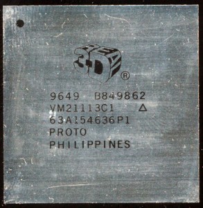
Real3D VM21113C1 Prototype (likely a Pro/1000)
Much of consumer tech starts life in the labs of defense companies. The reasons of course are simple, defense projects demand high tech, and are paid high prices by their respective governments. Usually this tech is eventually spun off or licensed to consumer companies. Occasionally, however, a defense company will commercialize a product on their own. Thus was the case of Real3D.
Real3D has its roots in GE Aerospace. GE needed to make simulators, with graphics good enough to be useful for training for a variety of systems. Their first system was a docking simulator for the Apollo Project in the 1960’s. By the 1980’s the technology had evolved into graphics systems for other simulators, notably the M1 Tank. This simulator used texture mapping graphics, which was in the world of sprites commonly used on PC’s was rather high tech. In 1992 GE sold the GE Aerospace division to Martin-Marietta who then merged with Lockheed. Lockheed Martin wanted to commercialize the graphics work GE Aerospace has developed and thus formed Real3D Inc. in 1995. Real3D’s first commercial success was the graphics work on the Sega Model 2 (Real3D/100) and 3 (Pro-1000) arcade systems. Real3D also began working with SGI and Intel on a PC based graphic solution to take advantage of the new AGP bus. This was known as the Starfighter, and later as the rather infamous Intel i740, its performance was not particularly good, but it was what Intel wanted for their entry into the value graphics market. Real3D also had the Pro-1000 whose performance was much better but it never made it out of the development stage.
In 1999 Lockheed closed Real3D and sold its assets (mainly IP) to Intel. The i740 was withdrawn from the market in 1999 as well, but its technology, and that of Real3D continued to be used by Intel in their integrated graphics chipsets (notably the i810 and i815), surviving still to this day. While no competitor to AMD/Nvidia Graphics it still is enough for most computing.
December 3rd, 2012 ~ by admin

SGI Extreme 4GE7MCM 256 MFLOPS 320,000 Gates
At 2.6oz (75 grams) and 2.25 inches square (6cm) the SGI 4GE7MCM is a beast of a graphics chip. More properly called a Geometry Engine was, the GE7 was responsible for all the graphics processing in SGI Indigo2 workstations. The Indigo2 Extreme graphics option consisted of a pair of these MCMs (Multi-Chip-Module). Each one contains 4 GE7 Geometry Engines providing 32MFLOPS of performance each. Each GE7 consists of a custom 80,000 gate array from LSI (for a total of 320,000 gates and 128MFLOPS per MCM). This performance level was, ironically, better then the main system CPU (35MFLOPs for the 200MHz R4400 option).
Each of the black ‘caps’ on the chip covers a single GE7 Engine. A similar design was used for the XZ Graphics system that had only 4 total GE7 cores. This was either implemented with 2 of the large MCMs that had only 2 GE7s in them (same package however) that were marked 2GE7MCM, or, later, a single surface mount MCM containing 4 GE7 engines. All were manufactured by LSI. In total the Extreme Graphics subsystem had no less then 31 custom gate arrays from LSI for a total of over 1.2 million gates. At an average of 2 transistors per gate that works out to around 2.5 million transistors, a considerable amount for a graphics system in 1993. Today’s graphics chips pack in transistors numbering in the billions, the Geforce GTX 680 has a total of 3.54 billion transistors, and performance measured in TFLOPS, again for the GTX 680, 3.09TFLOPS. Today’s graphics chips cannot, however, compete with the magnificent looks of the GE7’s giant MCM package.
Sources:
Indigo2 Product Guide (PDF)
Indigo2 Technical Report
July 28th, 2012 ~ by admin
While we don’t actively collect GPU’s, we do pick them up when they come along, rather then scrap them, and from time to time have been donated a handful of them. Here are a few that have been sitting on my desk that were donated. GPU’s are pretty impressive in their own right (with many having over 1 billion transistors now)

Nvidia NV43 ENG SAMPLE
The NV43 is the code name for the Geforce 6600. It was released in August 2004 (abut the time this Engineering Sample was made) and could be clocked at up to 525MHz. It was fab’d by TSMC on a 110nm process and contains 143 million transistors (about the same as a Pentium-M Dothan core).
Read More »


