April 16th, 2020 ~ by admin

DEC M7260 KD11-A CPU: The PDP-11 Goes MSI

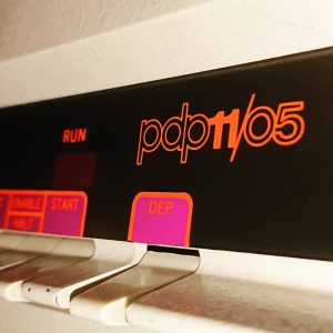
PDP-11/05 Front Panel (pic from vintage_electron)

Back in 1972 DEC released the ‘budget’ PDP-11/05 16-bit computer.  The original PDP-11/20 had been released 3 years before and its CPU (the KA11) was based on simple TTL, its ALU could perform adds and that was all, which meant its designers had to get creative in implementing the instruction set.  By 1972 however things had changed, there still was no 16-bit processors available but there was now single chip 4-bit ALU’s.  The ALU was the famous 74181 and formed the heart of the KD11-A, DEC’s 4th processor design (the ‘third’ was the KB11-A which was similar but based on the faster 74S181 and used in the PDP-11/45 and released at the same time) .

The KD11-A consisted of a pair of boards, the M7260 Data Path Module and the M7261 Control Logic and Microprogram Module.  All the processor functional components are contained on these modules. The M7260 Data Path Module contains: data path logic, processor status word logic, auxiliary arithmetic logic unit control, instruction register and decoding logic, and serial communications line interface. The M7261 Control Logic and Microprogram Module contains: internal address detecting logic, stack control logic, Unibus control logic, priority arbitration logic, Unibus drivers and receivers, microbranch logic, microprogram counter, control store logic, power fail logic, line clock, and processor clock.   The M7260 was he brain, and the M7261 told it what to do, containing the microcode to implement the PDP-11 instruction set.  This was the first version (with the 11/45) of the PDP-11 that was microcoded.

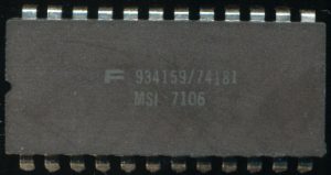
Fairchild 934159 74181 MSI 4-bit ALU made on a Bipolar – This example from very early 1971

The KD11-A ran off a single 150ns clock resulting in a raw clock speed of 6.67MHz, however performance was limited by memory access speed. The PDP-11/05 supported up to 32K Words (64KB) of core memory and this memory could only run at a 980ns cycle time.  This limited the 11/05 performance to around 1MHz.  This was still quite good for 1972!.

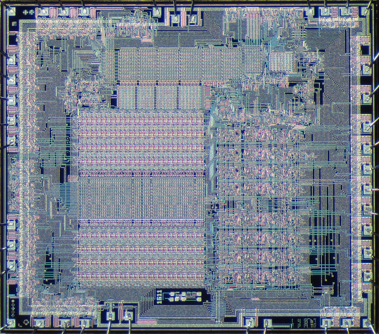
The 74181 was capable of running at 42MHz (and 90MHz for the 74S181 Schottky TTL versions) but in a set of 4 this drops to about 27MHz (with the carry generator taking some time).   Speed, however, is usually limited by other things rather then the ALU itself.   The 74181 ALU contains the equivalent of 62 logic gates (170 transistors) and can perform 16 different arithmetic and logic functions on a pair of 4-bit inputs.  Ken Shirriff did an excellent die level analysis of a ‘181 thats worth reading.  It includes pretty pictures even.

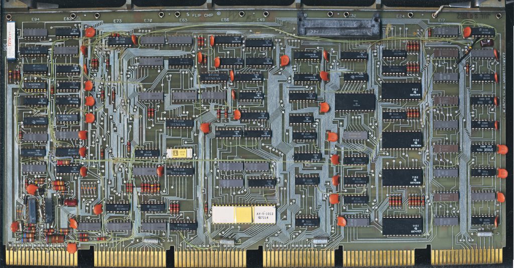
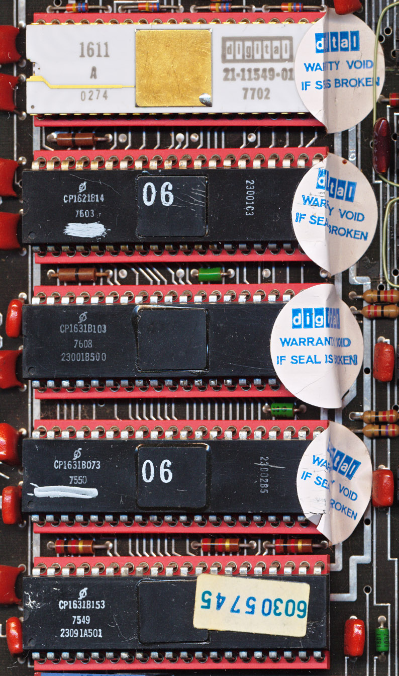
DEC M7260 – Data Path for the KD11-B CPU – Dated July 1972

This particular KD11-A board is one of the very first made.  It is dated July 20th 1972, a month after the initial release of the 11/05.  The big white chip is a General Instruments AY-5-1012 UART.  To its right you can see thr 4 74181 ALUs.  Each is 4-bit and together they form a complete 16-bit ALU for the CPU. A 74150 Multiplexer helps determine what data goes where.  The 74182 is the Look ahead carry generator for the ‘181’s.  Most of the rest of the chips on the board are ROMs and supporting logic.  There is also 4 Intel C3101A 35ns SRAM chips, these are 16×4 SRAMs used as scratch pad memories and only were used in the very first version of the CPU (later versions replaced them with cheaper 7489 TTL versions).  The Scratch Pad Memory is what forms the registers for the CPU.  There are 16 16-bit registers with the the first 6, R0-R5 being general purpose registers and the rest special purpose such as the Program Counter, Interrupt Vector, etc.

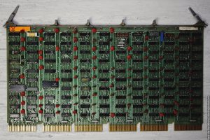
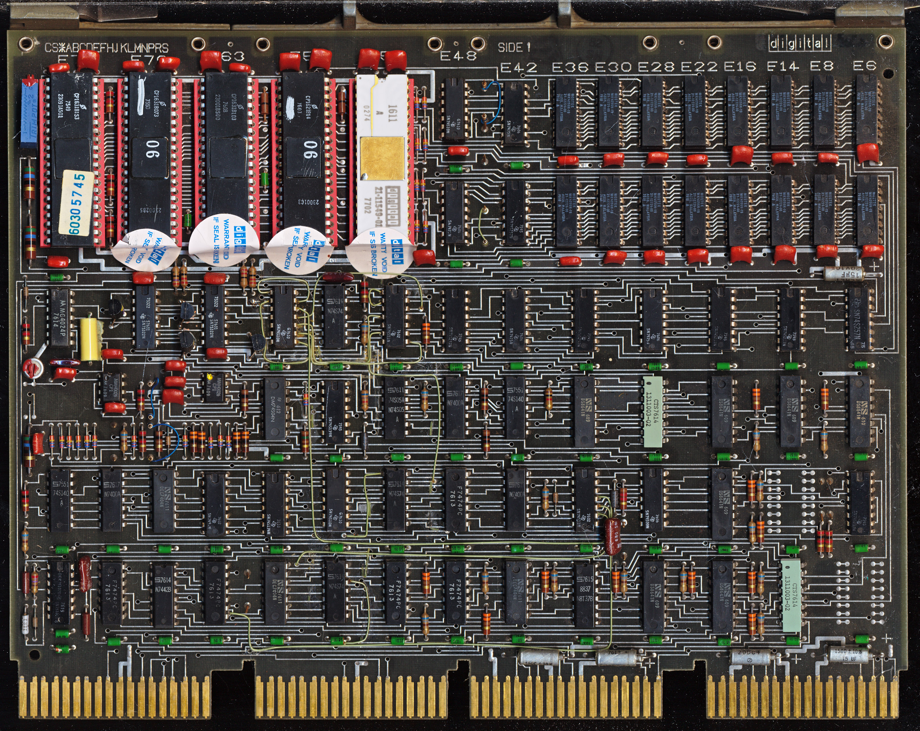
M7261 Control module – Contains the microcode for the CPU (pic from xlat.livejournal.com)

Another interesting point on this board is the very large amount of green wires running on the board.  These are called ECO wires, which are ‘Engineering Change Order’ wires, and are placed, by hand, after the board is made to correct faults in the board layout.  The goal is to not have these as they are expensive and delicate and can result in failures down the road, so further revisions of the board would have these fixed/implemented in the PCB.  You do not see these much at all any more as modern design/testing tools virtually eliminate the possibility of a faulty PCB layout making it into production.

When it was released the ~1MHz 11/05 cost $25,000, which in 2020 US Dollars is around $154,000.  THe PDP-11 series ended up being one of the most popular minicomputers, selling over 600,000 units over the years.  Later versions like the LSI-11 series moved the entire CPU to a single LSI chip, adding Extended Instructions, Floating Point Instructions, faster memories and other performance enhancements well into the 1980’s.   It was also widely comied, and enhanced in the Soviet Union and Russia.  It was on a Soviet PDP-11 clone that Tetris was developed, a game we are all rather familiar with.

Its amazing to see where computers have come in the span of but a few decades. but these important parts of history continue to be used.  Perhaps not the 11/05, but there are many PDP-11 systems still working away, typically inindustrial environments, ironically helping produce things likely far more advanced then themselves.

Posted in:
CPU of the Day

November 22nd, 2017 ~ by admin

CPU of the Day: DEC LSI-11 Chipset

LSI-11 Chipset with EIS/FIS Chip – 1976-1977

Back in 2014 we discussed the Western Digital WD/9000 Pascal Microcomputer system.  Today we’ll look at the LSI-11 chip set, the basis of the Pascal.  Back in 1974 DEC (Digital Equipment Corporation) contracted Western Digital to design and build a 16-bit chipset to emulate the Bipolar PDP-11/05 Minicomputer.  Western Digital was paid $6.3 million for the work, and would be allowed to market and sell the resulting chipset themselves, as well as grant license to it to others (including DEC).

The LSI-11 was to be a 16-bit chipset, but was based around a 8-bit Data chips (the 1611).  The 1611 has an 8-bit ALU , 26 8-bit registers and a microinstruction register.  This is controlled by the 1621 control chip, which interprets macroinstructions from handles all the timing, as well as interrupts.  The 1621 control chip is what allows the 8-bit 1611 to be used as a 16-bit processor.  The chips are connected by an 18-bit  microinstruction bus, and a 16-bit address/data bus handles access to the rest of the system (memory/I/O).  Each microm is a 512 Word by 22-bit ROM, which can hold 80 instructions.  It is these MICROMs that allow the WD MCP1600 to function as a PDP-11/05.  The instructions in the the MICROMs (2 are required for the LSI-11) emulate the PDP-11 instructions.

DEC M7264 LSI-11 KD11-L Board from PDP- 11/03

First production of the LSI-11 chipset began in March of 1975 with shipments commencing that year.  The PDP-11/03 based on this chipset was released later that year.  The KD-11 M7264 board formed the hear of the 11/03 (as well as other DEC systems).  In typical DEC fashion it came in many flavors with different amounts of memory, as well as different instruction support.  This was completely due to the design of the LSI-11 chipset and its MICROMs .  The basic LSI-11 needs 2 MICROMs to handle the basic PDP-11 instructions, the chipset however supported 4.  This means that more instructions could be added.  One of the most common and useful additions was the EIS/FIS (Extended Instruction Set/Floating Point Instruction Set) microm.  This added 8 more instructions including MUL, DIV, FADD, FSUB, FMUL, FDIV and 2 register shifts (ASH, ASHC).  Adding the EIS/FIS chip to a standard KD-11-F board turned it into a KD-11-L (like the one pictured).

Western Digital 1611 Die –
Pauli Rautakorpi

There were other MICROMs available as well.  This included a set of 2 for support of DIBOL (Digital Business Oriented Language), a DEC language similar to COBOL.  Since the DIBOL chipset needed 2 chips a system could support DIBOL, OR EIS/FIS but not both.  MICROMs were revised as bugs were found, or faster ways of handing an instruction were made.  MICROMs revisions could also be made to support different PCB revisions.  In some ways they played the part of firmware to the PCB, as well as the instruction set for the processor.  In this way many MICROMs are specific to PCB etch revisions and other revisions of the system outside of the processor itself.  Matching the correct MICROMs, as well as Control and Data chips to the correct board is a bt of a task, and take several dozen pages of the LSI-11 maintenance manual.

Here are a few part #s to help sort things out

Data Chip
DEC 1611
Control Chip
DEC 2007C
MICROMs
MICROM 1 3010D/A
MICROM 2 3007D
EIS/FIS 3015D
Notes
21-11549-01 23-008B5-00 STD INST 1
21-15579-00 (1611H) 23-003C4-00 23-007B5-00 STD INST 2
21-16890-00 (1611H) 23-002C4-00 23-003B5-00 EIS/FIS
23-001C3 CP1621B14 23-009B5-00 EIS/FIS
23-001C2-01 CP1621B451 23-001B5-00 CP1631B103 STD INST 1
23-002B5 CP1631B073 STD INST 2
 23-091A5-01 CP1631B153 EIS/FIS
23-004B5 DIBOL 1
23-005B5 DIBOL 2
23-008A5-01 CP1631B-10 STD INST 1
23-007A5-01 CP1631B-07 STD INST 2

DEC M7270 LSI-11 – 1982 – All WD Chips

There are more to be found as DEC and Western Digital made many versions.  In early 1976 Western Digital licensed the MCP1600 chipset design to National Semiconductor, in exchange for some RAM technology licensing.  It is unclear if National actually made any of the MCP1600 chipset.  By 1977 DEC had started to produce the LSI-11 chip itself while continuing to source parts from Western DIgital as well.  It is common to see LSI-11 boards with DEC and WD chips mixed well into 1982.

The popularity of the PDP-11 in the 1970’s resulted in many customers for the LSI-11 based PDP’s, and their use continued well into the 1990’s with many systems continuing to be used today.  As with many such systems, they found use in industrial control and automation, where they continue to work.

April 14th, 2016 ~ by admin

DEC NVAX++ NV5: The End of VAX

DEC NVAX 21-34457-05 246B - 1992  -71MHz

DEC NVAX 21-34457-05 246B – 1992 -71MHz

About a year ago we covered the DEC RIGEL VAX Processor.  After The RIGEL DEC moved to make a single chip VAX processor that would include the CPU, FPU, and cache controller on one single die.  Work on the design began in 1987, and first silicon shipping in 1991.  Performance ended up being as good or better then the very high end VAX 9000 systems (implemented in ECL logic).

The original NVAX processor was made on a 0.75u 3-Layer CMOS process (DEC CMOS-4) and contained 1.3 million transistors in a 339 pin CPGA package.  Initial clock speed, in 1991 was 71MHz.  NVAX was then the fastest CISC processor made.  Speeds ramped up to 90.9MHz at the high end and a lower end of 62.5MHz. The first NVAX models were identified as 246B and 246C. Later versions, made well into 1996, were made on the CMOS-4S process, a 10% shrink to 0.675u and were labeled 1001C.

Internally NVAX was very familiar, the FPU was largely reused directly from RIGEL.  The NVAX also maintains the 4-phase clocking scheme from RIGEL, but moves the clock generator on chip. It also maintained the 2K of on die instruction cache from RIGEL, but added a 8K data/instruction mixed cache as well.  An L2 cache was supported in sizes of 256K 512K 1M or 2M, and located off chip.  The NVAX continued the 6-stage pipeline of RIGEL with some enhancements.  One of the greatest performance enhancements over RIGEL is the handling of pipeline stalls.  In the RIGEL pipeline, a stall in one stage would stall the entire pipe line, whereas on NVAX, in most cases, a stall in one stage does not prevent the other stages from continuing.

At nearly the same time as the development of the NVAX DEC was also developing a competitor to MIPS, a RISC architecture.  This new RISC architecture was codenamed EVAX, for Enhanced VAX, and was a purely RISC architecture that could run translated VAX CISC code with very little performance penalty.  It did however borrow from VAX, like the NVAX, EVAX used the FPU from the RIGEL. DEC went on to brand the EVAX as Alpha AXP, to separate it from the VAX line, though its internal naming of EV4, EV5 etc was left intact, as the last remnant of VAX.

DEC 2140568-02 299D NVAX++ 170.9MHz - 1996 - from a VAX7800

DEC 21-40568-02 299D NVAX++ 170.9MHz – 1996 – from a VAX7800

Having two high performance processor types at the same time left DEC in a bit of a dilemma so they created a third, known as the NVAX+ (DEC 262D).  The NVAX+ was originally made on the same CMOS-4 process as the NVAX and ran at 90.9MHz.  The NVAX+ was meant to be a bridge between the VAX line and the Alpha AXP.  It was a NVAX core, wrapped in an EVAX (Alpha AXP) external interface, it was made in the same 431PGA as the Alpha 21064 and was pin for pin compatible, the same board could be used for either.  It supported more L2 cache then the NVAX, supporting six cache sizes (4MB, 2MB, 1MB, 512KB, 256KB, 128KB),

In 1994 the NVAX+ was shrunk to the DEC CMOS-5 4-Layer 0.5 micron process resulting in the NVAX++ (DEC 299D) which ran from 133-170.9MHz.  These speeds continued to be the fastest CISC processors until Intel released the Pentium Pro at 180 and 200MHz in 1996.  Ultimately Intel’s dominance, and the coming dominance of RISC performance were the writing on the wall, and the VAX, and not long after it DEC itself were doomed to reside in the history books.  By 1997 The NVAX++ was off the market.  In 1997 the DEC Alpha team was operating out of offices owned by Intel (who also took over DEC’s fab’s), and in 1998 the remains of DEC, and the Alpha team, were bought by Compaq. And by 2004 Alpha was phased out in favor of Itanium (a now rather ironic decision by HP/Compaq).


Tags:
, , ,

Posted in:
CPU of the Day

March 1st, 2015 ~ by admin

DEC Rigel: VAX Shoots for the Stars

DEC 78032 DC333R MicroVAX II - 5MHz

DEC 78032 DC333R MicroVAX II – 5MHz

DEC’s 32-bit VAX architecture saw many implementations since its introduction in 1977.  Early implementations were all multi-chip, but as technology improved the VAX architecture could be implemented (at least partially) on a single VLSI chip.  The first implementation on a single chip was the MicroVAX II released in 1985.  It contained 125,000 transistors, made on a 3 micron NMOS (DEC proprietary ‘ZMOS’) process and ran at 5MHz (200ns cycle time).

In 1987 DEC released the CVAX, the second generation VAX on VLSI.  The CVAX was made on DEC’s first CMOS process, a 2 micron design using 175,000 transistors and clocked from 10-12.5 MHz (80-10ns cycle time).  The input clock was a four-phase overlapping clock (so input frequency was 4x the cycle time, or 40-50MHz).  Performance was 2.5-3 times better then the MicroVAX II.  About half the gain was from process improvement (increased clock speed), while the rest was from architectural changes (mainly pipelining).

DEC DC580C 78034 CVAX+ 16.67MHz

DEC DC580C 78034 CVAX+ 16.67MHz

As the CVAX (and its successor the CVAX+) were released the next generation was already being designed by DEC.  This was to be Rigel.  Rigel has a 6-stage pipeline, and was made on a 2 micron CMOS process and the CPU contained 320,000 transistors, 140k of which were for logic, while the remaining 180k were for memory (cache). The separate FPU chip contained an additional 135,000 transistors.  After some early teething pains on the new CMOS process, where yields were almost non-existent, the process finally was refined enough to make commercial samples by late 1988.  The target speed for Rigel was a 40ns cycle (25 MHz clock).  This would give the Rigel a 6-8x performance gain over CVAX.  2X of this was from the process shrink (and doubling of clock speed) while 3X was from the improved pipelining.  The remainder was due to increased memory performance, not the least of which was due to Rigels 2KB of on chip cache.

Rigel, however, had other plans…

Read More »

Tags:
, , ,

Posted in:
CPU of the Day

December 8th, 2014 ~ by admin

Makings of a Comet: The VAX 11/750

DEC 608B 19-14682-00 VAX750 ALP - 4- bit slice

DEC 608B 19-14682-00 VAX750 ALP – 4- bit slice

In the mid-1970’s DEC saw the need for a 32-bit successor to the very popular PDP-11.  They developed the VAX (Virtual Address eXtension) as its replacement.  Its important to realize that VAX was an architecture first, and not designed from the beginning with a particular technological implementation in mind.   This varies considerably from the x86 architecture which initially was designed for the 8086 processor, with its specific technology (NMOS, 40 DIP, etc) in mind.  VAX was and is implemented (or emulated as DEC often called it) in many ways, on many technologies.  The architecture was largely designed to be programmer centric, writing software for VAX was mean to be rather independent of what it ran on (very much like what x86 has become today).

The first implementation was the VAX 11/780 Star, released in 1977, which was implemented in TTL, and clocked at 5MHz.  TTL allowed for higher performance, but at the expense of greater board real estate as well as somewhat less reliability (more IC’s means more failure points). It also cost more, to purchase, to run, and to cool.

DEC followed the Star with the 11/750 Comet in 1980.  This was a value version of the Star.  It ran at only 3.12MHz (320ns cycle time) but introduced some new technology.  Part of the ‘value’ was a much smaller footprint.  The TTL had been replaced by bi-polar gate arrays.  Over 90% of the VAX architecture was implemented in the gate arrays, and there was a lot of them, 95 in a complete system with the floating point accelerator (28 arrays).  The CPU and Memory controller used 55 while the Massbus (I/O) used an additional 12 gate arrays.  The 95 gate arrays though replaced hundreds of discrete TTL chips.  And as a further simplification they were all the same gate array.

Read More »

Tags:
,

Posted in:
CPU of the Day

September 15th, 2013 ~ by admin

Compaq 21364 Processor – The Omega of the Alpha

Compaq 21364 Alpha Prototype - 2002

Compaq 21364 Alpha Prototype – 2002

The DEC Alpha was one of the fastest processors of the 1990’s. The original 21064, manufactured in CMOS, rivaled the fastest ECL processors and blew away most everything else.  Clock speeds were 150-200MHz (eventually hitting 275MHz) at a time when a standard Intel PC was hitting 66MHz, at the very top end. It was manufactured on a 0.75u process using 1.68 million transistors.  The Alpha was a 64-bit RISC design, at a time when 16-bit computing was still rather common.  This gave the architecture a good chance at success and a long life.

The 21064 was followed by the 21164 in 1995 with speeds up to 333MHz on a 0.5u process, now using 9.3million transistors.  It added an on die secondary cache (called the Scache) of 96KB as well as 8KB instruction and Data caches.  These accounted for 7.2 million transistors; the processor core itself was only around 2.1 million, a small increase over the 21064.  At the time the main competition was the Pentium Pro, the HP PA8800 and the MIPS R10000.  Improved versions were made by both DEC and Samsung, increasing clock speeds to 666MHz by 1998.

In 1996 DEC released the next in the series, the 21264.  The 21264 dropped the secondary cache from the die, and implemented it off chip (now called a Bcache).  The level 1 caches were increased to 64KB each for instruction and data resulting in a transistor count rise to 15.2 million, 9.2 million of which were for the cache, and the branch prediction tables.  Frequency eventually reached 1.33GHz on models fab’d by IBM. However the end of the Alpha had already begun. DEC was purchased by Compaq in 1998, in the midst of the development of the enhanced 21264A.  Compaq was an Intel customer, and Intel was developing something special to compete with the Alpha.

Read More »

Tags:
, , , ,

Posted in:
CPU of the Day