All Boxed up: Retail Boxed CPU’s
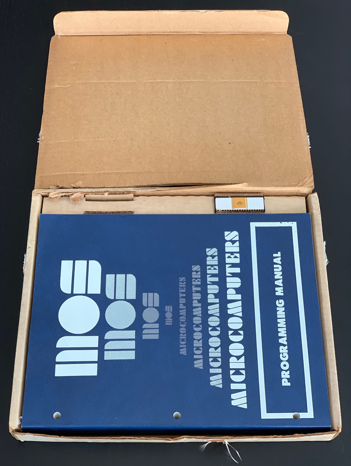
New In Box MOS MCS6502 CPU from 1975 (Michael Steil – pagetable.com)
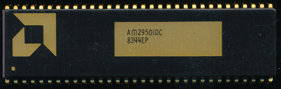
Today most all processors are permanently installed in their device (soldered in) or were taken from a bulk tray and installed by the OEM such as Dell or HP. AMD has, at least with their higher end CPU’s gotten quite creative with the marking on the chip itself, and both AMD and Intel still offer some pretty amazing retail packaging for their enthusiast processors (the i9 in a dodecahedron package is pretty cool). There was a time when almost all processors were available in retail packaging. This was the time of physical computer shops, largely bypassed now by the Internet, where the packaging of a processor helped sell it.
I collect such New In Box (NIB) processors as they are pretty need to see the branding/marketing that went with the CPU’s of years past, and was reminded of this when I saw perhaps one of the oldest NIB CPU’s I have ever seen on Michael Steil’s pagetable.com blog. An original MOS 6502 processor from 1975 in its original shipping box, as close to NIB as one can get. MOS’s packaging would make Apple proud with its simplicity and design keeping everything tidy and the MCS6502 visible as soon as the box is opened (I am happy they didn’t use miserable black foam either, so the CPU is pristine after 45 years). Even the original invoice is included. $25 for the CPU ($118 in 2019 dollars) and $10 (nearly half the cost of the CPU ($47 in 2019)) for documentation)
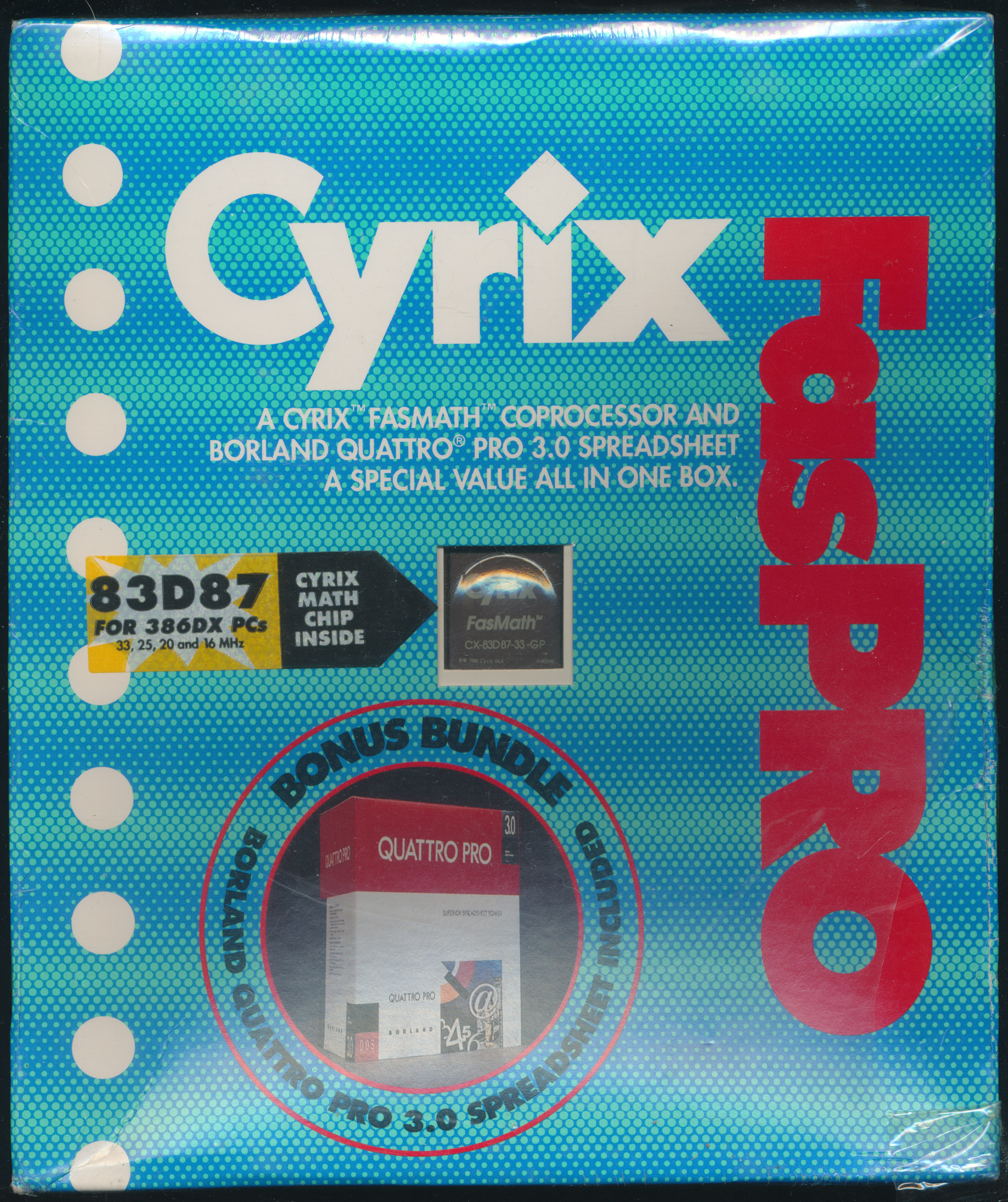
Cyrix 83D87 386 FPU Bundled with Borland Quattro PRO Spreadsheet software (a big thing back in 1992)
Intel started offering retail boxed CPUs with the 8087 coprocessor. This was really the first chip designed as a user upgrade to their PC (a new thing back then). Before this Intel’s closest thing to a NOB was University Kits or Dev Kits for various chips/processors. With the introduction of the PC, and the many thousands of beige box clones that followed, people themselves began buying processors and building computers for themselves at a much greater pace then before. There was many companies making compatible processors at the time so packaging helped set them apart. This began with upgrade products, math coprocessors for the 808x, 286 and 386 were the most common (by Intel, AMD, IIT, ULSI. Cyrix and more), but eventually processors themselves started getting the NIB treatment, Intel made OverDrive processors (still technically an upgrade product) for the 486. followed by actual Pentium CPUs in the retail box. By the late 1990’s everything from Celerons to Xeon server processors could be had in Retail box. Buying a retail boxed Xeon for your rackmount server seems like an odd thing to do, but apparently Intel figured it would need to be done.
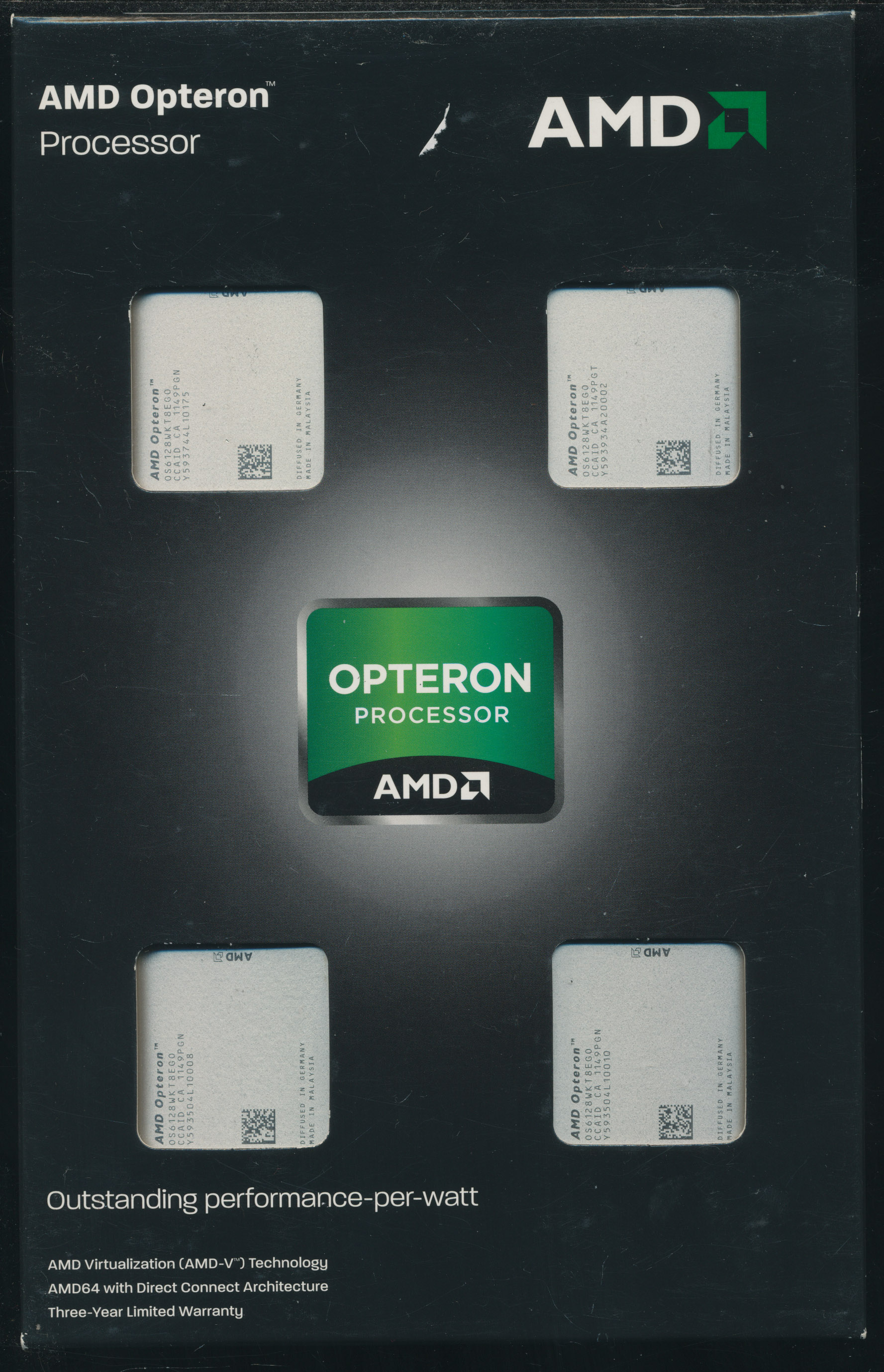
Quad AMD Opteron 6128s in Retail Box
Other companies such as AMD, Cyrix and VIA made NIB processors but they are much less common, and in a lot of ways more interesting. AMD made retail Durons, Athlons, and Opterons, and in one of the most unusual things I have seen for a NIB, an actual 4-pack of Opteron 6128s (pictured). The Opteron 6128 is a 8 core Magny-Cours server processor introduced in 2009 and cost $266 each at that time. This NIB set is dated late 2011, so would probably be a bit cheaper, but still $800 or so, and the large SWATX motherboards needed to run 4 socket G34 processors require somewhat special cases and PSU’s, but at least you can have a half terabyte of RAM. Inside the retail box is 4 smaller boxes, each containing an Opteron 6128 CPU, installation instructions, warranty info, and a case badge (you get 4 total case badges). It seems this packaging was designed to support different configurations (probable a single Opteron 6128, and duals).
Posted in:
CPU of the Day