January 24th, 2020 ~ by admin

ARMing the Modems of the 1990’s

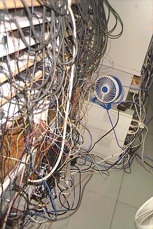
Racks of external modems at an ISP back in the day

Back in the 1990’s I worked at several ISP’s in my hometown.  These were the days of dial up, and by working at the ISP I got free dial up access which my family and I enjoyed.  We had several racks (white wire racks) of external modems for dial in.  This was the most common solution for smaller ISPs.  External modems were usually more reliable, cheap and easy to replace if/when they failed (and they did).  They got warm so it wasn’t uncommon to see a fan running to help move more air.  Surprisingly I could only find a few pictures of a such installations but you get that idea.

By the late 1990’s as dial in access and ISPs grew to be major concerns dial up solutions became much more sophisticated.  Gone were wire racks of modems and in were rackmount all in one dial in solutions.  These included boards that hosted dozens of modems on one PCB. with their own processing and management built in.  One of the largest companies for these solutions was Ascend Communications.  Their ‘MAX TNT’ modem solution once boasted over 2 million dial up ports during the 1990’s.  Such was Ascends popularity that they merged with Lucent in 1999, a deal that was the biggest ever at its time, valued at over $24 Billion ($37 Billion in 2020 USD). It wasn’t just traditional ISPs that needed dial up access, ATM’s and Credit Card processing became huge users as well.  It wasn’t uncommon to try to run a credit card at a store in the 1990’s and have to wait, because the machine got a busy signal.  The pictured Ascend board has 48 modems on a single PCB, and would be in a rack or case with several more boards, supporting 100s of simultaneous connections.

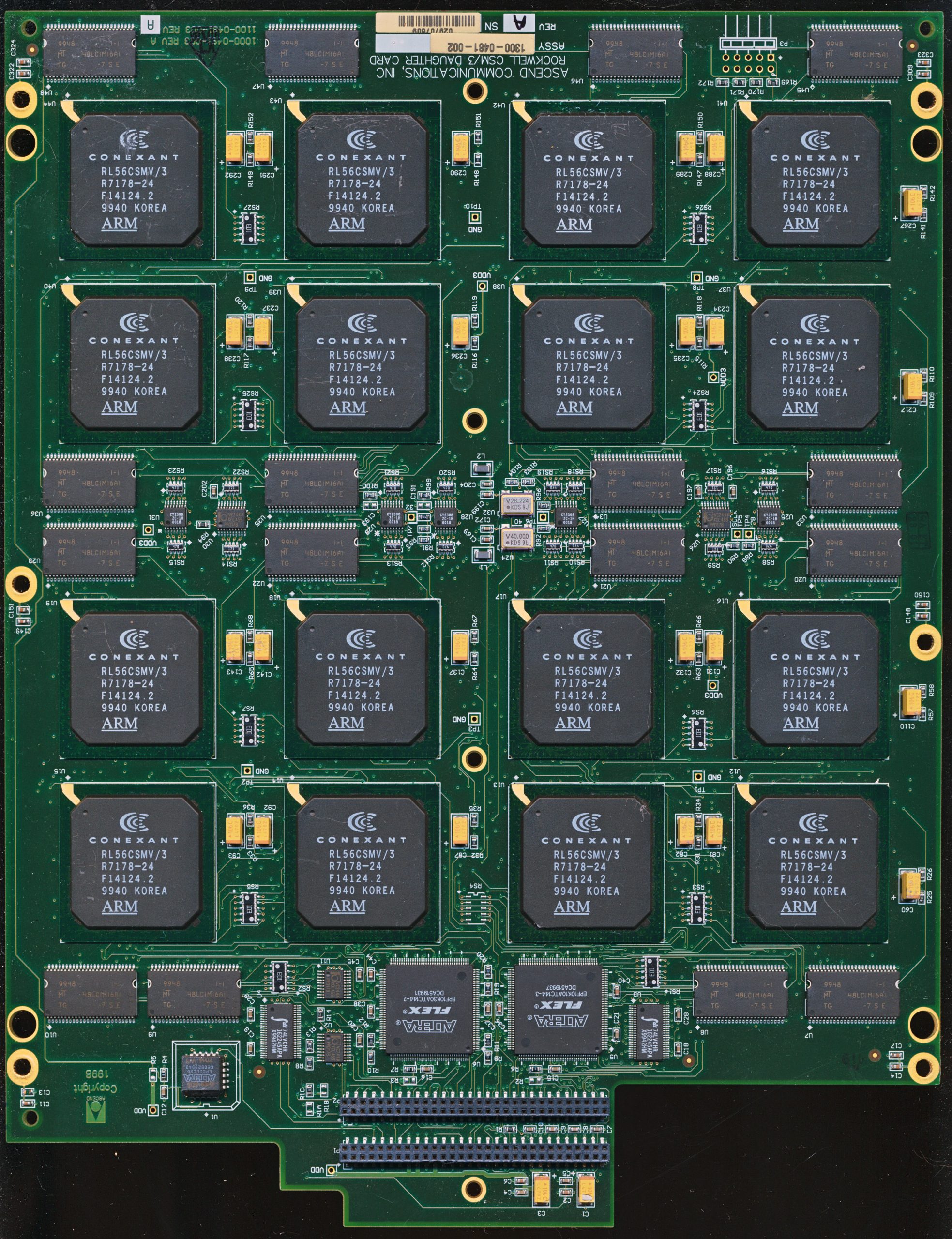
Ascen CSM/3 – 16x Conexant RL56CSMV/3 Chips provide 48 modems on one board.

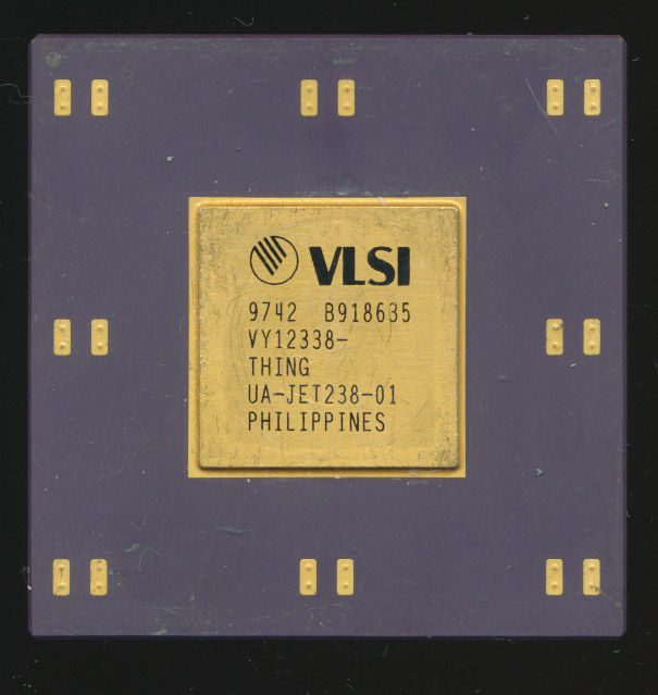
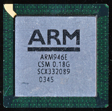
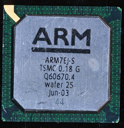
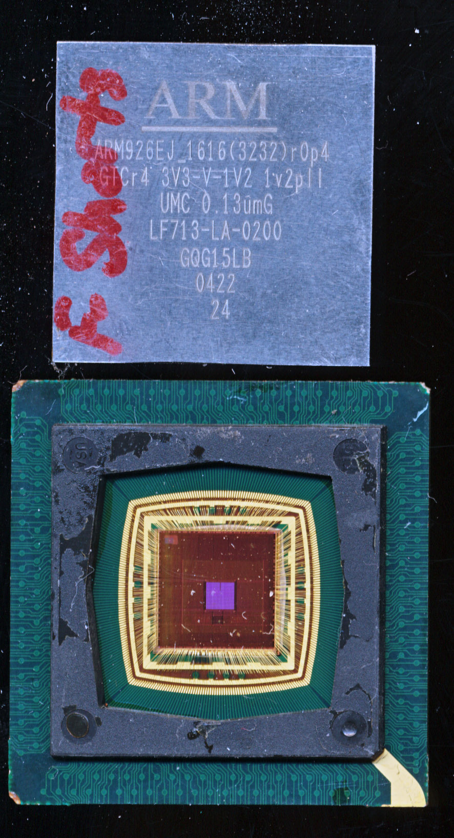
Ascend’s technology was based primarily on modem chips provided by Conexant (Rockwell Semiconductor before 1999).  Rockwell had a long history of making modem controllers, dating back to the 1970’s.  Most of their modem controllers up through the 80’s and early 90’s were based on a derivative of the 6502  processor.  This 8-bit CPU was more the adequate for personal use modems up to 33.6kbaud or so, but began to become inadequate for some of the higher end modems of the 1990’s.  These ran at 56k, supported various voice. fax, and data modes and handled a lot of their own DSP needs as well.  Rockwell’s solution was to move to an ARM based solution, and integrate everything on chip.

One of the results of this was the Anyport Multiservice Access Processor. It was called the Multiservice Access Process because it handled, voice, data, 33.6/56k, ISDN, cellular, FAX and several other types of data access, and it did so in triplicate.  The RL56CSMV/3 supported 3 different ports on one chip.  The CSM3 series was the very first ARM cored device Rockwell produced.  Rockwell had licensed the ARM810 (not very common), the ARM7TDMI and a ‘future ARM architecture’ (which was the ARM9) back in January of 1997.  In less then two

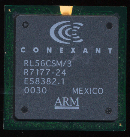
Conexant RL56CSM/3 R7177-24 ARM7 (non-V version has no voice support)

years Rockwell had designed and released the first AnyPort device, remarkable at the time.  The CSM/CSMV used the ARM7TDMI running at 40MHz and made on a 0.35u process.  The CSM/CSMV has another interesting feature, and thats the backside of the chip….

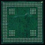
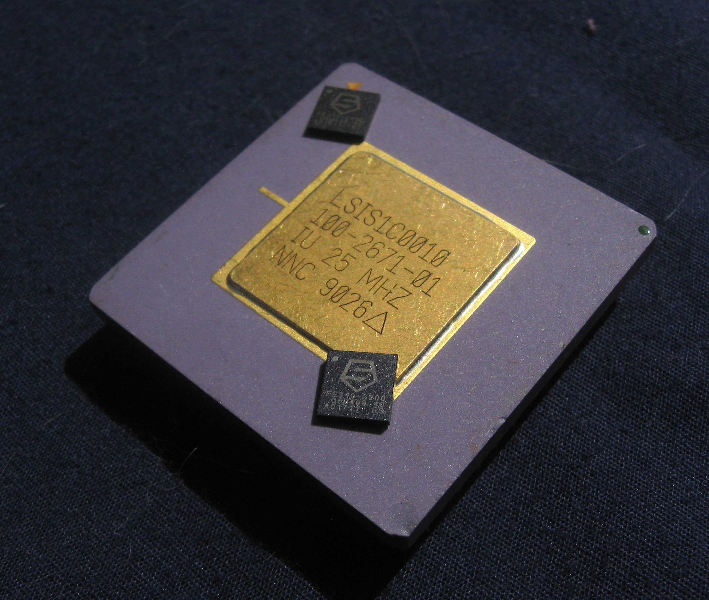
Take a look of the backside of the 35mm BGA chip, the ball arrangement is very unusual!  There is a ring of balls around the outer edge and 4 squares of 16 balls inside of that.  This is a multi-die BGA package.  There are 4 die inside one BGA package, three dies for the 3 Digital Data Pumps (DDPs) and a seperate die for the ARM7 MCU (which is made on a different process then the mixed signal DDPs).  Most of the balls in the 16×16 squares are to be connected to GND, and used for thermal dissipation (dissipating heat via the main PCBs ground plane).  Its not uncommon to see multidie packages today, but a multi die BGA package in 1999 was fairly innovative.

Surprisingly many of these chips are still in service, in today’s world of high speed broadband connections there are still many who are stuck on dial up.  As recently as 2015 AOL was still serving 2.1 million dial up customs in the US (out of around 10 million dial up customers total), which was still netting the company nearly half a billion dollars a year (by far their largest source of revenue at the time.  There is also still plenty of other infrastructure that still rely on dial up, ISDN, and even FAX services that require end point connections like the CSMV so its end is probably still a long ways off.

Tags:
, ,

Posted in:
CPU of the Day

October 12th, 2018 ~ by admin

Xilinx gets ARMed up for Free

Xilinx Virtex II Pro FPGAs from the 2000’s included embedded PowerPC processor cores.

Recently ARM announced they would be providing IP for the Cortex-M1 and M3 cores for free for users of Xilinx FPGA’s.  The Cortex-M1 and M3 are some of the most basic ARM cores, taking 12-25,000 gates for the Von Neumann architecture M1 and around 43,000 for the full up Harvard architecture M3 (with full ARM THUMB instruction set support).  Xilinx already offers FPGAs/SoCs with built in ARM cores, the SYNQ series is available with a variety of high end ARM cores such as the Cortex-A53 and the RF focused R5 core.  These obviously are fairly high gate county, and cost cores, where as the M1 and M3 cores are being provided without license, and without any royalties.  Drop in the IP into your FPGA design and go.

ARM and Xilinx say this is to meet the needs of their customers, who want to be able to use the same ARM architecture in their FPGA designs as in ASICs etc, and at the lowest investment in time and cost.  This certainly makes sense, having a free ARM core is better then a low cost ARM core, and removing the ‘paperwork’ hassle helps, but that’s probably not the only reason ARM is doing this, and doing it specifically for Xilinx.

There are a couple other things at play here, ARM Mx cores are basic RISC processors, used for when you just need to get some basic processing done, no frills, low power, and easy to use.  It turns out that’s a market that is now seeing some competition from the SiFive RISC-V core.  This is a basic, easy to use RISC core, that is synthesizable into ASICS, and FPGAs, and comes with a one time low cost license fee and no royalties.  Its being used by such heavyweights as Nvidia, and could threaten the Cortex-Mx domain, so it makes sense for ARM to offer, essentially their introductory processor core, for free, as a way to sway people to the ARM ecosystem.  But why Xilinx?

Perhaps Xilinx is just the start of ARM’s plans, Xilinx is one of the biggest providers of FPGAs in the world so certainly that will help keep people in the ARM. Xilinx infact, already has a drop-in 32-bit RISC processor core available to all their customers, the MicroBlaze and PicoBlaze, of their own design.  There are also drop in 80C186 cores, MCS-51 cores, the LEON SPARC core and many others. The other big name in FPGAs is Altera, a company that has competed with Xilinx for the better part of 30-years and was, in June of 2015 bought by none other then Intel.

Altera has had a close relationship with Intel since the 1980’s when Intel first started assisting Altera with fab’ing their PLDs.

This gave Altera greater access to Intel’s fab/engineering prowess, but also to all of Intel’s IP.  Is Intel going to offer free ARM cores on Altera FPGAs (the Stratix/Arria series does include hard Cortex-A9/A53 cores already)?  It seems unlikely that they would work to support their architectural competitor any more then they have to.  It is more likely that Intel would offer some form of 32-bit x86 processor core for their FPGAs.  Now x86 isn’t exactly known for low gate counts, but it is possible.  Currently softcore 8086 and 80186 processor (the Turbo86 and Turbo186) are 22,000 and 30,000 gates respectively, really a rounding error in FPGAs that now have millions of gates. More and more, FPGAs are becoming less FPGA like, and more ‘configurable processor’ like.

October 14th, 2017 ~ by admin

VLSI: What is this THING?

VLSI VY12338 THING UA-JET238-01 – Made in 1997

VLSI was started back in 1979 by several former Fairchild employees, 2 of which had previously founded Synertek, a connection that becomes important later on.  VLSI is best known for being a contract deign/fab services company.  They excelled at custom, and semi-custom designs for a wide range of customers, as well as acting as a foundry for customers own designs.  They became best known for their part in the development and success of the ARM processor back in the late 1980’s with ACORN.  They manufactured, as well as marketed and sold, several versions of the ARM processor, one of the few processors they actually sold themselves.  They also made a 6502 used by Apple and 65C816 (CMOS 16-bit 6502).  The 6502 was also a processor that Synertek had made back before Dan Floyd, and Gunnar Wetlesen left Synertek to start VLSI.

VLSI went on to fab processors for some of the biggest companies of the 1980’s.  The made the processor for several Honeywell BULL mainframes, built the processor for the HP A990 computer, and made dozens of chips for SGI and WANG.  VLSI also enjoyed wide success in the early 1990’s making chipsets for 486 processors, before Intel began to offer chipsets on their own in the Pentium era.

Unfortunately like LSI, most of VLSI’s designs are relatively unknown to all but them and their customer.  Marking on the chips rarely provide information on who it was made for, and even less on what exactly it does.  The above chip, marked “VY12338 THING UA-JET238-01” seems to be names as an answer to the question “What do we call this thing?”  Certainly seems to be a bit of humor on the part of some engineer.

VLSI was bought by Philips (now NXP) in 1999 so the THING may forever remain an unknown thing.

Tags:
, ,

Posted in:
Just For Fun

June 5th, 2017 ~ by admin

SiFive FE310: Setting The RISC Free

SiFive FE310 RISC-V Processor. Early LSI SPARC Processor for size comparison. Both are based on U.C. Berkeley RISC designs.

The idea of RISC (Reduced Instruction Set Computer) processors began in education, specifically University of California, Berkeley in the early 1980’s, and it was out universities that some of the most famous RISC designs came.  MIPS, still in use today, started life as a project at Stanford University, and SPARC, made famous by Sun, and now made by Oracle and Fujitsu, started life as a Berkeley University project.  Universities have continued to work with RISC architectures, for research and teaching.  The simplicity of RISC makes them an ideal educational tool for learning how computers/processors function at their basic levels.

By the late 1980’s RISC had begun to become a commercial revolution, with nearly every player having their own RISC design.  AMD (29k), Intel (i960), HP (PA-RISC), Weitek (XL8000), MIPS, SPARC, ARM, Hitachi (SH-RISC), IBM (POWER), and others offered their take on the RISC design.  Most were proprietary, while a few were licenseable, none were open architectures for anyone to use.

Unfortunately, outside of the university, RISC processors are not as simple.  The architectures, and their use may be, but licensing them for the design is not.  It can often take more time and effort to license a modern RISC processor then it does to actually implement it.  The costs to use these architectures,both in time and money often prohibit their very use.

SiFive FE310 – Sample Donated by SiFive. Full 32-bit RISC on a 7.2mm2 die in a ~36mm2 package

It is out of this that SiFive began.  SiFive was founded by the creators of the first commercially successful open RISC architecture, known as RISC-V.  RISC-V was developed at Berkeley, fittingly, in 2010 and was designed to be a truly useful, general purpose RISC processor, easy to design with, easy to code for, and with enough features to be commercially useful, not limited to the classroom.  It is called the RISC-V because it is the fifth RISC design developed at Berkeley, RISC I and RISC II being designed in 1981, followed by SOAR (Smalltalk On A RISC) in 1984 and SPUR (Symbolic Processing Using RISC) in 1988.  RISC-V has already proved to be a success, it is licensed freely, and in a way (BSD license) that allows products that use it to be either open, or proprietary.  One of the more well known users is Nvidia, which announced they are replacing their own proprietary FALCON processors (used in their GPUs and Tegra processors) with RISC-V.  Samsung, Qualcomm, and others are already using RISC-V.  These cores are often so deeply embedded that their existence goes without mention, but they are there, working in the background to make whatever tech needs to work, work.

The RISC-V architecture supports 122 instructions, 98 of which are common to almost all prior RISC designs and 18 common to a few.  Six completely new instructions were added to handle unique attributes of the architecture (using a 64-bit Performance Register in a 32-bit arch.) and to support a more powerful sign-injection instruction (which can be used for absolute value, among other things). It uses 31 32-bit registers (Register 0 is reserved for holding the constant ‘0’) with optional support for 32 floating point registers.  True to the RISC design, it is a pure Load/Store processor, the only accesses to memory are via the Load/Store instructions.

Intel 4004 with 5 SiFive RISC Processors. The 4004 was meant for a calculator. The FE310 is meant for whatever your mind may dream up.

SiFive is unique among RISC IP companies.  They not only license IP but also sell processors and dev boards.  The FE310 (Freedom Everywhere 310) is a 320MHz RISC-V architecture with 16K of I-cache and 16K of scratchpad RAM fabbed by TSMC on a 180nm process. Even on this process, which is now a commodity process, the FE310’s efficient design results in a die size of only 2.65mm x 2.72mm.  On a standard 200mm wafer , this results in 3500 die per wafer, greatly helping lower the cost.  Its an impressive chip, and one that is completely open source.  What is more impressive is licensing SiFive cores, it is a simple and straightforward process.  The core (32 bit E31 or 64-bit E51) can be configured on SiFive’s site, with pricing shown as you go.  The license is a simple 7 page document that can be signed and submitted online.  Pricing starts at $275,000 and is a one time fee, there are no continuing royalty payments.  The entire process can be completed in a week or less.

In comparison, ARM, the biggest licensor of RISC processors, does not publish pricing, charges 1-2% royalties on every chip made, and has a license process that can take over a year.  The base fees start at around $1 million and go into the 10’s of millions, depending on how you want to use the IP, where it will be, and for how long.  For many small companies and users this is simply not feasible, and it is these smaller users that SiFive wishes to work with.  Licensing a processor for the next great tech, should not be the hurdle that it has become.  Many great ideas never make it to fruition due to these roadblocks.  We look forward to finding SiFive processors and cores in all sorts of products in the future.

Thanks to SiFive for their generous donation of several FE310 processors to the CPU Shack Museum.

Tags:
, , , ,

Posted in:
CPU of the Day

February 19th, 2017 ~ by admin

Milandr K1986VE91T – The ARM of Russia

Milandr K1986VE91T – 80MHz ARM Cortex-M3

In the early 1990’s a Milandr was formed in Zelenograd, Russia (just a short distance to the NW of Moscow), the silicon valley of Russia, home to the Angstrem, and Micron IC design houses. They are a fabless company, though with their own packaging/test facilities, specializing in high reliability metal/ceramic packages. Most of their products are fab’d in Germany, by X-Fab.  X-Fab was formed in part, from the remains of the Soviet/E. German era VEB Mikroelektronik Karl Marx, in Erfurt Germany, also known as FWE/MME and later Thesys.  In Soviet times it wasn’t uncommon for Soviet companies to use dies produced by FWE in their own packages, so this bit of legacy continues today.

The K1986VE91T is one of Milandr’s top end products, it is an 80MHz ARM Cortex-M3 based processor, and likely one of the largest, if not the largest, Cortex-M3 made.  It is made on a 180nm process and includes 32K RAM, 128K FlashROM, 96 USER I/O, USB, 2 UART and 12-bit DAC/ADC.  Judging by the die, the processor was built with standard licensed blocks, very common for such designs.  Milandr licensed the ARM Cortex-M3 itself in December of 2008, for use mainly in automotive and industrial applications. Milandr is also the very first Russian company to license and use an ARM core.

Analog Devices ADUCM322BBCZ ARM Cortex-M3 80MHz – Same basic core, but in a very much less appealing package

The package, however, is completely unique.  It is a 132 pin CQFP package. There are 33 gold leads on each side of the white ceramic package.  Each row is actually 2 staggered rows, the offset allows the finer lead pitch, and still room to bond the leads to the top of the package.  Soviet processors were often delivered in the most stunning of packages and 25 years later, Milandr keeps that tradition alive.

Each of these processors came with a brief datasheet, complete with inspection stamps for the processor. It is all in Russian, but check it out here.

Milandr made several variations of the Cortex-M3, including the VE92 and VE93 which are internally identical, but with much less I/O available owing to there smaller 64 pin and 48 pin packages respectively. Milandr also made a copy of the PIC17 processor that we covered last year.

A version of the K1986VExx continues to be made by Milandr, but renamed to the MDR32F9Qx.  It continues to have the same basic core, but in a 144 pin package, allowing even greater I/O support.


Tags:
, ,

Posted in:
CPU of the Day

October 4th, 2016 ~ by admin

Testing all the ARMs

ARM946E on a Chartered Semiconductor 0.18u Process

ARM946E on a Chartered Semiconductor 0.18u Process

ARM is one of the most popular RISC cores used today, and has been for over a decade now.  ARM is an IP company. They license processor designs/architectures for others to use, but do not actually manufacturer the processors themselves….or do they?

ARM offers a variety of cores, and licenses them in a variety of different ways.  There are, in general, three main ways to get an ARM design.  Larger companies with may resources (such as Apple, Broadcom, or Qualcomm) will purchase an ARM architecture license.  This isn’t specific to any ARM core in particular (such as say a ARM946) but the entire ARM architecture, allowing these companies to design their own ARM processors from the ground up.  This takes a lot of resources and talent that many companies lack.

Second, ARM offers RTL (Register Transfer Level) processor models, these are provided in a hardware programming language such as VHDL or Verilog.  They can be dropped into a design along with other IP blocks (memory, graphics, etc) and wrapped with whatever a company needs.  This is a fairly common method, and typically the lest expensive.  It does require more work and testing though.  Designing a chip is only part of the process. Once it’s designed it still must be fab’d.

ARM7EJ-S on a TSMC 0.18u Process. Wafer #25 from June 2003

ARM7EJ-S on a TSMC 0.18u Process. Wafer #25 from June 2003

ARM also offers ARM models that are transistor level designs, pre-tested on various fab processes.  Pre-tested means exactly what it sounds like. ARM designed, built and had them manufactured, fixing any problems, and thus giving the ability to say this core will run at this speed on this fab’s process.  Testing and validation may often go as far as testing a particular fab’s particular process, in a particular package.  Its more work, and thus cost more, but these make for drop in ARM cores. Want to use a ARM946 core, on a TSMC 0.18u process in a lead free Amkor BGA package? Yah ARM’s tested that and can provide you with a design they know is compatible.  This allows extremely fast turn around from concept, to design to silicon.

In the below picture (click to enlarge) you can see a large variety of ARM cores from the early 2000’s. They span ARM7, ARM9, ARM10 and ARM11 designs.  Each is marked with info as to what exactly it is.  The core name, the revision (such as r2p0, meaning major revision 2, pass/subversion 0) as well as the Fab (TSMC, UMC, SMIC, Chartered) and the design node (all of these are either 0.18 or 0.13u processors).

21 Various ARM design tet chips from TSMC, UMC, Charted, covering many ARM cores.

21 Various ARM design tet chips from TSMC, UMC, Charted, covering many ARM cores.

Also noted on some is the exact wafer the die was cut from, this is typical on VERY early production tests, usually first run silicon, so they can identify any physical/manufacturing defects easier.  Some design modifications have little to do with the processor itself, but are done to increase yields on a given process/node.

ARM926EJ on a UMC 0.13u Process. THe package has a removable die cover.  Note the large die, thought he processor core itself is very small (its in the upper left)

ARM926EJ on a UMC 0.13u Process. 

Package type (in this case most are Amkor BGA) and other features are noted.  Many say ‘ETM’ which is ARM’s Embedded Trace Macrocell, a debugging tool that allows instruction and date traces of an in operation core, very useful for debugging. ARM offers ETM for each of their processor types (ETM9 for example covers all ARM9 type cores) and itself has a revision number as well.

Some of these chips come in an interesting BGA package. The package has a removable die cover for inspection/testing (and possibly modification). Note the large die in the ARM926EJ on the left, though the processor core itself is very small (its in the upper left only a few square mm).  This is done to facilitate bonding into the package, In this type of package there wouldn’t be any way to connect all the bonding wires to the very tiny ARM core, so the die has a lot of ‘wasted’ space on it.

So does ARM make processors? Yup! but only for internal use, to help develop the best possible IP for their clients.


Tags:

Posted in:
CPU of the Day

February 8th, 2016 ~ by admin

Reverse Engineering the ARM1 Processor

VLSI VL2333-QC ARM ACORN - ARM2 (Adds MULT instruction in hardware) 1987

VLSI VL2333-QC ARM ACORN – ARM2 (Adds MULT instruction in hardware) 1987

Ken Shirriff has an interesting article on reverse engineering the original ARM1 processor (as designed by ARM, and implemented by VLSI).  He goes right to the silicon to form a transistor level model/emulator of the chip.  Back in 1986 when the ARM was designed and released, it wasn’t very well known, being used in very few devices.  This continued for over a decade surprisingly. being used in niche markets (the Apple Newton, the DEC StrongARM on RAID cards, etc).  It wasn’t until the 2000’s that this processor startup from England became the powerhouse it is today.  Two major developments drove this, mobile, and multimedia.  The ARM architecture was powerful, small, and easy on the power budget, this obviously was a benefit for mobile, but also proved very useful in dealing with multimedia processing, such as controllers on DVD players, digital picture frames, MP3 players and the like.  Today, hundreds of companies license and use the architecture and it is found in devices now numbering in the billions.

Tags:

Posted in:
Research

May 28th, 2014 ~ by admin

Intel Joins Forces with Rockchip – ARM Meets x86

rockchip logoIt’s well known that Intel missed the jump on tablet and phone processors.  Intel sold off their PXA line of ARM processors to Marvell in 2006, in an attempt to ‘get back to the basics.’  It turned out that this sale perhaps was a bit premature, as the basics ended up being mobile, and mobile is where Intel struggled (by mobile we mean phones/tablets, not laptops, which Intel has no problems with).

In January of 2011 Intel purchased the communications division of Infineon, gaining a line of application and baseband processors, based on ARM architecture of course.  Intel developed this into the SoFIA applications processor, which was ironically fab’d by TSMC.   Eventually the designs would be ported to Intel 14nm process, or that was the plan.

Intel Atom - Now by Rockchip?

Intel Atom – Now by Rockchip?

So this weeks announcement that Intel has signed an agreement with the Chinese company Rockchip, to cooperate on mobile applications processors is a bit of a surprise, but the details show that it makes sense.  Rockchips current offerings are ARM based, much as Intel’s current SoFIA processor, as well as Apple Ax series, Qualcomm’s SnapDragon, TI’s OMAP, etc. However, the agreement with Rockchip is not about ARM, its about x86.  For the first time in many years Intel has granted another company an x86 license, specifically, Intel will help ROckchip build a quad-core Atom based x86 processor with integrated 3G modem.  Rockchip currently uses TSMC as their fab, however also with this agreement Rockchip gets access to Intel 22nm and 14nm fab capacity.

Who wins?

Read More »

March 6th, 2014 ~ by admin

The Agilent ARM701 Processor

ARM 701 mis-print on the left

ARM 701 mis-print on the left

We recently received several Remote Server management cards, powered by the Agilent (spun off of HP in 1999) N2530 SoC.  This SoC provides the processing for remotely administering, and managing servers.  At its hearts is an ARM processor running at 33MHz.  Proudly marked on the chip, is ‘ARM 701 POWERED.’  There is one problem, there never was an ARM701 processor core.  The N2530 is in fact powered by an ARM710.  A typo was made when marked the Rev D chips, and later fixed on the Revision E.  I have not yet received an example of a Rev C (or earlier) to see if they too have this error, but E and later certainly did not.  The Agilent N2530 was used for many years in the early 2000’s on cards by Dell, Fujitsu, and IBM (and likely others).  Essentially forming a computer within a computer, these cards often had their own graphics support (ATI Mobility Radeon, among others) as well as support for CD-ROMs, hard drives, LAN (for access) and everything else you would find in a stand alone computer.  Typically they could remote start, reboot, and power down servers, all over a network connection.

Tags:
,

Posted in:
CPU of the Day

February 27th, 2014 ~ by admin

The Unlikely Tale of How ARM Came to Rule the World

Bloomberg Business Week recently published an interesting article on ARM’s rise to power in the processing world.  There first major design ‘win’ was a failed product known as the Apple Newton, yet they would go on to become a powerhouse that is no challenging Intel.

In ARM’s formative years, the 1990’s, the most popular RISC processor was the MIPS architecture, which powered high end computers by SGI, while Intel made super computers (the Paragon) based on another RISC design, the i860.  Now, nearly 2 decades later, after Intel abandoned their foray into the ARM architecture (StrongARM and X-Scale) RISC is again challenging Intel in the server market, this time, led by ARM.

MIPS, now owned by Imagination, is again turning out new IP cores to compete with ARM, and other embedded cores.  Their Warrior class processors are already providing 64-bit embedded processing power, though with a lot less press that the likes of Apple’s A7.

Tags:
,

Posted in:
Processor News