
The History of Angstrem Memory IC’s in the USSR
This article is about memory chips manufactured by one of the entities – the leader of the electronic industry of the USSR – Angstrem. As you know, the Soviet Union ceased to exist in December 1991. We restrict ourselves to the development period of the considered memory chips produced at Angstrem, the end of 1991. Let’s make an attempt to track how the capacity of memory chips grew, how technologies were improved that allowed the Soviet Union not to let the world leaders in electronics go far from itself at that time. A small example: Angstrem’s Dynamic RAM 4K went into mass production in mid-1975, Intel introduced its own in 1974. Intel launched a 16K DRAM in 1977, and Angstrem released its counterpart in 1978.
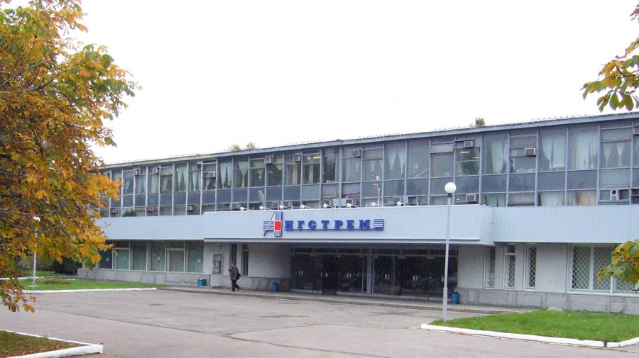
Angstrem Headquarters
Angstrem was established in June 1963 in Zelenograd (outside of Moscow) as a pilot plant in conjunction with the Scientific Research Institute of Precision Technology. At Angstrem, new technologies for the production of microelectronics were developed, and pilot batches of new microcircuits were also produced. The debugged production technology was then transferred to other enterprises of the USSR and countries of Eastern Europe.
The development and manufacture of memory chips was one of the main activities of Angstrem. It was on them that new semiconductor structures and production technologies were more effectively worked out, and the stability of obtaining finished products is considered in world electronics as a sign of technology ownership. It’s relatively easy to make a small batch of good chips, it’s hard to make a process whereby a large amount of chips can be made and be reliable. It was the very low chip yield percentage that played a cruel joke on Angstrem when mastering the production process of the DRAM 565RU7 chip.
SRAM
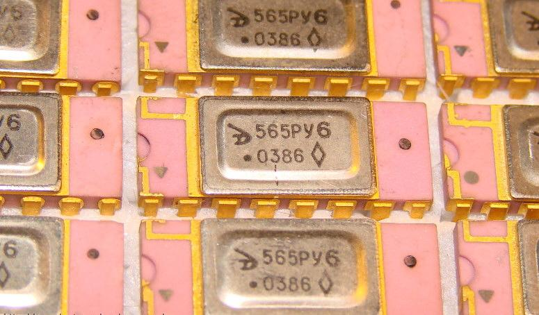
In 1966, Angstrem created the first MOSFET in the USSR, which was the first step towards the strict goal of creating CMOS integrated circuits. The first CMOS microcircuit, created in the Soviet Union in 1971, was the 16-bit Angstrom matrix of memory cells 1YaM881.The supply voltage is 6 volts instead of 5 volts, like the rest of the chips in this series.
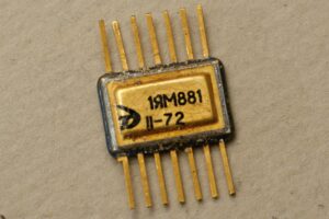
1YaM881 – 1972
The next in a series of static RAM chips was the CMOS K561RU2 (K564RU2), released in 1976. 564 series of chips is a “military” analogue of the 561 series. In these series, there are several dozen microcircuits. The chip has an organization of 256 words by 1 bit.
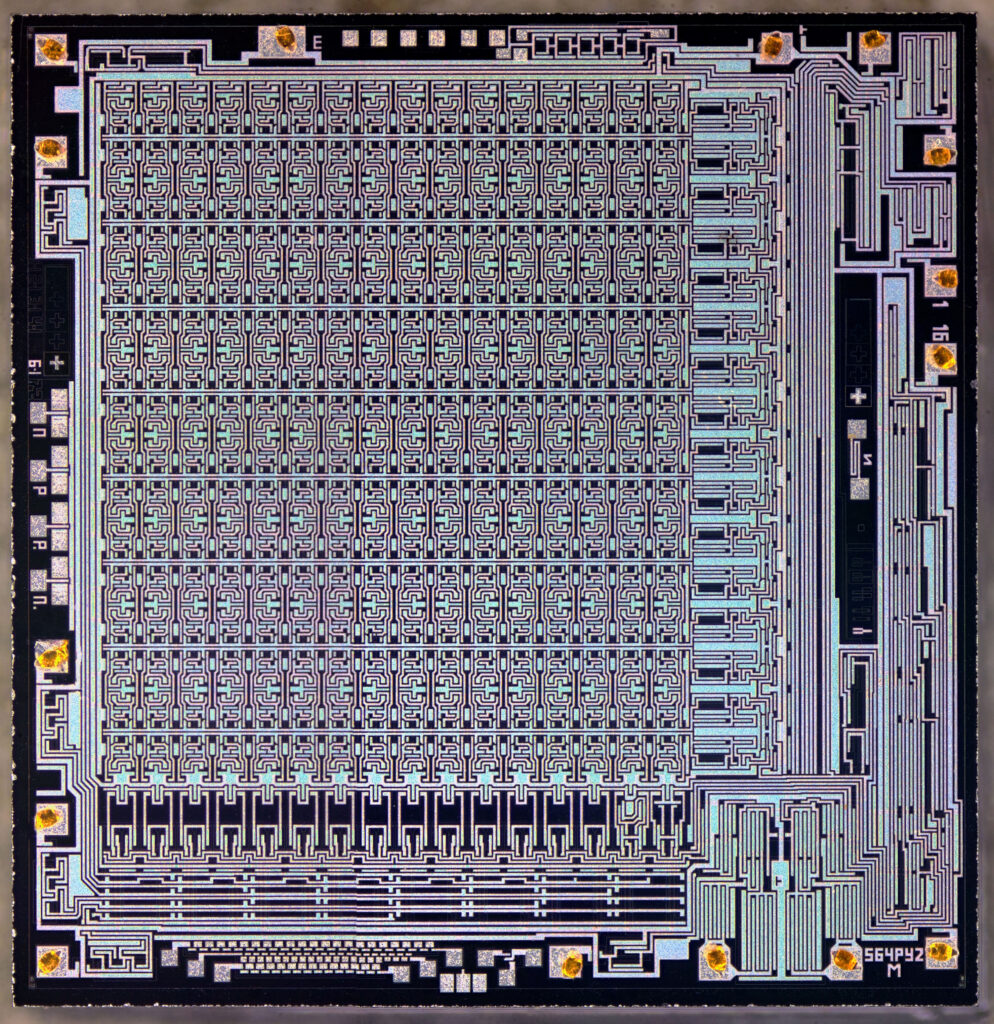
561RU2 die – 16×16 256bit matrix clearly visible – The image is taken from the site https://radiopicture.listbb.
It contains 2067 integral elements. Supply voltage is 3-15 volts. It’s an analogue of CD4061A. It should be noted that in most cases ‘analogue’ means similar to, not an exact copy or exactly compatible. The USSR did make some compatible IC’s, but they mostly made stuff that was similar, but built to their own specifications/needs.
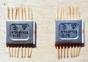 K564RU2A -1978 |
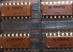 K561RU2 -1979 |
The package of the K561RU2 chip is wider than the standard packages of this series.
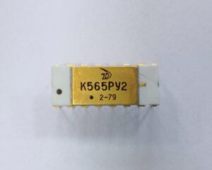
K565RU2 -1979
The K565RU2 static RAM chip was manufactured using NMOS technology. Chip capacity was 1024 bits (1024×1). Contains 7142 integral elements. An analogue of Intel 2102A, developed in 1974. K565RU2 appeared in 1977. It was originally designed to be placed in a ceramic package, but later, in order to reduce the cost of production, the dies began to be packed in plastic packages.
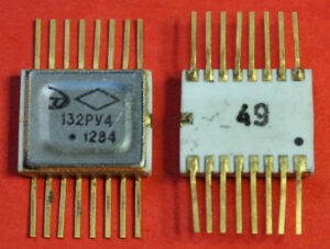 132RU4 |
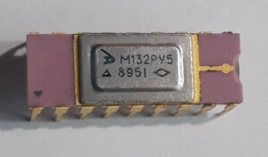 M132RU3 |
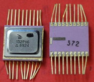 132RU6 |
Series 132 chips are static RAM, made by NMOS technology.
132RU4 – The organization of the chip is 1Kx1, analogue of Intel 2125AL, contains 7848 integrated elements.
132RU5 – The organization of the chip is 4Kx1, analogue of Intel 2147, contains 26584 integrated elements.
132RU6 – The organization of the chip is 16Kx1, analogue of Inmos IMS1400 , contains 122802 integrated elements.
These microcircuits were also produced in plastic packages.
A common disadvantage of memory on made on a NMOS process is a significant power consumption in the information storage mode. But for 132RU6, a multiple reduction in power consumption is possible by turning off the supply voltage, but keeping it at the level of 5V at the CS pin.
EEPROM
KM558RR3 is Electrically Erasable Programmable Read-only Memory chip. The peculiarity of this microcircuit is the erase voltage (18 volts) and the programming voltage (24 volts).There are no foreign analogues. The chip has a capacity of 8K x 8 bits, is made using NMOS technology, the supply (operating) voltage is 5V.
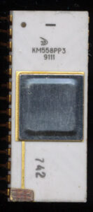
KM558RR3 1991
The minimum number of rewrite cycles is 100 which holds for the entire 558 series. A modern Atmel EEPROM cell is typically rated for 100,000 write cycles, a number that has held true since the early 1980’s.
UV-EPROM
The 573 chip series is the most common in the Ultra-Violet Erasable Programmable Read Only Memory chip series. The only microcircuit from the 573 series that Angstrem produced, the K573RF3, stands out for its more complex structure and advanced functionality compared to other microcircuits in this series. Its distinguishing feature is that it is adapted for direct operation with the Q-BUS, having the necessary built-in interface tools to ensure I/O compatibility with it. In addition, the chip has a built-in programmable address device, which allows you to combine up to eight chips into a ROM unit without additional equipment by connecting them to Q-BUS. Q-BUS was the standard DEC bus for the LSI-11 series of computers. Angstrem also was famous for its line of LSI-11 processors, thus their EPROMs being designed specifically tow work with them. We wrote about these Angstrem LSI-11 CPUs a while back.
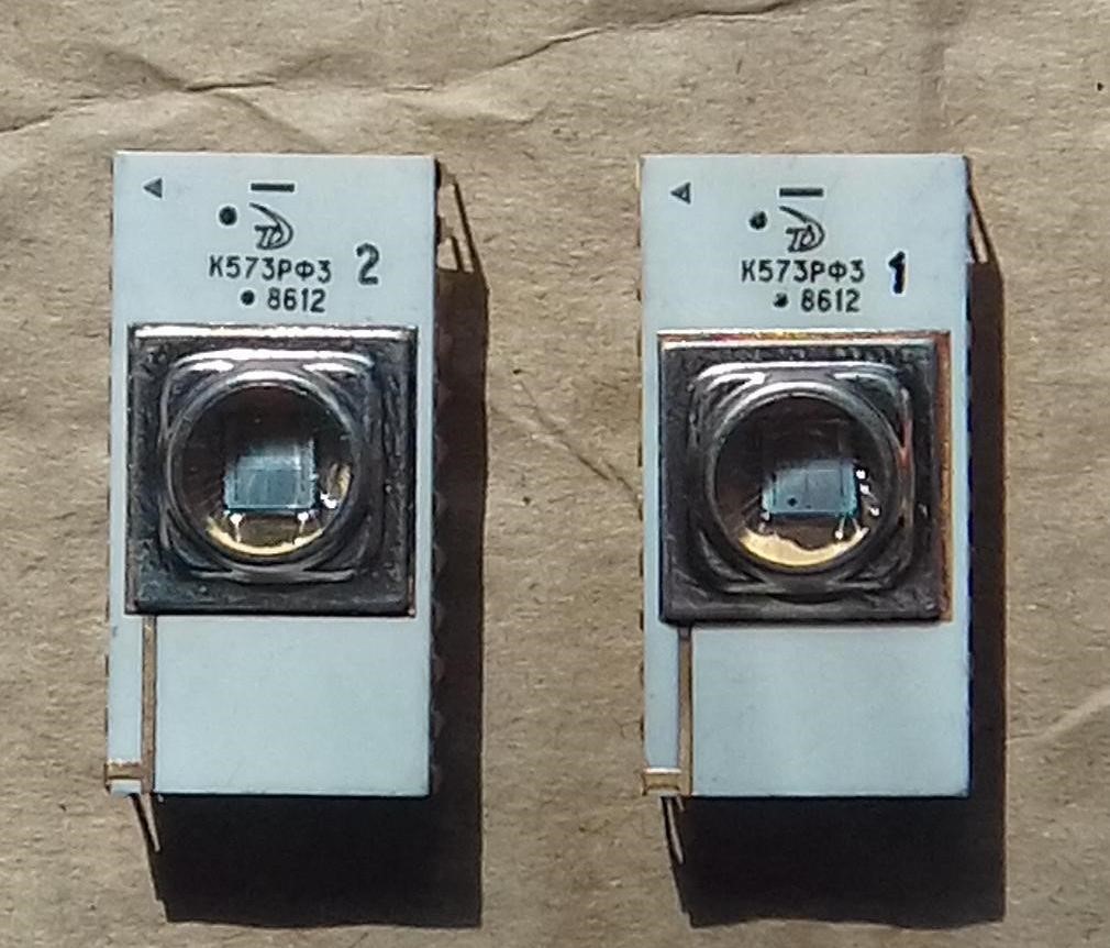
K573RF32 and K573RF31 – Both from 1986
Microcircuits are made according to NMOS technology, supply voltage 5V, programming voltage 18V, contains 140,000 integrated elements (K573RF3). The technological process of production was imperfect which often resulted in several cells on the die being defective. In this case, the manufacturer blocks access to the damaged part of the die by connecting one or two address inputs to ground or to the power supply output inside the microcircuit. Chips are obtained, the capacity of which is half or a quarter of the original. Angstrem marked microcircuits as follows:
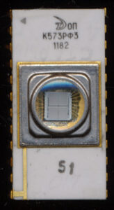
K573RF3 – 1982 – Sample
64 Kbit capacity (4096×16) K573RF3;
32 Kbit capacity (2048×16) for K573RF31, K573RF32;
16 Kbit capacity (1024×16) for K573RF33, K573RF34.
The number of rewrite cycles is minimal in the entire 573 series: only 10. Early Intel EPROM’s could manage 1000 cycles and more modern ones typically do 10,000 cycles.
It should be noted that Angstrem certainly wasn’t the only manufacturer to use defective dies. The same practice (and marking pattern) was used by Vostok. Nor was it limited to the USSR, Intel used bad 2708 dies to make the 2704.
DRAM
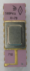
565RU1A Military grade
565RU1 is a 4096 bit DRAM chip with 4096 x 1 organization. Designed in 1975. It is a complete analogue of TMS4060 Texas Instruments, MM5280 National Semiconductor and Intel 2107A. Supply voltage – + 5V, + 12V, -5V. Package type – CDIP22. The first releases used a ceramic package with a width of 10mm, then, to reduce the cost, an epoxy-based package was developed with the same dimensions and pinout. It was the first DRAM microchip in the USSR manufactured using NMOS technology, as well as the first microchip comparable in parameters to foreign analogues.
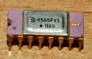
K565RU3 DRAM chip with a capacity of 16384 bits and an organization of 16384 x 1 bits. The prototype was the MK4116-4 chip from Mostek. Contains 68955 integral elements. Supply voltage +5V, +12V, -5V. The microcircuit was manufactured using NMOS technology.
The first releases used a 10 mm wide ceramic package, then, to better match the prototype, the width of the package was reduced to 7.5 mm (for MK4116, the width of the package is 7.62 mm). Unlike the prototype, the K565RU3 in a plastic package was not mass-produced.
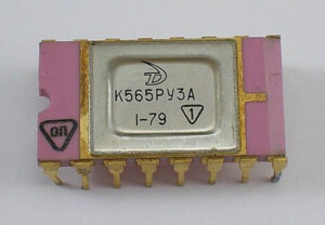 K565RU3А narrow package |
 K565RU3А standard package |
K565RU3 microcircuits are divided into groups (type ratings) that differ in access time characteristics. The fastest are in Group A, followed by Group B, and so on. One dot – group A, two dots – group B, three dots – group V. Microcircuits of group G were marked without a dot. The groups were named according to the letters of the Russian alphabet ( А(A), Б(B), В (V), Г(G), Д(D)).
| Group | Speed (ns) | Dots |
| A | 510 | 1 |
| B | 510 | 2 |
| V | 410 | 3 |
| G | 370 | None |
565RU6V Military grade -1988
The 565RU6 is a dynamic RAM with a capacity of 16384 bits (16K x 1), made on NMOS technology. It contains 74210 integral elements. Analog to the Intel 2118 with a supply voltage of +5V. The microcircuit was also produced in a plastic case. One dot – group V, two dots – group G. Microcircuits of group B were marked without a dot.
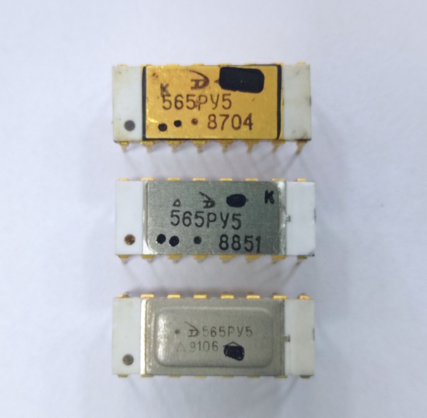
565RU5 Group G (3 dots) and Group B (no dot)
Chip 565RU5 is a dynamic RAM with a capacity of 64 Kb (64K x 1), NMOS technology. Contains 279618 integral elements. Analog 4164.
Chips 565RU5 and 565RU6 have the same electrical parameters, but different information capacity.
565RU5 has the following encoding:
| Group | Speed (ns) | Dots |
| B | 230 | None |
| V | 280 | 2 |
| G | 360 | 3 |
| D | 460 | 4 |
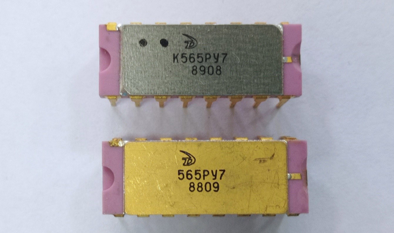
K565RU7 Group V (2 dots) and 565RU7 Group G (no dots)
The K565RU7 microcircuit is a DRAM with a capacity of 262144 bits and an organization of 262144 x 1 bit, made using NMOS technology. The number of integrated elements on a chip is 831550. 565RU7 is not an analogue of 41256 due to a different refresh scheme. 565RU7 has the following encoding:
| Group | Speed (ns) | Dots |
| V | 340 | 2 |
| G | 410 | 3 |
| D | 500 | None |
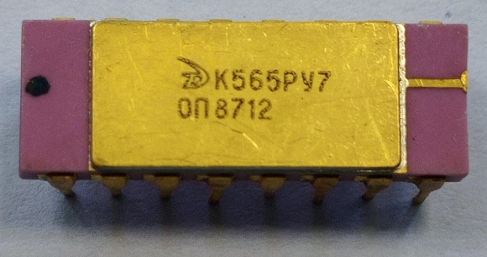
K565RU7 – 1987 -Sample
Work on the creation of 565RU7 in Zelenograd began in 1985. From 1986 to 1988, a very limited number of chips were produced. The chip yield rate was depressingly low. All 565RU7 microcircuits produced in these years are marked with the letters “ОП” – an experimental batch.

In honor of the 39th anniversary of its existence, the German Democratic Republic held a national exhibition in Moscow from September 17 to October 09, 1988. Various microprocessors, single-chip controllers, and 256 Kbit DRAM were presented at the exhibition. But the central place in the exposition was occupied by a DRAM chip with a capacity of 1 Mbit. It was stated that preparations are underway for its serial production, and the developers are close to the decision to create a chip with a capacity of 4 Mbit. The exhibition was visited by Mikhail Gorbachev with E. Honecker. During this meeting, E. Honecker, as a sign of further cooperation, presented Gorbachev with a memory chip with a capacity of 1 Mbit.
It was at this time that a decision was made to use dies from East Germany in the production of 565RU7. After the fall of the Iron Curtain, they began to use dies that could be bought on the free market.
But that’s a another story entirely.
Written by guest author Vladimir Yakovlev
Edited/Formatted by John Culver – The CPU Shack Museum
I express my gratitude to Andrey Perfiliev (Andrey_cpu) for his help in writing this article.
Photos of microcircuits are partially taken from the site 155la3.ru, as well as from the Andrey_cpu collection. Other photos of microcircuits are from the author’s own collection as well as The CPU Shack’s collection.
References:
1. www.computer-museum.ru
2. 155la3.ru
3. Forum zx-pk.ru