July 2nd, 2017 ~ by admin

ITT AN/ALQ-136 Countermeasures Processor – Bit Slice with a Bite

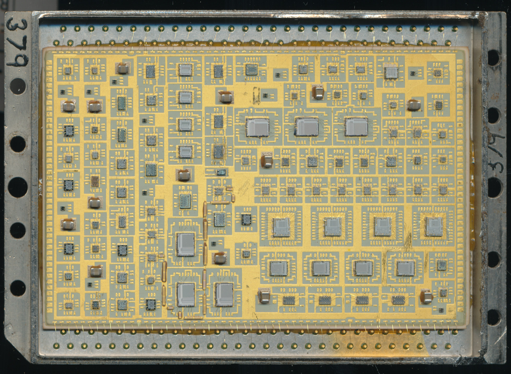
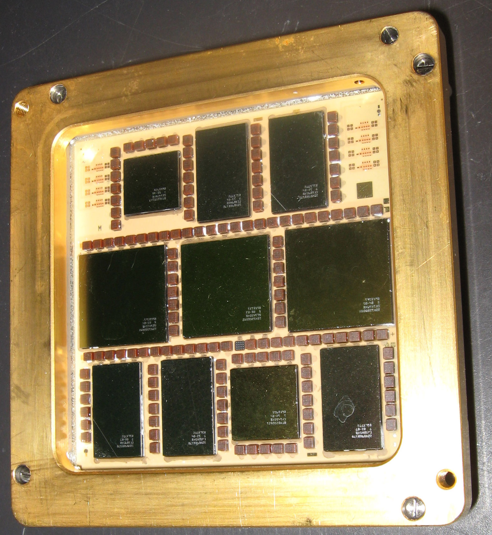
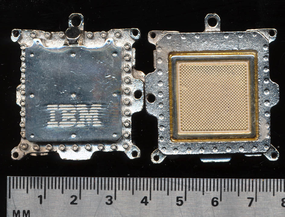
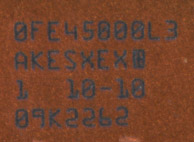
ITT 80063SM-A-919797 – AN/ALQ-136(V)I Processor. The 2901B’s are the 4 larger dies in a row, middle right.

Military computing applications require many custom designs, as they are very mission specific.  A great example is this ITT hybrid processor.  It was designed and used for the AN/ALQ-136(V)1 CMS (CounterMeasures System) for the AH-1F Cobra Attack helicopter.  Two of these hybrids are used in the system, one for the Mod Recovery board, and one for the SLO processor board.  These boards are used to detect hostile pulse RADAR systems, analyze them, and begin jamming based on what type they are.

This requires relatively fast processing, and a generally custom design.  Today a modern DSP processor could handle this task without issue.  However in the early 80’s (the AN/ALQ-136 debuted in 1982) DSP processors were in their infancy.  In 1982 a fast custom processor needed to be built with bit-slice elements.  In this case the very versatile AMD 2901 was used.  The ITT hybrid integrates 4 AMD AM2901B processor dies, as well as associated memory and interfacing elements.  The single package contains almost 100 dies, and many discrete components.  It is built on a ceramic substrate with gold traces, and sealed in a metal package.  This is required to protect the digital components of the system from electronic interference, whether from external sources, or from the helicopters own RADAR systems.  The AN/ALQ-136 is designed to prevent the Cobra from being successfully targeted by RADAR guided missiles, failure means a strong possibility that the helicopter gets hit, not something its crew would like to deal with.

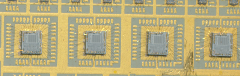
4x AMD AM2901B Dies.

The 4 AMD 2901Bs run at 16MHz (50% faster then the original 2901s) and are made with ECL; together they provide 16-bit processing of the incoming RADAR signals. The SLO (Side Lobe Opposition) and MOD Recovery (Modulation Recovery) are used to determine the exact type of the enemy RADAR.  Each RADAR has a distinct characteristic that the CMS can match and respond to.  The CMS is programmed to respond to the radar signals of the most critical threat weapon systems anticipated to be encoun

Israeli AH-1F Cobras – Now Retired/Transferred to Jordan.

tered in the hostile environment.  These signatures are stored in the hybrids ROMs as well as the desired response to them.  Updates likely remain replacing these hybrids with updated versions.  New countermeasures systems (such as the 136’s replacement, the AN/ALQ-211) are more easily upgradeable to new threats.

The AH-1F Cobra continues to fly with the air forces of several countries around the world, notably Pakistan, Jordan, and Turkey.  The United States Forest Service also operates 25 AH-1F Cobras for wildland fire use, but it is rather unlikely that the countermeasures on these are operable, let alone needed.

September 6th, 2015 ~ by admin

The Electronika MK1 red3 PDP-11 Chipset and Tetris

Soviet Electronika MK1red3 - F-11 Clone and implementation of PDP-11

Soviet Electronika MK1red3 – F-11 Clone and implementation of PDP-11

The DEC F-11 ‘Fonz’ implementation of the PDP-11 was released in 1979 and was DEC’s second ‘LSI’ implementation of the PDP.  Like its predecessor it was a multi-chip implementation, consisting at its root of a data chip (DC302) and 1-9 control chips (DC303).  The DC303 control chips were essentially a large ROM/PLA with a few extra features added for interrupts and sequencing.  They formed the microcoded instruction set that drove the 16-bit ALU and registers of the DC302.  This is why more then one were supported.  Expanding the instruction set was as ‘simple’ as adding more DC303 chips with these instructions encoded.  The basic LSI11/23 came with one 303 and one 302.  A second IC could be added to support floating point, which included a pair of DC303 chips implementing the floating point instructions.  A MMU (DC304) was also supported, and required when using the FP option.

DEC 570000101A1 F11 Floating Point Option with 2x 303E Control chips

DEC 570000101A1 F11 Floating Point Option with 2x 303E Control chips

The Soviets also widely adopted the PDP-11 architecture.  Likely because it was designed to be rather hardware independent.  It could be implemented in many different ways, which meant the Soviets could adopt/implement it on their own.  Electronika was part of the Soviet industrial complex in Voronezh, Russia making many different IC’s, but also was tasked with making consumer devices (computers and calculators etc, that were in very short supply.  The Electronika 60 was one of the first PDP-11 computers they made, and it implemented a copy of the DEC Fonz processor.  Electronika combined the standard chipset, and FPU onto a single large MCM with all 4 IC’s (the MMU remained separate) called the MK1 red1 (and later the MK1 red3)

Tetris Electronika 60 - Text Only

Tetris Electronika 60 – Text Only

KH1811VM1 = DC302 – 21-15541 Data Chip (16-bit ALU etc)
KH1811VU1 = DC303 – 23-001C7 standard instruction set
KH1811VU2 = DC303 – 23-002C7 FP instruction set Part 1
KH1811VU3 = DC303 – 23-003C7 FP instruction set Part 2

It was on this chipset, on a Soviet Electronika 60 that Alexey Pajitnov wrote the very first version of the still famous game of Tetris back in 1984.  A game that was very popular, and very widely copied in the West, even to this day.  (the copying of technology most certainly went both ways)

Tags:
, , ,

Posted in:
CPU of the Day

August 10th, 2014 ~ by admin

An Interesting Fujitsu MCM Pentium Module

Fujitsu MRN-3545 (100) 100MHz Pentium with no L2 Cache

Fujitsu MRN-3545 (100)
100MHz Pentium with no L2 Cache

We have seen Fujitsu MCM Pentiums before.  120MHz, 133MHz 150MHz and MMX ones.  One is pictured in the article on the MicroModule Systems Gemini here.  The 100MHz module is similar, though it is missing the L2 cache tag RAM (256 kbit chip on the top of the package) as well as the 2 cache RAM chips normally installed on the backside of the module.  It would appear that Fujitsu offered these modules with the cache being optional.  There was a 133MHz version (MRN-3548) with cache, and one (MRN-3549) without cache.

These processors were typically used in environmentally challenging environments.  Panasonic famously used them in their ToughBook CF25, the beginning of a line of highly durable laptop in 1996.  Some of these applications were sealed environments, they did not have vents, or active cooling.  This obviously  makes cooling a challenge.  Removing the L2 cache, while causing a significant hit in performance, would alleviate some of the heat generation.

We consider L2 cache to be essential, but many applications do not require it.  Intel infamously removed the L2 Cache completely from the first Celeron processors and while they worked, they were not particularly competitive performance wise.  When competing against wind, rain dirt, and droppage? L2 cache may not be so important

Posted in:
CPU of the Day

March 11th, 2014 ~ by admin

IBM z800 MCM Mainframe Processor

IBM z800 MCM

IBM z800 MCM

Mainframes are the workhorses of the computing industry.  They process transactions for about every industry, and handle the brunt of the economy.  Their MTBF (Mean Time Between Failures) is measured in decades (typically 20-50 years).  A comparison to a home computer is hard to make, they are in an entirely different league, playing an entirely different game.

Data Intense vs. CPU Intense

Mainframe processors such as these work in what is referred to as ‘Data Intensive’ computing environments.  This is different from multi-cored processing that focuses on ‘CPU Intensive’ computing.  CPU intense has a relatively small data set, but most perform a lot of work on that set of data, or do the same instruction on a set of data (such as graphics).  CPU Intense processing can often be sped up with the addition of more processing cores.  Data Intense processing does not see as much benefit from adding cores.  Its biggest bottleneck is accessing the data, thus the System z tends to have VERY large caches, and very high bandwidth memory.  They typically operate on transactional type data, where the processing has to operate in a certain order (A has to be done before B which has to finish before C etc).

IBM was one of the first, and continues to be one of the largest suppliers of such systems.  Starting with the System/360 introduced in 1964 to the zSeries today.  The zSeries was first launched in 2000 with the z900, a significant upgrade from the System/390.  Data addressing was moved to 64-bits (from 31 bits) yet backwards compatibility (all the way back to the 360) is maintained.  The z900 ran at 775MHz and was built with a 35 die MCM containing 20 Processing Units (PUs) and 32MB of L2 Cache.

Read More »

Tags:
,

Posted in:
CPU of the Day

February 18th, 2014 ~ by admin

CPU of the Day: IBM POWER5+ QCM

IBM POWER5+ QCM - 4 dies, 8 cores, and 72MB of L3 Cache

IBM POWER5+ QCM – 4 dies, 8 cores, and 72MB of L3 Cache

When the POWER5 processor was released in 2004 it was made in two versions, a DCM (Dual Chip Module) containing a POWER5 die and its 36MB L3 cache die, as well as a MCM containing 4 POWER5 die and 4 L3 cache dies totaling 144MB.  The POWER5 is a dual core processor, thus the DCM was a dual core, and the MCM an 8 core processor.  The POWER5 contains 276 million transistors and was made on a 130nm CMOS9S process.

In 2005 IBM shrank the POWER5 onto a 90nm CMOS10S manufacturing process resulting in the POWER5+.  This allowed speeds to increase to 2.3GHz from the previous max of 1.9GHz.  The main benefit from the process shrink was less power draw, and thus less heat.  This allowed IBM to make the POWER5+ in a QCM (Quad Chip Module) as well as the previous form factors.  The QCM ran at up to 1.8GHz and contained a pair of POWER5+ dies and 72MB of L3 Cache.

The POWER5+ was more then a die shrink, IBM reworked much of the POWER5 to improve performance, adding new floating point instructions, doubling the TLB size, improved SMP support, and an enhanced memory controller to mention just a few.

The result? A much improved processor and a very fine looking QCM.

Tags:
, ,

Posted in:
CPU of the Day

August 8th, 2013 ~ by admin

How To: Disassembling an IBM POWER4 MCM

The  IBM POWER4 was released in 2001.  It was a 1.1-1.9GHz dual core processor widely used in IBM’s server line including the RS/6000 and AS/400.  It can be commonly found as a single chip dual core, but also as a large MCM containing 4 POWER4 dies. These MCMs include a very large and heavy aluminium heatsink attached to a solid copper housing.  The complete unit weighs in at a hefty 3kg.  The heatsink and housing can be removed revealing a 230 gram MCM (with its small heat spreaders).

IBM POWR4 MCM disassembly

To disassemble one of these you will need a variety of tools.  A 4 mm socket, hex bits (2.5, 3 and 4mm), T8 torx bit , a medium flat tip screw driver, gloves and a good heat source (I use a propane torch)

Remove the Interposer and screws

First remove the 4 T8 torx screws that hold the interposer to the module.  It gets in the way and can melt easily.  Also remove the 8 3mm screws around the perimeter.  These hold the aluminium heatsink to the copper housing.

Read More »

Tags:
, ,

Posted in:
How To

March 13th, 2013 ~ by admin

IBM 3081 TCM Miniature Pendant

IBM 3081 TCM Pendant

IBM 3081 TCM Pendant

A few times I get things that are not processors but are memorabilia and are pretty special nonetheless.  Today these nice IBM pendants came in.  They are very small, measuring barely 37mm square but they weigh an impressive 60 grams.  They are a near perfect miniature version of a not so miniature IBM TCM (Thermal conduction module).  The 3081 TCM contained the cooling, and a very large MCM used in the 308x mainframe series (made from 1980-1987).  Each MCM contained up to 133 dies on a very large ceramic substrate with up to 16,000 contacts for the dies.  They were capable of speeds of up to 38MHz.  Each TCM was liquid cooled and dissipated around 300 watts of heat. A typical 308x system had 2 dozen of these.

A similar IBM MCM can be seen here: (a 9121 processor)

Tags:
,

Posted in:
Just For Fun

February 7th, 2013 ~ by admin

CPU of the Day: Unknown IBM MCM – Any ideas?

IBM MCM

Click for much larger

Every now and then I will get a chip in that I cannot ID.  This is a particularly perplexing one.  It looks like it should be something fairly well known, but I cannot determine what.  By the dates its a 2005 vintage IBM, MCM, on a fairly large ceramic package with 1077 lands.  It contains a pair of Infineon HYB39S256160DT-7 256Mbit (4Mbitx16bit) DRAMs which are 7ns 143MHz max, commonly used on PC133 SDRAM.   That works out to 64MB.  Also on the package is a IBM0436A8ACLAB 8Mbit (256Kx36) 4.5ns (222MHz) 1Mbyte SRAM.

IBM MCM die

IBM MCM die

Markings on the die are:
0FE45000L3
AKESXEX0
1 10-10
09K2262


If you have any ideas what it is, or what it may be, post a comment.  I may just give you one.  These came in with a lot of HP PA-RISC processors, so perhaps related?

UPDATE (10/20/2016): Mystery solved. These are processors from a Cadence Palladium emulator system. Read more about them here

Tags:
,

Posted in:
CPU of the Day

December 3rd, 2012 ~ by admin

GPU of the Day: SGI GE7 Geometry Engine

SGI Extreme 4GE7MCM 256 MFLOPS 320,000 Gates

At 2.6oz (75 grams) and 2.25 inches square (6cm) the SGI 4GE7MCM is a beast of a graphics chip.  More properly called a Geometry Engine was, the GE7 was responsible for all the graphics processing in SGI Indigo2 workstations.  The Indigo2 Extreme graphics option consisted of a pair of these MCMs (Multi-Chip-Module).  Each one contains 4 GE7 Geometry Engines providing 32MFLOPS of performance each.  Each GE7 consists of a custom 80,000 gate array from LSI (for a total of 320,000 gates and 128MFLOPS per MCM).  This performance level was, ironically, better then the main system CPU (35MFLOPs for the 200MHz R4400 option).

Each of the black ‘caps’ on the chip covers a single GE7 Engine.  A similar design was used for the XZ Graphics system that had only 4 total GE7 cores.  This was either implemented with 2 of the large MCMs that had only 2 GE7s in them (same package however) that were marked 2GE7MCM, or, later, a single surface mount MCM containing 4 GE7 engines.  All were manufactured by LSI.  In total the Extreme Graphics subsystem had no less then 31 custom gate arrays from LSI for a total of over 1.2 million gates.   At an average of 2 transistors per gate that works out to around 2.5 million transistors, a considerable amount for a graphics system in 1993.  Today’s graphics chips pack in transistors numbering in the billions, the Geforce GTX 680 has a total of 3.54 billion transistors, and performance measured in TFLOPS, again for the GTX 680, 3.09TFLOPS.  Today’s graphics chips cannot, however, compete with the magnificent looks of the GE7’s giant MCM package.

Sources:
Indigo2 Product Guide (PDF)
Indigo2 Technical Report 


Tags:
, ,

Posted in:
GPU

September 21st, 2012 ~ by admin

CPU of the Day: MicroModule Systems Pentium Gemini

MicroModule Systems GV1-D0-3S-60-120A 120MHz (top side)

MicroModule Systems (MMS) began operations in 1992, following the completion of an agreement to acquire the assets and license rights to the technology of Digital Equipment Corporation’s MCM (Multi-chip Module) engineering and manufacturing business in Cupertino, California. The MicroModule Systems vision was to lead the next wave of electronic integration technology. Previous waves have been: discrete components (1950s), integrated circuits (1960s), large-scale integration (1980s), and system on a chip (mid 1990s).

The MMS Gemini was a module, that includes the National Semiconductor chipset die (x2) , a P54CSLM Pentium die, tag RAM, and cache RAM (128Kx2) as well as an LM75A temperature sensor for thermal management.   MMS used Intel D0 revision P54 processors (with the exception of some early C0 die), a stepping Intel never packaged themselves (it was solely used for the ‘known good die’ program).  When Intel discontinued selling fully tested dies, MMS had no way to build the Gemini and later MMX modules, so in 1998 went out of business. The Gemini was used in many mobile, and rugged PC applications such as the Motorola MW520 Computer used in many police cars.

MMS also produced MCM modules for ROSS, used to make the HyperSPARC processor as well as the Intel Pentium Pro 1MB MCM.   For a company that was only in existence for 6 years, their impact was tremendous. MMS was not alone in their production of Intel Pentium Processor modules…

Fujitsu also made modules using Intel dies.  These were again used in rugged PC applications, laptops, and industrial computers.

Fujitsu MRN-3546 120MHz

Fujitsu made 100, 120, 133, and MMX processors on a MCM type package where the individual components are bonded/soldered to a ceramic substrate (rather then the PC Board)

Tags:
,

Posted in:
CPU of the Day