September 2nd, 2023 ~ by admin

SPARCs in Space: The Cobham UT700 Leon3FT Processor

UAE Mars Hope Mission – IR Imager powered by LEON3FT

In the 1990s the ESA began a project to develop their own, open source, easily usable processor for space applications.  Before this the ESA had used mainly MIL-STD-1750A processors, both American made ones, or direct copies their of, such as the Dynex MAS281, a clone of the McDonnel Douglas MDC281.  The ESA explored many different architectures, including the Motorola MC88K RISC process, the MIPS RISC processor, and AMD 29K RISC processor the SPARC, and somewhat oddly, even the National Semiconductor NS32k series processors (which at the time were fairly powerful and used a fair amount in embedded apps).  The SPARC came out of this as the winner.

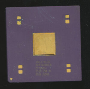
Cypress CY7C601 SPARC Processor. The basis for the ERC32

At the time the SPARC was a pretty widely used processor, and was being developed by multiple companies.  It was defined as an architecture, and various companies could implement it how they saw fit, in various technologies.  This is very much how the 1750A architecture was made to be as well.  Considering this, the only two really viable architectures that wouldn’t (at that time) have been a sole source item, were the MIPS and the SPARC, both were used and made by many companies, but SPARC it was.

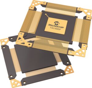
Atmel TSC695 – ERC32 Single Chip SPARC V7 – Still in production

The first implementation was the ERC32 released in 1995, a early SPARC V7 3-chip implementation typically made on a  0.8u process.  These were decent, but took 3 chips, were limited to 20MHz due to memory interface limitations, and were not particularly scalable.  The ERC32 did fly to space, and was used on the ISS as one of the main control computers, as well as 10 other missions including the ESAs ATV resupply vehicles for the ISS.  By 1998 the ERC32 was shrunk to 0.6u allowing it to be integrated onto a single chip (the Atmel TSC695).  This became the standard ESA processor as well as being used by other nations, including China, Israel, India and even NASA.

By the year 2000 the SPARC V7 architecture was rather long in the tooth, having been originally designed back in the 1980’s.  The decision was made to upgrade to SPARC V8.  SPARC V8 added integer multiply/divide instructions, as well as expanded the floating point from 80-bit to 128-bit.  SPARC V8 became the basis for the IEEE 1754-1994 standard for what a 32-bit processor must do.  This was important as it made a very clear definition for software as well, ESA wanted a processor whose support was very well known, and very well defined.  The SPARC V8 implementation became the LEON (for Lion) processor.  These used a 5-stage pipeline (Fetch, Decode, Execute, Memory, Write) and were made on a 0.35u process delivering around 50MIPS at 0.5W. It used around 100,000 gates on a 30mm2 die and was a fully Fault Tolerant design (unlike the ERC32).  It was rated to handle 300Krad of ionizing radiation without upset.
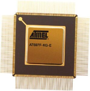
Atmel AT697 LEON2

LEON2 was a fairly similar deign, it moved the MUL/DIV instructions into hardware (instead of emulating them on LEON1) and reduced the feature size down to 0.18u.  It also added many on chip peripherals, such as a PC133 SDRAM controller (with Error detection/Correction) as well as a AMBA bus.  It took around 0.6W at 100MIPS though some implementation saw speeds of up to 120MIPS at 0.3W).  LEON2 saw use on many missions, including the camera controller for the Venus Express mission and the BepiColombo mission to Mercury. LEON2 was designed as a single function processor, but in the real world was often being used as a SoC (System on a Chip).

This led to the development of the LEON3 in 2004.  It was originally made on a slightly LARGER process of 0.20u.  It ran at around 150MIPS at 0.4W.  Its biggest upgrades were moving from a 5-stage pipeline to a 7–stage pipeline (Fetch, Decode, Register Access, Execute, Memory, Exception, Write) as well as supporting multiprocessing.  In realization of the actual use cases the LEON processors were seeing (as SoCs rather then as single processors) the LEON3 added a large array of peripherals.  This included Spacewire, MIL-STD-1553  interfaces, DDR RAM controllers, USB controllers, 1G Ethernet MAC, and much more.  All stuff that originally had to be added on to previous systems was now on chip.

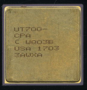
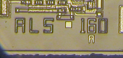
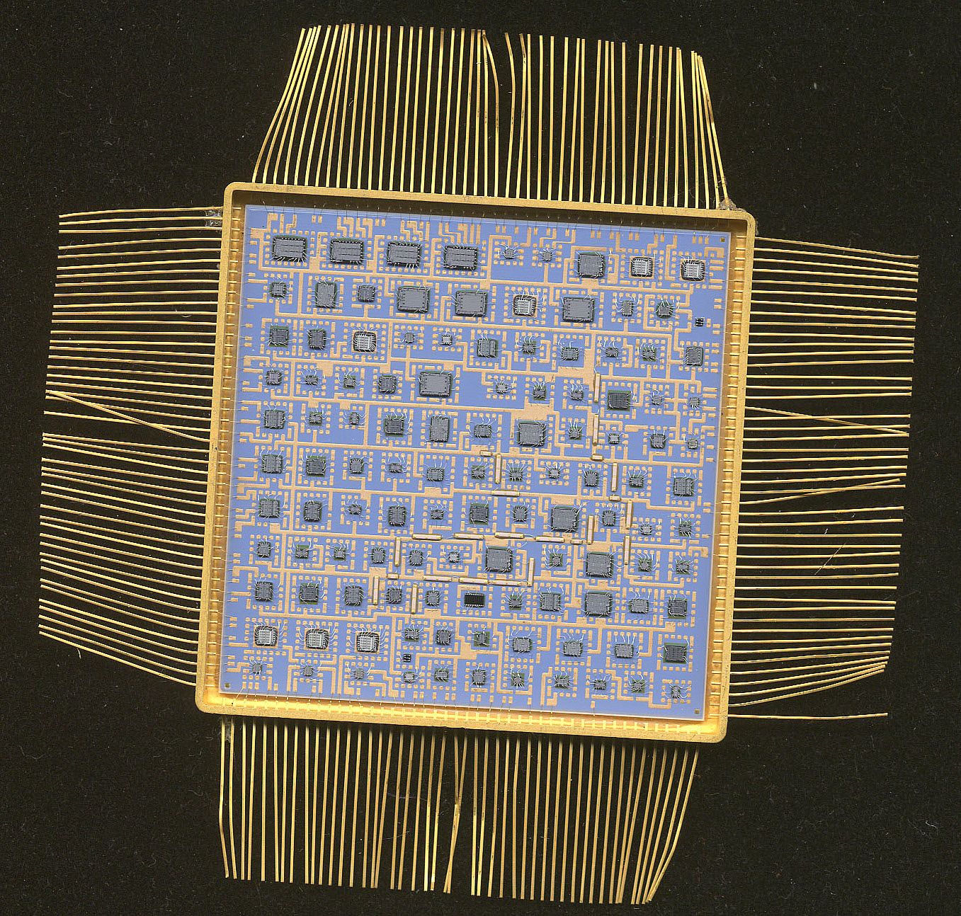
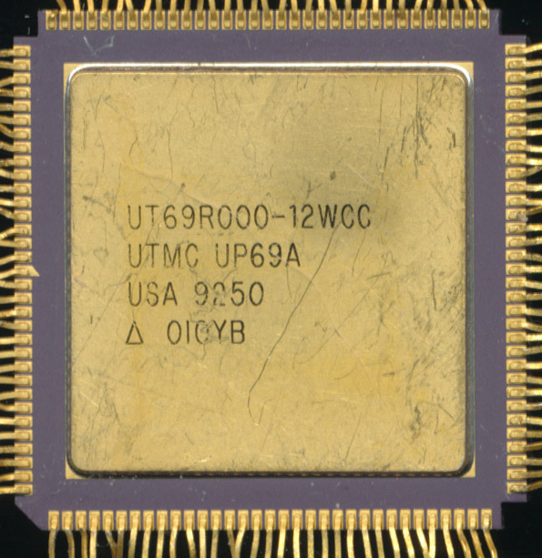
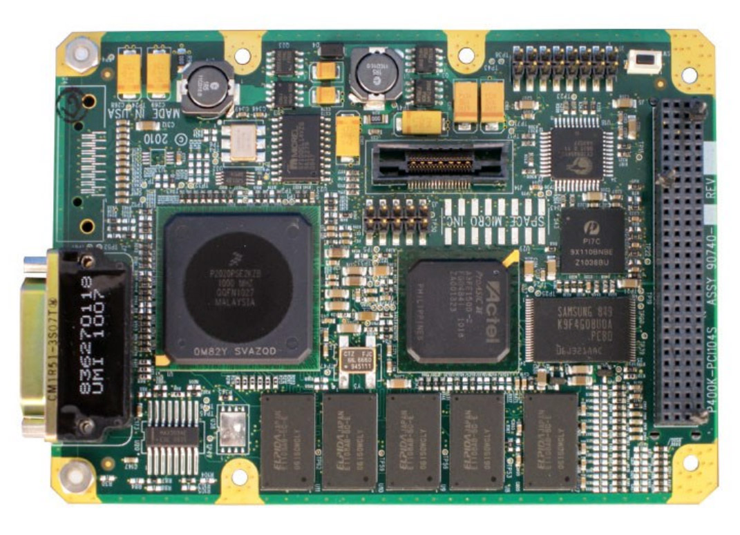
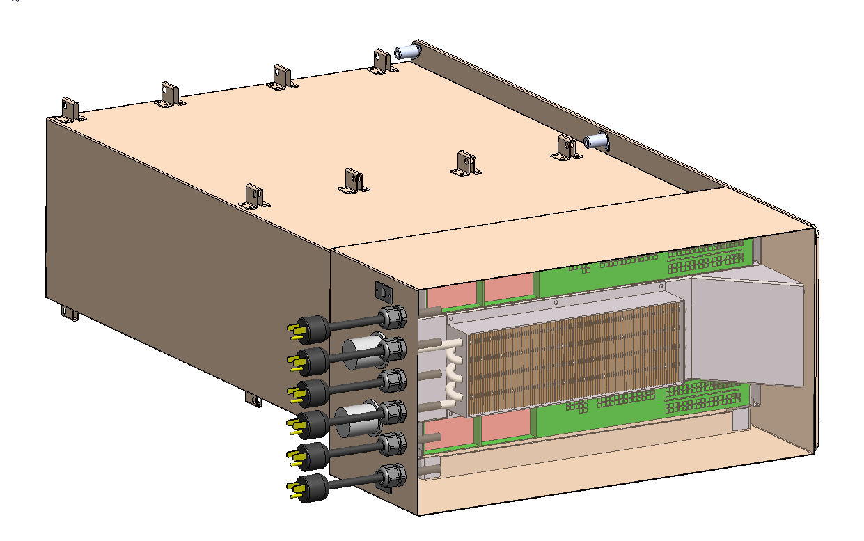
Cobham UT700 Fault Tolerant SPARC V8 LEON3FT

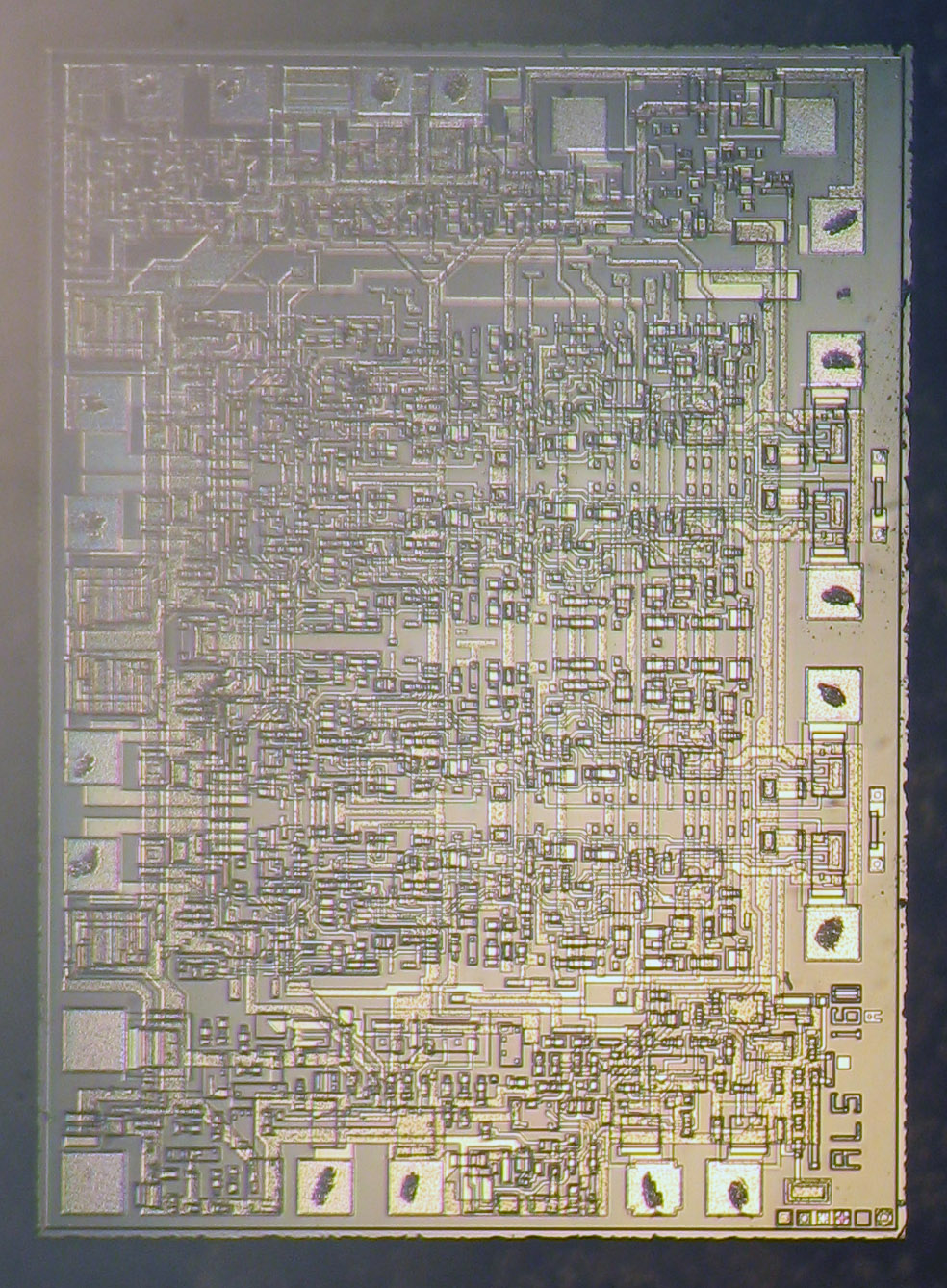
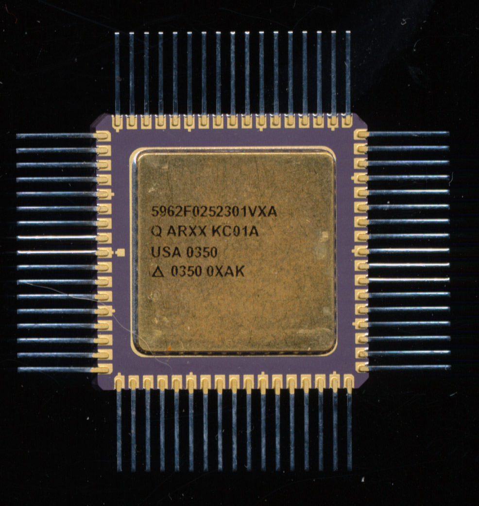
The entire design was good for 400MHz on a 0.13u process and used around 25,000 gates.  Like the LEONs before it, the LEON3 was designed as a synthesizable device.  You could implement the entire core in your on ASIC or FPGA, or buy an FPGA off the shelf already programmed as one (Aeroflex offers this option). You could also buy ready made processors implementing it, much like any other CPU.  Cobham (now known as CAES Cobham Advanced Electronic Solutions) offers the UT700.  The UT700 is a 166MHz processor implementing the full LEON3FT design.  The ‘FT’ stands for Fault Tolerant, and adds a lot of error checking and correcting features on top of the base LEON3 design.  Every bit of RAM on chip, from registers, to cache has error detection and correction.  The UT700 includes 16K of Instruction and Data cache on chip as well as all the usual memory controllers and communication interfaces of the LEON3.  It runs at 1.2-1.8V and and max performance dissipates 4W.

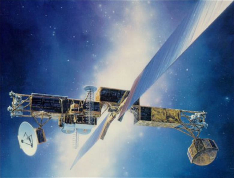
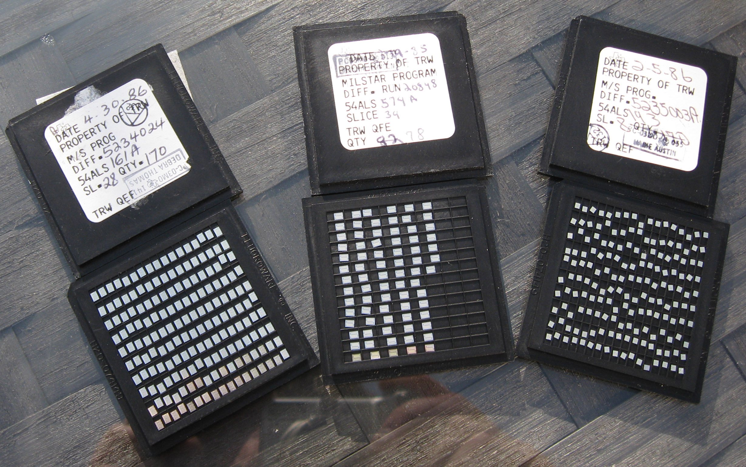
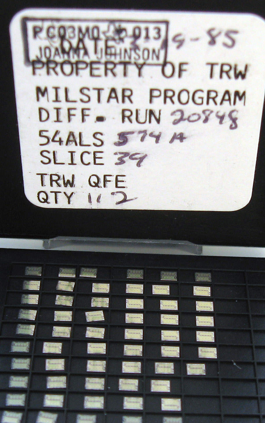
The LEON3FT powers the European Galileo navigation satellites, and many others, including the French Spot-6 Earth Observation craft.  They also power each of the Iridium-NEXT communications satellites that began launching in 2017


Posted in:
CPU of the Day

January 2nd, 2020 ~ by admin

Chips in Space: Making MILSTAR

Milstar Satellite

Back in the late 1970’s having a survivable space based strategic communications network became a priority for the US Military.  Several ideas were proposed, with many lofty goals for capabilities that at the time were not technologically feasible.  By 1983 the program had been narrowed to a highly survivable network of 10 satellites that could provide LDR (Low Data Rate) strategic communications in a wartime environment.  The program became known as MILSTAR (Military, Strategic, Tactical and Relay) and in 1983 President Reagan declared it a National Priority, meaning it would enjoy a fair amount of freedom in funding, lots and lots of funding.  RCA Astro Electronics was the prime contractor for the Milstar program, but during the development process was sold to GE Aerospace, then Martin Marietta, which became Lockheed Martin before the 3rd satellite was launched.  The first satellite was suppose to be ready for launch in 1987, but changing requirements delayed that by 7 years.

Milstar Program 5400 series TTL dies

The first satellite was delivered in 1993 and launched in February of 1994.  A second was launched in 1995 and these became Milstar-1. A third launch failed, which would have carried a hybrid satellite that added a Medium Data Rate (MDR system).  Three Block II satellites were launched in 2001-2003 which included the MDR system, bringing the constellation up to 5.  This provided 24/7 coverage between the 65 degree N/S latitudes, leaving the poles uncovered.

TI 54ALS161A

The LDR payload was subcontracted to TRW (which became Northrup Grumman) and consisted of 192 channels capable of data rates of a blazing 75 – 2400 baud.  These were designed for sending tasking orders to various strategic Air Force assets, nothing high bandwidth, even so many such orders could take several minutes to send.  Each satellite also had two 60GHz cross links, used to communicate with the other Milstar sats in the constellation.  The LDR (and later MDR) payloads were frequency hopping spread spectrum radio system with jam resistant technology.  The later MDR system was able to detect and effectively null jamming attempts.

The LDR system was built out of 630 LSI circuits, most of which were contained in hybrid multi layer MCM packages.  These LSIs were a mix of custom designs by TRW and off the shelf TTL parts.  Most of the TTL parts were sourced from TI and were ALS family devices (Advanced Low Power Schottky), the fastest/lowest power available.  TI began supplying such TTL (as bare dies for integration into MCMs) in the mid-1980’s.  These dies had to be of the highest quality, and traceable to the exact slice of the

Traceability Markings

exact wafer they came from. They were supplied in trays, marked with the date, diffusion run (a serial number for the process and wafer that made them) and the slice of that wafer, then stamped with the name/ID of the TI quality control person who verified them.

These TTL circuits are relatively simple the ones pictures are:
54ALS574A Octal D Edge Triggered Flip flop (used as a buffer usually)
54ALS193 Synchronous 4-Bit Up/Down Binary Counters With Dual Clock
54ALS161A Asynchronous 4-Bit Binary Counters

ALS160-161

Looking at the dies of these small TTL circuits is quite interesting.  The 54ALS161A marking on the die appears to be on top of the a ‘160A marking.  TI didn’t make a mistake here, its just that the the 160 and 161 are essentially the same device.  The 161 is a binary counter, while the 160 was configured as a decade counter.  This only required one mask layer change to make it either one.

ALS573 and ALS574 die

Similarly with the 54ALS574, which shares a die with the more basic ‘573 D type transparent Latch.  This was pretty common with TTL (if you look at a list of the different 7400 series TTL you will notice many are very similar with but a minor change between two chips).  It is of course the same with CPUs, with one die being able to be used for multiple core counts, PCI0E lanes, cache sizes etc.

Together with others they perform all the function of a high reliability communications systems, so failure was not an option.  TI supplied thousands upon thousands of dies for characterization and testing.  The satellites were designed for a 10 year lifetime (it was hoped by them

Milstar Hybrid MCM Command Decoder (picture courtesy of The Smithsonian)

something better would be ready, no doubt creating another nice contract, but alas, as many things are, a follow on didn’t come along until just recently (the AEHF satellites).  This left the Milstar constellation to perform a critical role well past its design life, which it did and continues to do.  Even the original Milstar 1 satellite, launched in 1994 with 54ALS series TTL from the 1980s is still working, 25 years later, a testament to TRW and RCA Astro’s design.  Perhaps the only thing that will limit them will be the available fuel for their on-orbit Attitude Control Systems.

While not necessarily a CPU in itself these little dies worked together to get the job down.  I never could find any of the actual design, but it wouldn’t surprise me if the satellites ran AMD 2901 based systems, common at the time or a custom design based on ‘181 series 4-bit ALUs.  finding bare dies is always interesting, to be able to see into whats inside a computer chip, but to find ones that were made for a very specific purpose is even more interesting.  The Milstar Program cost around $22 Billion over its life time, so one must wonder how much each of these dies cost TRW, or the US Taxpayer?

Tags:
, ,

Posted in:
CPU of the Day

March 1st, 2019 ~ by admin

CPU of the Day: UTMC UT69R000: The RISC with a Trick

UTMC UT69R000-12WCC 12MHz 16-bit RISC -1992

We have previously covered several MIL-STD-1750A compatible processors as well as the history and design of them.  As a reminder the 1750A standard is an Instruction Set Architecture, specifying exactly what instructions the processor must support, and how it should process interrupts etc.  It is agnostic, meaning it doesn’t care. how that ISA is implemented, a designers can implement the design in CMOS, NMOS, Bipolar, or anything else needed to meet the physical needs, as long as it can process 1750A instructions.

Today we are going to look at the result of that by looking at a processor that ISN’T a 1750A design.  That processor is a 16-bit RISC processor originally made by UTMC (United Technologies Microelectronics Center).  UTMC was based in Colorado Springs, CO, and originally was formed to bring a semiconductor arm to United Technology, including their acquisition of Mostek, which later was sold to Thomson of France. After selling Mostek, UTMC focussed on the military/high reliability marked, making many ASICs and radhard parts including MIL-STD-1553 bus products and 1750A processors.  The UT69R000 was designed in the late 1980’s for use in military and space applications and is a fairly classic RISC design with 20 16-bit registers, a 32-bit Accumulator, a 64K data space and a 1M address space.  Internally it is built around a 32-bit ALU and can process instructions in 2 clock cycles, resulting in 8MIPS at 16MHz.  The 69R000 is built on a 1.5u twin-well CMOS process that is designed to be radiation hardened (this isn’t your normal PC processor afterall).  In 1998 UTMC sold its microelectronics division to Aeroflex, and today, it is part of the English company Cobham.

UTMC UT1750AR – 1990 RISC based 1750A Emulation

UTMC also made a 1750A processor, known as the UT1750AR, and if you might wonder why the ‘R’ is added at the end.  The ‘R’ denotes that this 1750A has a RISC mode available.  If the M1750 pin is tied high, the processor works as a 1750A processor, tied low, it runs in 16-bit RISC mode.  How is this possible? Because the UT1750AR is a UT69R000 processor internally.  Its the same die inside the package, and the pinout is almost the same (internally it may be but that’s hard to tell).  In order for the UT1750AR to work as a 1750A it needs an 8Kx16 external ROM.  This ROM (supplied by UTMC) includes translations from 1750A instructions to RISC macro-ops, not unlike how modern day processors handle x86.  The processor receives a 1750A instruction, passes it to the ROM for translation, and then processes the result in its native RISC instructions.   There is of course a performance penalty, processing code this way results in 1750A code execution rates of 0.8MIPS at 16MHz, a 90% performance hit over the native RISC.  For comparison sake, the Fairchild F9450 processor, also a 1750A compatible CPU, executes around 1.5MIPS at 20MHz (clock for clock, about 30% faster), and thats in a power hungry Bipolar process, so the RISC translation isn’t terrible for most uses.

NASA Aeronomy of Ice in the Mesosphere – Camera powered by RISC

By today’s standards, even of space based processors, the UT69R000 is a bit underpowered, but it still has found wide use in space applications.  Not as a main processor, but as a support processor, usually supporting equipment that needs to be always on, and always ready.  One of the more famous mission the UT69R000 served on was powering the twin uplink computers for the DAWN asteroid mission (which only this year ended).  It was also used on various instrumentation on the now retired Space Shuttles. The CPU also powered the camera system on the (also retired) Earth Observing-1 Satellite, taking stellar pictures of our planet for 16 years from 2000-2017.  Another user is the NASA AIM satellite that explores clouds at the edge of space, originally designed to last a couple years, its mission which started in 2007 is still going.  The

JAXA/ESA Hinode SOLAR-B Observatory

cameras providing the pretty pictures are powered by the UT69R000.  A JAXA/ESA mission known as SOLAR-B/Hinode is also still flying and running a Sun observing telescope powered by the little RISC processor.

There are many many more missions and uses of the UT69R000, finding them all is a bit tricky, as rarely does a processor like this get any of the press, its almost always the Command/Data Processor, these days things like the BAE RAD750, and LEON SPARC processors, but for many things in space, and on Earth, 16-bits its all the RISC you need.

April 11th, 2018 ~ by admin

PowerPC Processor for TESS Planet Hunter – Updated

TESS Orbiter – Freescale (now NXP) 2010  PowerPC e500

UPDATE: I received a note from a NASA engineer that the final flight DHU was made by SEAKR Engineering rather then Space Micro.  It turns out MIT pursued 2 different DHU systems in the design of TESS.  The Space Micro IPC 7000 was referred to as the DHU and a system by SEAKR (the Athena-3) was selected as the ADHU (Alternate Data Handling Unit).  Apparently MIT wasn’t sure which would be best so essentially characterized both (and most documentation from early on shows the Space Micro system).  In the end however, the SEAKR Athena-3 Single Board computer was selected.

If all goes well, in a few days the NASA TESS (Transiting Exoplanet Survey Satellite) will be launched on a SpaceX Falcon 9 rocket to startits mission to survey a large portion of the sky for possibly Earth-like planets.  TESS’s finds will make great candidates for further study by either Hubble, or JWST (when it finally launches).  While TESS can see transiting planets (the dimming of a star as an exoplanet passes in front of it) it cannot determine much about its composition, or the composition of its atmosphere.  However, having a list of exoplanets to further check out, especially Earth-sized ones, it’s a big help.  TESS was created as part of the NASA Medium Class Explorers Program (MIDEX) which is for mission up to around $200 Million total cost to NASA (not including launch).  TESS itself cost about $75 million (developed in large part by MIT and built by Orbital-ATK on their LEOStar-2 Platform) and the launch services contract was $87 Million with the remainder taken by operations and contingency funding.

Space Micro Proton 400k with Freescale 2020 processor

That makes this one of the least expensive NASA missions, but one that has engendered much more public interest then its cost suggests.  Finding alien worlds captivates people hearts and minds.  So what is at the heart of the TESS orbiter?  Obviously the premier technology is its 4 cameras that will scan the sky, but the computer that powers these is no less interesting.

The 4 cameras are interfaced to a Data Handling Unit (DHU).  Initially the DHU was to be the Space Micro IPC-7000 computer.  The IPC-7000 consists of a TI TMS320C67xx 32-bit DSP and a pair of Xilinx Virtex-7 FPGAS.  They handle all the pre-processing of the imagery collected by the cameras, making it into a format that is easily transmitted back to earth.  The rest of the spacecraft functions (such as actually sending/storing the data and other space craft house-keeping) is handled by a Space Micro Proton 400k SBC.  The Proton 400k is based on a Freescale 2020 1GHz Dual Core PowerPC processor made on a 0.45u process..  Each PowerPC e500v2 core has a 7-stage pipeline with 32K of I-cache and 32K of D-Cache and shares a single 512K L2 Cache.  The computer also containing a pair of 192GB solid state memory boards for buffering imagery data (data is relayed to Earth only once per orbit, so it needs to store data from around 14 days).

Athena-3 SBC – Powered by a 1.067GHz Freescale P2010 Processor

The final flight version of TESS switched to an ADHU made by SEAKR Engineering.  This uses a very similar setup but a bit less powerful processor.  The heart of the ADHU is the Freescale P2010 e500 processor at 1066MHz with 1GB of DDR2 RAM and 1-4GB of Flash.  This is the single core version of the P2020 used in the initial Proton 400k.  The ADHU also includes a RCC5 triple Xilinx Virtex-5 FPGA board to handle additional camera processing functions (and anything else not handled by the P2010 processor).  Solid state storage is a Gen 3 FMC also by SEAKR, containing 3 boards with a total of 192GB of Flash.  The ADHU handled all of the science, processing the raw camera data into useful science data and handling the sending of data to the 100-125MBit/sec Ka-band transmitter.  It also supplies some star reference information used by the MAU (Master Avionics Unit) computer to provide finer attitude control of the satellite.  The MAU is the LeoStar-2 Satellites main computer, and handles all the mechanics of flying the spacecraft outside of the science work done by the ADHU.

Freescale P2020 Processor

In many ways this is a very advanced processor compared to the RAD750 processors we often see on large scale NASA missions.  The Freescale 2020/2010 is not an inherently radiation hardened design, however both Space Micro and SEAKR  implements many radiation mitigating designs in the system design to compensate for this.  It is not as robust as the RAD750 but it is a $75 million earth satellite with a target mission life of 2-years so it doesn’t need to be. The 2020 processor does give TESS tremendous processing power for a scientific satellite, allowing for a lot of pre-processing of the imagery.  This allows TESS to handle much of the grunt work, and send scientists here on Earth only the very best data, in a format that is the most useful to them.


Tags:
,

Posted in:
CPU of the Day

August 17th, 2017 ~ by admin

Intel Broadwell Broadens its Horizons…In Space

SpaceX CRS-12 – Carrying 116lbs of High performance Broadwell computers (image: SpaceX)

Monday’s launch of a SpaceX Falcon 9 rocket carrying a Dragon spacecraft to the space station carried what will be the most powerful computer in orbit.  In a joint project with HPE (HP Enterprise) NASA wants to test how high end computers, with off the shelf parts and construction perform in low Earth orbit.  The computer that will be soon installed is an HP Apollo 40 series (exact model is unclear, probably PC40/SX40).  It consists of 2 1U dual socket systems, running Intel Xeon E5-26xx V4 (Broadwell-EP 14nm) processors and supporting infiniband.  The only modification done was to use liquid cooling vs air cooling as the EXPRESS racks on the ISS are not set up to handle the heat load the computer generates.  The computers run on a standard 110VAC supply, provided by a NASA supplied inverter, which takes the 48VDC power generated by ISS’s solar arrays and converts it to the 110VAC needed by the Apollo computer.

The Broadwell processors are made on a 14nm process, and are some of the latest made by Intel (NASA froze the design in March so they were the fastest available to HPE at that time).  Performance will be just over 1Teraflop, a great increase over the main computers that actually RUN the ISS, which are Intel 80386SX based.  The astronauts themselves use laptops of various pedigrees, mainly Lenovo Core 2 Duo based A61Ps (these are being replaced by HP Zbook 15s powered by Intel 7th Gen Core i5 and i7 processors) , so the Apollo is a great leap up from them as well.

Mockup of HPE Apollo Computers for EXPRESS rack integrations. 2 computers with water cooling system between them.

To test the Apollo, NASA will run an identical system on the ground, performing the same tasks, and compare the outputs.  They want to see how the computers handle the environment in space, with various loads and electrical conditions.  One computer (both on the ground and on the ISS) will be run at maximum performance for the entirety of the experiment, while the other will have its computing/electrical load dynamically varied.

Radiation is usually one of the biggest concerns for space based computers, but on the ISS, radiation levels are not particularly high.  Daily doses experienced by the crewmembers are in the 10-50 millirad range. There are of course periods of higher radiation, either from where the ISS is in orbit, or from space weather.  The water cooling will further shield parts of the computer from radiation (water being a great radiation shield).  The Broadwell-EP processors have around 7.2 billion transistors, increasing the

10-core Broadwell die. Made on 14nm process.

chance that even a small amount of radiation may have an effect.  By running one set of computers at maximum performance, NASA can see these effects quickly.  Does the performance decrease? Does the power draw start spiking? Or is data being lost in the Infiniband networking PCIe card?

Currently experiment data has to be transferred to the ground in raw unprocessed format, as nothing on the ISS can handle the computing need to process it.  If the high performance computing experiment is successful, it can give the astronauts the ability to do processing and analysis of experimental data in orbit,. and transfer only the results to the ground, saving precious bandwidth, and allowing for experiments to be modified, changed, or created in orbit based on the ongoing results.


More Information: 

NASA: HPC COTS Experiment

HPE: The space station gets a new supercomputer

Tags:
,

Posted in:
Processor News

February 26th, 2017 ~ by admin

Aeroflex UT80CRH196KDS – The MCS-196 Goes to Space

Aeroflex 5962F0252301VXA = UT80CRH196KDS
F = 3×10⁵ Rad
01 = Mil Temp (-55C-125C)
V = Class V

The MCS-196 is the second generation of Intel’s MCS-96 family of 16-bit processors.  These are a control oriented processor originally developed between Ford Electronics, and Intel in 1980 as the 8060/8061 and used for over a decade in Ford engine computers.  They include such things as timers, ADC’s, high-speed I/O and PWM outputs.  This makes them well suited for forming the basis of applications requiring control of mechanical components (such as Motors, servos, etc).  The 196KD is a 20MHz CMOS device with 1000 bytes of on die scratch pad SRAM. The UT80CRH196KDS (unqualified/not tested for radiation) is priced at $1895.00 in quantities of 5,000-10,000 pieces (in 2002). Fully qualified ones will of course cost a lot more. The KDS is a drop in replacement for the previous KD version, which only supported doses of 100krads.

This obviously lends itself to automotive applications, hard disk control, printers, and industrial applications.  There is however, another application they have found wide spread use in, spacecraft.  Spacecraft are not all to different from a car in the amount of mechanical systems that must be interfaced to the computer controls.  The difference however, is that unlike your car, spacecraft electronics must work, always.  If a car fails, its an annoyance, if a spacecraft fails, it has the potential to cost millions of dollars, not to mention the loss of a mission.  If that spacecraft happens to be the launch vehicle, a failure can directly result in a loss of life.

Read More »

Posted in:
CPU of the Day

January 28th, 2017 ~ by admin

Stratus: Servers that won’t quit – The 24 year running computer.

Stratus XA/R (courtesy of the Computer History Museum)

Making the rounds this week is the Computer World story of a Stratus Tech. computer at a parts manufacturer in Michigan.  This computer has not had an unscheduled outage in 24-years, which seems rather impressive.  Originally installed in 1993 it has served well.  In 2010 it was awarded for being the longest serving Stratus computer, then being 17 years.  Phil Hogan, who originally installed the computer in 1993, and continues to maintain it to this day said in 2010  “Around Y2K, we thought it might be time to update the hardware, but we just didn’t get around to it”  In other words, if it’s not broke, don’t fix it.

Stratus computers are designed very similar to those used in space.  The two main difference are: 1) No need for radiation tolerant designs, let’s face it, if radiation tolerance becomes an issue in Michigan, there are things of greater importance than the server crashing and 2) hot swappable components.  Nearly everything on a Stratus is hot-swappable.  Straus servers of this type are based on an architecture they refer to as pair and spare.  Each logical processor is actually made from 4 physical CPU’s.  They are arranged in 2 sets of pairs.

Stratus G860 (XA/R) board diagram. Each board has 2 voting i860. (the pair) and each system has 2 boards (the spare).  The XP based systems were similar but had more cache and supported more CPUs.

Each pair executes the exact same code in lock-step.  CPU check logic checks the results from each, and if there is a discrepancy, if one CPU comes up with a different result than the other, the system immediately disables that pair and uses the remaining pair.  Since both pairs are working at the same time there is no fail-over time delay, it’s seamless and instant.  The technician can then pull the mis-behaving processor rack out and replace it, while the system is running.  Memory, power supplies, etc all work in similar fashion.

These systems typically are used in areas where downtime is absolutely unacceptable, banking, credit card processing, and other operations are typical.  The exact server in this case is a Stratus XA/R 10.  This was Stratus’s gap filler.  Since their creation in the early 1980’s their servers had been based on Motorola 68k processors, but in the late 1980’s they decided to move to a RISC architecture and chose HP’s PA-RISC.  There was a small problem with this, it wasn’t ready, so Stratus developed the XA line to fill in the several years gap it would take. The first XA/R systems became available in early 1991 and cost from $145,000 to over $1 million.

Intel A80860XR-33 – 33MHz as used in the XA/R systems. Could be upgraded to an XP.

The XA is based on another RISC processor, the Intel i860XR/XP.  Initial systems were based on 32MHz i860XR processors.  The 860XR has 4K of I-cache and 8K of D-cache and typically ran at 33MHz.  Stratus speed rating may be based on the effective speed after the CPU check logic is applied or they have downclocked it slightly for reliability. XA/R systems were based on the second generation i860XP.  The 860XP ran at 48MHz and had increased cache size (16K/16K) and had some other enhancements as well.  These servers continued to be made until the Continuum Product Line (Using Hewlett Packard “PA-RISC” architecture) was released in March of 1995.

This type of redundancy is largely a thing of the past, at least for commercial systems.  The use of the cloud for server farms made of hundreds, thousands, and often more computers that are transparent to the user has achieved much the same goal, providing one’s connection to the cloud is also redundant.  Mainframes  and supercomputers are designed for fault tolerance, but most of it is now handled in software, rather than pure hardware.

Posted in:
Museum News

November 5th, 2016 ~ by admin

GRAPE-6 Processor: A Gravitational Force of Reckoning

GRAPE-6 Processor - 90MHz

GRAPE-6 Processor – 90MHz -2000

Understanding the movements of the stars has been on mankinds mind probably since we first stared into the sky.  Through the ages we can predict where a star or planet will be in the sky in the next few months, years, even hundreds of years, but to be able to predict the exact orbital details for ALL time is rather more tricky.

This helps understand how planetary systems form, and the conditions that make that possible.  It allows us to see what happens when two massive black holes pass each other by, will the merge? will they orbit? will one go rogue?  These are interactions that take millions of years, and thus we need to calculate the gravitational forces very accurately. This isnt a terribly hard problem for two bodies, and is doable for three with little fuss, but for numbers of bodies greater then that, the calculations grow rapidly, on the order of N2/2.

In the late 1980’s Tokyo University began work on developing a computer to calculate these forces.  Every gravitational force had to be be calculated with its effects on every other body in the system.  These results were then fed to a commodity computer for summation and final results.  This made the Tokyo project a sort of Gravity co-processor, or as they called it a Gravity Pipeline, GRAPE for short.  The GRAPE would do the main calculations and feed its results to another computer.

Read More »

Tags:
,

Posted in:
CPU of the Day

September 13th, 2016 ~ by admin

OSIRIS-REx: Bringing Back Some Bennu

OSIRIS-Rex: RAD750 to Bennu

OSIRIS-Rex: RAD750 to Bennu

The Apollo Group  carbonaceous asteroid Bennu is a potential Earth impactor, with a 0.037% likelihood of hitting earth somewhere between 2169 and 2199.  Bennu is thought to be made of materials left over from the very early beginnings of our solar system, making researching them a very tantalizing proposition.  Rather than wait for the small chance of Bennu delivering a sample to Earth in 150 years the thoughtful folks at NASA decided to just go fetch a bit of Bennu.  Thus is the mission of OSIRIS-REx which was launched a few days ago (Sept 8, 2016) aboard an Atlas V 441 as an $850 Million New Frontiers mission.

Somewhat surprisingly there is scant details about the computer systems that are driving this mission to Bennu.  OSIRIS-REx is based on the design of the Mars Reconnaissance Orbiter (MRO), MAVEN and Juno, and thus is based on the now ubiquitous BAE RAD750 PowerPC processor running the redundant A/B side C&DH computers.  This is the main ‘brain’ of the Lockheed Martin built spacecraft.  Of course the dual RAD750s are far from the only processors on the spacecraft, with communications, attitude control, and instrumentation having their own (at this point unfortunately unknown) processors.

REXIS Electronics: Virtex 5QV - Yellow Blocks are Off the Shelf IP, Green Blocks are custom by the REXIS Team. Powered by a Microblaze SoftCore.

REXIS Electronics: Virtex 5QV – Yellow Blocks are Off the Shelf IP, Green Blocks are custom by the REXIS Team. Powered by a Microblaze SoftCore.

One instrument in particular we do know a fair amount about though.  Regolith X-ray Imaging Spectrometer (REXIS) is a student project from Harvard and MIT. REXIS maps the asteroid by using the Sun as an X-ray source to illuminate Bennu, which absorbs these X-rays and fluoresces its own X-rays based on the chemical composition of the asteroid surface. In addition REXIS also includes the SXM, to monitor the Sun’s X-Rays providing context to what REXIS is detecting as it maps Bennu.  REXIS is based on a Xilinx Virtex-5QV Rad-Hard FPGA.  This allows for a mix of off the shelf IP blocks, and custom logic as well. The 5QV is a CMOS 65nm part designed for use in space.  Its process, and logic design are built such as to minimize any Single Event Upsets (SEU), and other radiation induced errors.  It is not simply a higher tested version of a commercial part, but an entirely different device.   Implemented on this FPGA is a 32-bit RISC softcore processor known as Microblaze.  The Microblaze has ECC caches implemented in the BRAM (Block RAM) of the FPGA itself and runs at 100MHz.

It will take OSIRIS-REx 7 years to get to Bennu, sample its surface, and return its sample to Earth.  By the time it gets back, the RAD750 powering it may not be so ubiquitous, NASA is working on determining what best to replace the RAD750 with in future designs.  Currently several possibilities are being evaluated, including a QuadCore PowerPC by BAE, a QuadCore SPARC (Leon4FT), and a multi-core processor based on the Tilera architecture.  As with consumer electronics, multi-core processors can provide similar benefits in space of hogher performance and more flexible power budgeting all with the added benefit (when design for such) of increased fault tolerance.

July 3rd, 2016 ~ by admin

Juno Joins Jupiter: And Brings Some Computers For The Trip

Juno - RAD750 Powered Mission to Jupiter

Juno – RAD750 Powered Mission to Jupiter

NASA’s Juno mission to Jupiter arrives in just about a day, after a 5 year journey that began in August of 2011 aboard an Atlas V rocket.  The Juno mission is primarily concerned with studying the magnetic fields, particles, and structure of Jupiter.  Finding out how Jupiter works, and what its core is made of are some of Juno’s goals.  None of the experiments need a camera, but NASA decided, in the interest of public outreach and education, that if you are going to spend $1 billion to send a probe to Jupiter, it probably should have a camera.  Energetic particle detectors, Magnetometers, and Auroral Mappers are great for science, but what the public is inspired by is pretty pictures of wild and distant worlds.

Juno is powered by a now familiar computer, the BAE RAD750 PowerPC radiation hardened computer.  It operates at up to 200MHz (about the processing power of a mid 1990’s Apple Computer) and includes 256MB of Flash memory and 128MB of DRAM.  It (and the other electronics) are encased in a 1cm thick titanium radiation vault.  Flying in a polar orbit around Jupiter, Juno will experience intense radiation and magnetic fields.  The probe is expected to encounter radiation levels in the order of 10Mrads+.  The vault limits this to 25krads, within what the electronics can handle.  It should be noted that a dose of 10krads is fatal in most cases.  This intense of radiation will degrade the prober, even with shielding, resulting in a mission life of only 37 orbits (a little over a year) before the probe will be gracefully crashed into Jupiter.

Read More »