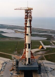
January 19th, 2023 ~ by admin

A history of the EPROM in the Soviet Union

Dov Frohman

In 1971 Intel came out with the first memory that could be not only programmed by the user, but could be erased with UV light and programmed again. This was the 1701 EPROM (quickly revised into the 1702 EPROM and 1702A). It was 2048 bits (256×8), used PMOS, and required three voltage (+5V, +12V and -12V) to operate, and each data line required a strobed -48V pulse for programming.

The 1701 was introduced to the world in the May 10, 1971 issue of Electronics Magazine in an article written by Dov Frohman, the inventor of the EPROM.  Today Intel is more known for, and remembered by their microprocessors, but until the early 1980’s it was EPROM’s that carried the company.  They accounted for the largest share of profits at Intel for over a decade.

K505RR1

Soviet K505RR1 – 1978

Intel 1701 – Unmarked


The first EPROM chip produced in the Soviet Union was the K505RR1, developed by the Kyiv Research Institute of Microdevices and manufactured by the Kvazar factory in Kyiv, Ukraine. The chip is a 2048-bit (256×8) electrically programmable read-only memory with ultraviolet erasure. It is an analogue of the 1702А.
They supported up to 20 (they wore out quite quickly)  overwrite cycles and had a data retention period in on state of not less 5000 hours. This is one of the only EPROM chips manufactured in the flat pack package. NEC made a 2Mbit flat pack EPROM in the 1990s, quite a strange beast.

K573RF1

Analogue of the i2708. The microcircuit is a read-only memory device with a capacity of 8 Kbit (1024х8). Supply voltages of  12v, 5v, -5v. Data Retention period in on state is not less 15000 hours. Number of write cycles at least 100. (a nice improvement over the previous generation)

Microcircuits were manufactured at two factories: Novosibirsk Factory Vostok and Novosibirsk Electrovakuum Factory (NEVZ). The ‘3’ logo is an export version.

NEVZ – 1984


NEVZ military grade version(without letter K + rhombus) -1986

Vostok – 1982


Export – 1986


Export – 1987


On microcircuits with a metal cover, you can see that a part of the conductor connecting this cover and GND pin has been mechanically removed. In electrochemical coating, it’s necessary that all surfaces on which gold is deposited in this case be connected to each other.  But the K573RF1 chip has three power supplies. And minus 5 volts is applied to the die substrate. Part of the conductor has been removed to avoid a possible short circuit.

It’s clearly seen that the die of K573RF1 is divided into two memory blocks.

In the manufacture of dies, it happens that several memory cells turn out to be damaged. The manufacturer blocks access to damaged part of the die by connecting one or two input addresses to ground or a power supply. Either guarantees the operation of only half of the data bus of the microcircuit. K573RF11, K573RF12 have an information capacity of 4 Kbit (512×8) ,  K573RF13, K573RF14- 4 Kbit (1024×4).

Read More »

Posted in:
EPROM of the Day

October 19th, 2022 ~ by admin

Soviet Argon-11S Computers for Space

Saturn-V

The launch by the Soviet Union of the first artificial satellite of the Earth and the first man into space was a real shock for the United States, raising the question in the eyes of the whole world whether the United States is really the leader of world technological progress. Moreover, not only American elites, but also ordinary citizens felt deeply wounded. A month and a half after Gagarin’s flight, US President John F. Kennedy announced the launch of an ambitious lunar space program. On September 12, 1961, Kennedy addressed the nation, calling for a manned mission to the Moon at any cost.

This is actually the first and main reason for the Americans’ success – their lunar mission program became a single “national impulse,” for which no effort or money was spared. At the same time, the Soviet Union accepted the challenge posed by the Americans rather “out of inertia,” as a response to their lunar program. Moreover, by that time the USSR had proved what it wanted, and there was no urgent need to be the first on the Moon anymore. Initially, the Moon landing was not part of the Soviet space program. In the late ’60s and early ’70s it was planned to build a large orbital station and a spacecraft for an expedition to Mars and Venus. Officially, the Soviet lunar program did not begin until 1964.

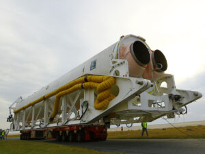
The key point of the lunar mission program was the development of a super-heavy launch vehicle capable of accelerating a craft weighing several tens of tons to the second cosmic velocity (aka escape velocity). In the U.S. NASA began to create a family of rockets known as Saturn. Although unofficially, NASA began to think about the Moon in 1960, even before Kennedy’s speech, and were working on various options for heavy launchers. The name “Saturn V” hints that the launch vehicle was the fifth model in the family. There were other options, even heavier than Saturn V, with some being planned for a Mars mission as well.

The question was who would build it. The chief architect of the Saturn V, Werner von Braun, chose the division of labor. This allowed him to choose the best of the best in the whole industry. He was able to use the most experienced people from each of the companies. For contractors, the decision meant big orders, not a huge order for any one. In the end, the main share was distributed among three companies: Boeing, North American Aviation and Douglas. All in all, more than 20,000 contractors and subcontractors were involved in the production of the rocket.

The first launch of the three-stage Saturn V rocket took place on November 9, 1967 and showed its amazing capabilities. The 3rd stage with the Apollo unmanned spacecraft and the lunar module mass-dimension model with a total mass of 126 tons entered orbit. And thanks to the sixth launch, humanity took a “giant step” toward the first landing of astronauts on the Moon. On July 21, 1969, astronauts Neil Armstrong and Edwin Aldrin made their first ever landfall on the surface of a natural Earth satellite. The Saturn V rocket still amazes today with its grandiosity. With a launch weight of 3,000 tons, it has a height of 110 meters, making it the tallest rocket in the history of world astronautics.
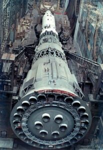
N1 Business end

What about the USSR? In the Soviet Union, work on N1- a superheavy launch vehicle, began back in 1958. As noted above, it was originally created not to provide flights to the Moon, but to build an orbital station, as well as to launch interplanetary expeditionary spacecraft modules into orbit. Later, however, a belated decision was made to include the USSR in the “lunar race” with the delivery of a man to the surface of the Moon. Thus, the N1 rocket program was accelerated. Before determining the final scheme of the launch vehicle, the creators had to evaluate at least 60 different options. They decided on a scheme with spherical tanks for fuel and oxidizer, as well as a load-bearing outer shell, which was supported by a power set and circular placement of the rocket engines in each of the stages.  The First stage alone had 30 engines, which is a plumbing nightmare (as SpaceX is working out with their Starship launch system)

The stages of the N1 rocket were connected to each other by special transition trusses. The rocket complex, which included the launch vehicle H1 and the lunar system to send to the lunar surface with the subsequent return to Earth of a crew of two (the moon landing involved one person) was designated as N1-L3.

The N1 was never static fired, this led to issues being discovered at launch that would have been easier to catch without destruction if it had been

Getting ahead of myself, I will say that none of the launches of the N1 heavy launcher were successful.

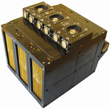
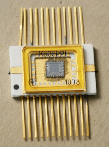
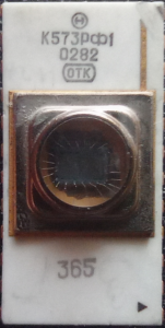
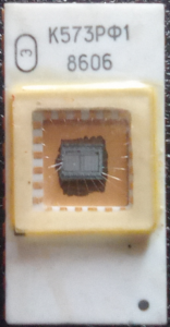
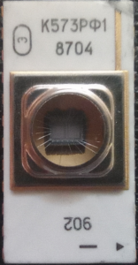
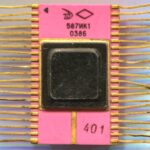
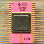
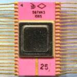
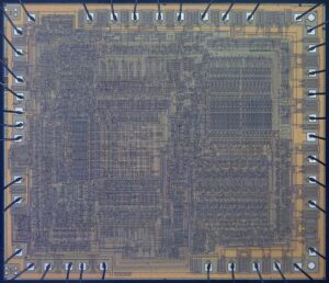
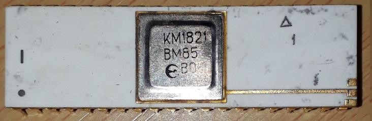
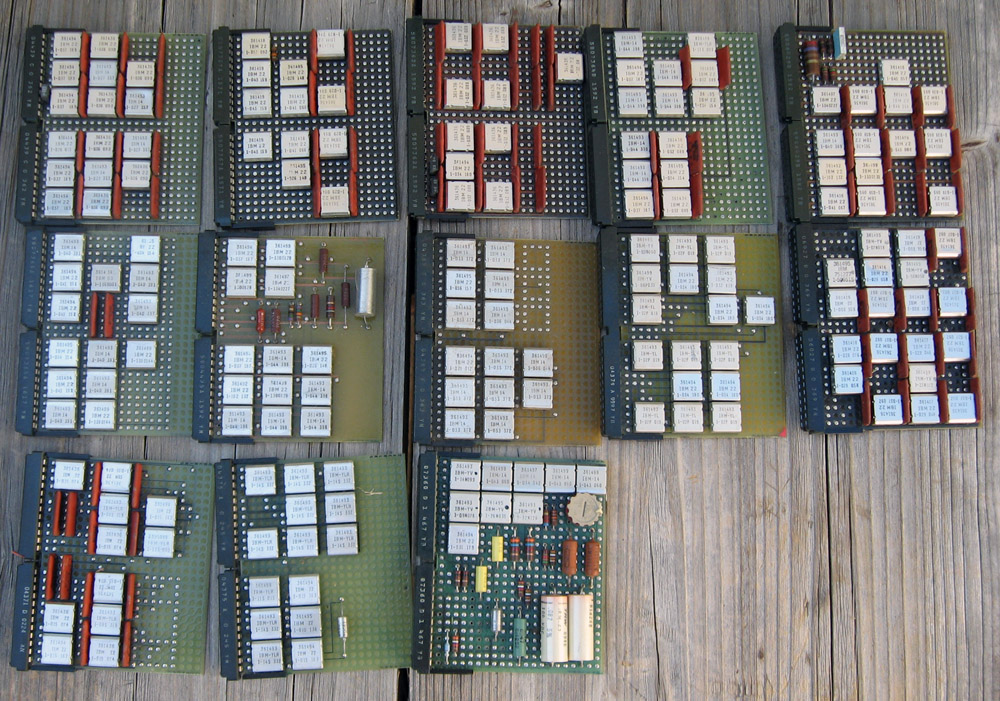
Onboard computer “Argon-11S”.

While the designers were trying to correct the mistakes made in the design of the N1 rocket, the technique of flights to the Moon with a return to Earth after a ballistic flight around the natural satellite of the Earth was being worked out. There have been launches of the Zond spacecraft series using the Proton launch vehicle. These spacecraft were an unmanned version of the two-seater manned spacecraft. All work was carried out in conditions of high secrecy. But now we can say for sure that the Zond-6 and Zond-7 spacecraft were controlled by an onboard digital computer. The Argon-11S.

It consisted of three functionally autonomous computing devices with independent inputs and outputs, interconnected by channels for information exchange and synchronization.


Fixed-point representation. Data bus -14 bit, commands – 17 bit. Number of commands – 15.
Execution time of operations (µs): addition – 30, multiplication – 160.
RAM capacity was 128 14-bit words, ROM capacity – 4096 17-bit words.
Weight 34 kg

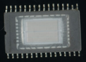
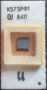
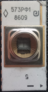
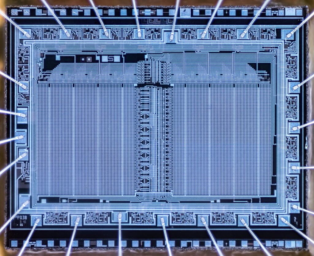
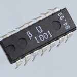
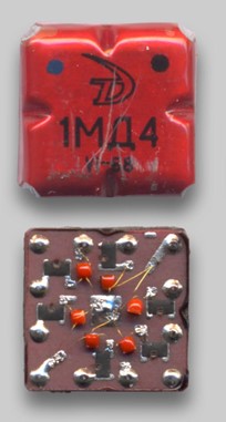
Element base: integrated hybrid microcircuits “Tropa-1”. The microcircuits of small integration degree are made on thick films and form a system of logic elements with direct links (OR, OR – NOT, AND – NOT, etc.). Microcircuits are made in the square metal-polymer case of size 11,6 x 11,6×4 mm, weight of microcircuits is not more than 1,5 g.

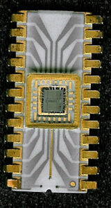
These were very similar to IBM’s SLT architecture for the System/360 mainframes in the USA at that time period as well.

Historically, these were the first integrated circuits developed in the Soviet Union. The active elements were shell-less transistors. The first prototypes of the series were named 1MD1-1MD6, 1MM1-1MM3. Hundreds of logic circuits were mounted on printed circuit boards and bundled together like a book.

Structurally, Argon-11S consisted of three identical functional blocks operating in parallel and independently of each other. The inputs of each block received exactly the same information from many telemetry sensors. On its basis, each block produced more than forty control actions. For the first time in the practice of creating onboard computers, a node redundancy scheme was applied. The final control actions were formed according to the majority principle. That is, if they were the same on two of the three outputs and different on the third, the values generated by the majority were taken as the basis. In fact, Argon- 11S was constantly voting for the most correct control action.

Various IBM System/360 cards showing similar technology at the Soviet Tropa series.

Zond-6 was the ninth launch of a prototype spacecraft. The purpose of the mission was an unmanned flight and photography of the Moon, the return of the lander to Earth with a landing in a given area, as well as practicing the functioning of the manned spacecraft in automatic version. Unfortunately, due to malfunction of the parachute ejection equipment, the vehicle crashed. After the failure of the Zond-6 return to Earth, Zond-7 was launched to the Moon on August 8, 1969. The day after the launch, the spacecraft maneuvered on an intermediate trajectory and obtained color photographs of the Earth. On August 11, the spacecraft flew around the Moon at an altitude of 1,985 km and conducted two sessions of photographs of the Moon and Earth. Zond-7 returned to Earth on August 14.

After a normal dive into the atmosphere, it landed successfully. The photograph taken by Zond-7 is less well-known than the Blue Marble taken by the crew of the Apollo 17 spacecraft, but it is no less beautiful.

This photo ended up on the mail block dedicated to the flights of these spacecraft.

It must be said that not everything was smooth with Zond-7. Prior to this success, there were three high-profile failures. Three rockets (two of them N1 and one Proton) with similar spacecraft exploded on the launch pads.

Despite the fact that none of the N1 rockets managed to complete the launch program, the designers continued to work on it. The next, fifth launch was scheduled for August 1974, but did not take place. In May 1974, the Soviet lunar program was closed, and all work on the N1 ceased. Two rockets ready for launch were destroyed.

Antares 100 series flew 3 times with NK-33 engines, the 4th flight was unsuccessful and resulted in a large explosion.

Only 150 engines of the NK-33 (the successor of the original NK-15 for the first N1s)  type manufactured for various stages of the rocket were saved from the N1. These engines had a chance to fly already in America. They were used in the first stage of the Antares 100 series launch vehicle of the Orbital Sciences Corporation (Now Northrup via Orbital ATK).  They also continue to be used on the Russian Soyuz-2.1v rocket, with the latest launch in April of 2022, still using engines built in the 1960’s, albeit with more modern electronics.
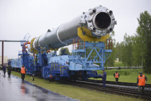
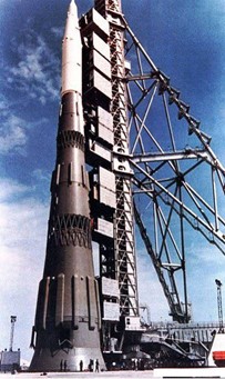
Soyuz-2.1v

Having lost the “Moon Race”, the Soviet Union concentrated its efforts on other projects that had a less prestigious, but no less important role in space exploration – orbital stations, as well as a fairly successful science campaign exploring Venus.  Hopefully in the next few years we will be able to see another truly massive rocket, with 33 engines on the first stage, launch, heading to the Moon, Mars, and beyond
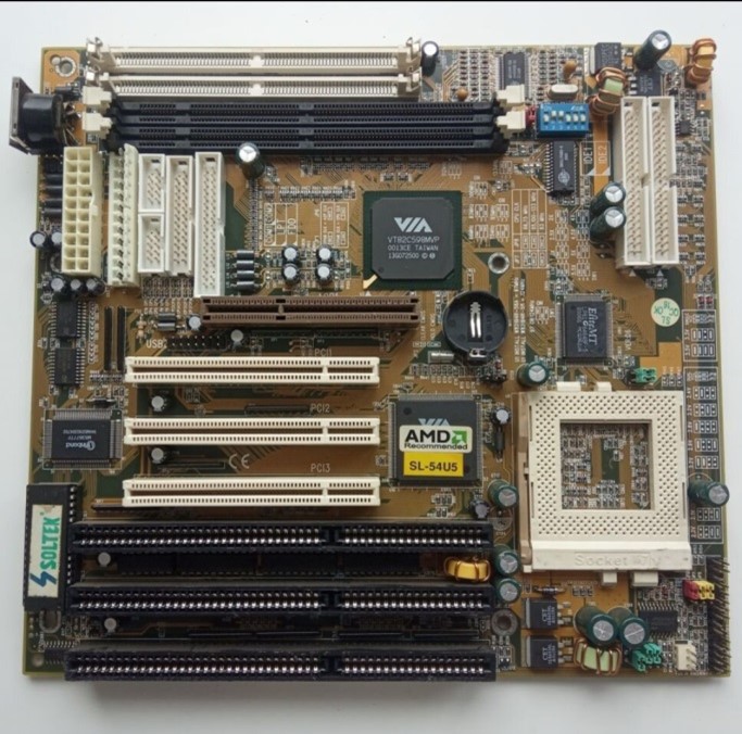
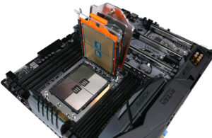
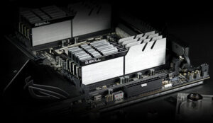
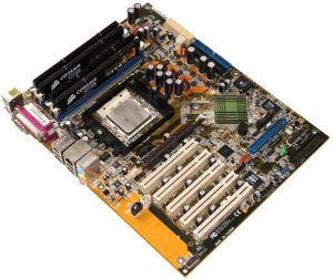
Posted in:
Boards and Systems

September 29th, 2022 ~ by admin

Socialist Romania Computer Chips

The socialist bloc of countries that arose after World War II was not a monolithic entity, it had significant country and cultural differences. A number of countries stood apart, one of them was socialist Romania. The leadership of Romania pursued a relatively free domestic and foreign policy, while remaining within the framework of the socialist system and being a strategic ally of the USSR and a member of the Warsaw Pact.

Rombac 1-11 – National Treasure of Romania

Through the CMEA (Council for Mutual Economic Assistance), the USSR assigned Romania the role of a supplier of agricultural products. The “big brother” proposed to mothball the agrarian backwardness of the republic, which did not suit Bucharest at all. In the late 60s, Romania chose to stand on the path of intensive industrialization. Hydroelectric dams block the Carpathian rivers, and then the Danube. Light industry plants work at their maximum capacity – thus, the country becomes the largest exporter of textiles in Europe. Enterprises of ferrous and non-ferrous metallurgy, chemical and petrochemical, and furniture industries were built. The extraction of precious and non-ferrous metals, uranium, oil, gas, coal were developed intensively. Since the early 1970s, Romanian enterprises have been producing large numbers of machine tools, turbines for power plants, cars, locomotives, tractors, combines, trucks, and household appliances. In the summer of 1979, Romania bought a license from British BAE Systems to produce the BAC 1-11 passenger jet. It was produced at the purpose-built Romaero plant in Bucharest. In total, under Ceausescu, 9 Rombac 1-11 planes were built.

At the beginning of the 1980’s, there were two entities in Romania that produced electronic components, IPRS and ICCE

IPRS-Băneasa, Bucharest. By the early 1980s, the company had over 6,000 employees and nine production facilities. It was located on 15 hectares (37 acres) of land on the edge of the Băneasa forest near Bucharest. Products (capacitors‎, diodes, analog and digital ICs, thyristors, transistors) were sent not only to the countries of the socialist bloc, but also to Asia and Western Europe.


ICCE  (Research Institute of Electronic Components) was built outside the premises of IPRS-Băneasa, but in close proximity. In 1979, the micro-production department of the institute was opened. From that moment on, ICCE was able to supply many of the components developed at the institute, namely those that were requested in relatively small quantities (thousands per month) and which IPRS-Băneasa did not produce because it was not economically viable. Thus, it can be said that ICCE was not a real competitor for IPRS-Băneasa, but rather an addition. For example, in the 1980s, so-called special programs appeared, required electronic components for the Oltcit plant, for the heavy water plant in Turnu Severin, for the nuclear power plant in Cernavodă, as well as for the army. These components were needed in relatively small quantities, with harsh operating conditions carefully selected through reliability programs.

But a third entity that appeared later is of much interest to us, Microelectronica (ME) was set up in 1981 close to I.P.R.S. and ICCE with the goal of manufacturing PMOS, NMOS, and CMOS integrated circuits as well as optoelectronics, complementing the production profile of I.P.R.S. At its inception, ME had about 40-50 employees, most of them engineers, representing the Microelectronics group at ICCE.

Read More »

September 14th, 2022 ~ by admin

The History of the SUPER HEDT x86 PC

Introduction

Last time we talked about the history of the development of high-end computers or High-End Desktop PC (HEDT). In the discussion of the article, some readers remembered motherboards that belonged to HEDT, but were one step higher, both in terms of their technical characteristics and in terms of the cost of ownership of the entire platform based on them. It is possible to name such very high-performance systems – Super HEDT, which often also had their own personal names, and we will talk about them this time.

Last time, the date of the appearance of Intel processors for LGA1366 and the announcement of the first motherboards for them was taken as the beginning of the countdown for the announcement of the HEDT platform. This event happened in the fall of 2008. The reason for the appearance of such platforms was dictated by the decision of the main chipmaker to create two platforms: one for all consumers, and the second specifically for enthusiasts who are ready to get additional performance and new features for extra money that were not available (or needed) for owners of conventional desktop platforms. The logic of making such a decision is simple and logical, but with Super HEDT platforms things are somewhat different.

There may be several reasons for the emergence of such platforms. One of which is to show a competitor that we can do even it better and even faster, to make performance extremes, at the cost of incredible efforts of engineers and, as a result, an incredibly high final price for the end user. Although, for such systems, the price, although it plays an important role, is not a deterrent, because there will always be enthusiasts who are willing to pay as much as the manufacturer dictates to have the very best.

By announcing such a platform, the manufacturer can be sure that the fame and success of his Super HEDT platform will smoothly spill over to his other products, even in the budget segment, because if he is capable of producing a Super “miracle” of engineering, then all of his products, will also have the same properties as the miracle ones, only they will be slower performance and a reasonable price. Super HEDT aura and advertising will do their job and competitors will be forced to return from heaven to earth, because they will have nothing to answer.

The second reason for the appearance of such systems may be for a diametrically opposite reason –  when the manufacturer fails to defeat a competitor on his football field and the only way out is to continue the game somewhere in the orbit of the planet, where the opponent will definitely not fly. Your own personal field – your own rules, even if the price of such a decision will also be cosmically high and beyond the reach of most earthlings. But they will talk about such a decision, though not for long, but long enough to lift you up onto the podium of media fame for a brief time..

And oddly enough, the first Super HEDT system recalled in this article will be the system that was born according to the second, more pessimistic scenario. Has anyone already guessed it?

To find the answer to this question, we will have to go back in time to the very end of November 2006. At this time, the golden years of AMD had already passed, the dominance of its extremely successful Socket 939 and the fastest single-core processors, which included the various Athlon 64 FX’s, had ended. With the introduction of new revolutionary Intel Core processors to the market, AMD had been cornered with its Socket AM2. The market turned towards multi-core, and AMD had nothing to boast of in performance per core. The appearance of the first quad-core Intel Core 2 Quad processors completely deprived AMD of any chance for worthy competition.

If you look at the range of processors available on the market in the fall of 2006, AMD had different Athlon 64 X2’s, manufactured according on a rather outdated 90 nm process technology, the fastest model was the Athlon 64 X2, 5200+ with a real clock speed of 2.6 GHz and a processor for ” green” enthusiasts, the Athlon 64 FX-62 with a clock frequency of 2.8 GHz and a recommended price of $1031. At this time, Intel was selling the Core 2 Duo E6700 with a clock frequency of 2.66 GHz and a recommended price of $530 and a dual-core flagship Core 2 Extreme X6800 at 2.93 GHz, 1066 MHz FSB and 4MB of L2 cache. The cost of all Extreme Editions then was $999. But in November, Intel got its first 4-core processors based on the “Kentsfield” core. The Intel Core 2 Extreme QX6700 was clocked at 2.66 GHz and became the first halo chip, and then more “popular” models followed to conquer the market. The “Kentsfield” core itself was not an honest “quad-core”, it consisted of two Core 2 Duo cores placed on the same substrate. (Hello to all chiplets, and a separate AMD Ryzen) Well, AMD did not go well with its Phenoms, but something had to be done, at least for the sake of media noise.

Core 2 Extreme X6800

The recipe for such an answer is always the same: let’s take our server platform, embellish it a little, adapt the BIOS for enthusiasts, and give the server processor a free multiplier. We will make the number of sockets more than one and the answer is ready. But server systems have a lot of limitations, besides, some of them are hardware-based and cannot be adapted to desktop standards. But in such cases, there is no time for compromises, it is better to sacrifice functionality, performance will not suffer much from this.


AMD Quadfather

Read More »

Posted in:
Boards and Systems

August 24th, 2022 ~ by admin

The Soviet CMOS 8085 CPU: 1821VM85A

Omitting the history of the creation of the first microprocessors (such as the 4004) , let’s turn to the moment when 8-bit microprocessors (Intel 8080 and  8085, Motorola 6800 and Zilog Z80 ) firmly conquered the market. It was the time of the second half of the seventies in the last century. It became obvious to specialists that the future belongs to microprocessors, and if you do not invest in these technologies, you will simply fall out of the number of the developed countries. This was well understood by the advisers to the leaders of the USSR at that time. But they also understood that, since the countries of the Eastern Bloc were somewhat late in this work from US, it would be wise to copy the microprocessors already developed overseas. After all, these microprocessors have already solved many of those problems that would take months and years to solve on their own, not to mention huge monetary costs. (It should be noted that the Soviet Union had its own original developments. For example, the 587 series microprocessor kit, this included three microcircuits.)

587IK1 587IK2 587IK3

At that time, it was not clear which chip needed to be copied – Intel, Motorola or Zilog. Each of them was good in its own way, and it was impossible to predict the outcome of the competition between them. In the end, it was decided to copy all microprocessors. And in order not to scatter forces, the enterprises of the USSR were entrusted with copying Intel products. Little Bulgaria got Motorola and Zilog chips were copied in East Germany. This is how Intel, without investing a single dollar, conquered the Soviet market. Microprocessors and microcontrollers under the names 580IK80A (8080A), 1821VM85A (80C85A), 1816VE48 (8048), 1816VE51 (8051)  became native to Soviet electronic engineers.

1821VM85A

The hero of this article is the 1821VM85A-8 bit microprocessor, a functional analogue of Intel 8085A (but in CMOS). It has been developed since the beginning of the 80s at the Novosibirsk plant of semiconductor devices. Production began in 1985. According to Wikipedia, the manufacturing technology is CMOS, 3 microns. According to other sources 0.7 microns, silicone-on-sapphire. Clock frequency – 5 MHz. Theoretically, it can work at a higher frequency.

The die contains about 6500 transistors. When copying the 80C85, several schematic and topological errors were corrected. As a result, the analogue saves stored data without a minimum clock, but the original does not. This manifests itself when the clock frequency changes. When it is reduced to zero, the microprocessor falls asleep, but the contents of all registers remain unchanged. When clocking resumes, the microprocessor continues to execute the program from where it left off.

It was produced in both ceramic and plastic 40-pin DIP packages.

IM1821VM85A – 1990

IKM1821VM85 (tin pins) – 2012

military grade M1821VM85A – 1993

KM1821VM85 – 1991

IKR1821VM85A – 1994

KR1821VM85A – 1996

At the beginning of the marking of microprocessors, the letters I (И), K, M could be used. I did not succeed in finding out the meaning of the letter I (И) in the marking. Sometimes the letter A is missing from the microprocessor name. The letter I (И) is often present in the marking of the chips of the Novosibirsk plant of semiconductor devices. Here is an example of a microcontroller from this manufacturer.

IKM1850VE39 – 80C39 MCU from 1991

Marking the production date on chips was done in two ways. The first is the usual one, consisting of four digits. The first two digits are the year of manufacture, the second two digits are the week of that year. The second marking method corresponds to this table.

Read More »

Posted in:
CPU of the Day

July 14th, 2022 ~ by admin

The History of the HEDT x86 PC – Part 2 – AMD

AMD’s debut in the HEDT market

Part 2 of the History of the HEDT – See Part 1 (Intro + Intel)

2017

The debut of the AMD High-End Desktop platform happened in the fall of 2017. For his main competitor, he was unexpected and even shrouded in some mystery. In March 2017, the first models of the AMD Zen microarchitecture processors appeared on store shelves, they were the first Ryzen, where the flagship was the 8-core AMD Ryzen 7 1800X, priced at a modest $499. At that time, Intel’s flagship in the desktop segment was the Core i7-7700K, which belongs to the Kaby Lake microarchitecture and had only 4 cores capable of processing 8 threads. The cost of the Core i7-7700K was then $350. The new six-core new flagship Coffee Lake microarchitecture Intel Core i7-8700K would only appear six months later at a price of $370.

AMD planned to release processors with the ZEN microarchitecture for the desktop, mobile and server markets, it did not originally plan to release HEDT processors.

The appearance on the market of AMD Ryzen Threadripper processors has been shrouded in mystery. According to one version, the merit of their appearance lies with the enthusiasm of a small group of AMD engineers who, in their spare time from their main work, experimented with creating a high-performance processor that could be even more productive than the desktop Ryzen. A group of enthusiasts have been working on this project for about a year, and at the end of the work they presented their developments to the company’s management, which, in turn, considered them promising and allocated the necessary funding for commercial development.

Socket TR4

Until May 2017, no one knew about the work on these processors, which would then be called the Ryzen Threadripper. In August 2017, the long-awaited announcement of the first HEDT platform from AMD with three models of AMD Ryzen Threadripper processors happened. The processors were installed in the new TR4 socket with a crazy number of contacts at that time, 4094 contacts. The most basic Ryzen Threadripper 1900X ran at 3.8 GHz, had 16 MB of L3 cache, and had 8 cores capable of processing 16 threads. Such a processor cost $549. The average was the Ryzen Threadripper 1920X with 12 cores and 32MB of L3 cache. Such a processor cost already $799. Twelve-core HEDT competitor from Intel with thermal paste under the cover – Core i9-7920X cost $1199. The flagship of the entire HEDT line from AMD was the 16-core Ryzen Threadripper 1950X, which was estimated at $999. Intel’s 16-core counterpart, the Core i9-7960X, was offered to enthusiasts at a price one and a half times more expensive, for $1,699.

What did AMD’s first HEDT platform offer to wealthy enthusiasts?

Read More »

Posted in:
Boards and Systems

July 11th, 2022 ~ by admin

The History of the HEDT x86 PC – Part 1

Introduction

In this article, I would like to recall how the history of high-end computers or High-End Desktop PC (HEDT) began, what we now have in this segment, and what awaits us in the near future.

Until a certain point in time, the computer market for personal computers was not divided into subcategories. There was the concept of a personal computer, where its main criteria were: performance and cost. The higher the performance, the more expensive such a PC was. There was and still are ‘Workstation’ class PC’s but these are really more of a Business class (think CAD or Video editing) then what you would buy for your house. The problem of insufficient performance was solved for a very long time with the help of overclocking and it would seem that this order of things suited everyone.

If you want a faster video card or processor, buy the Top model. Until a certain point in time, everything was like that, but at the beginning of the 2000s, processor manufacturers realized that there was a certain group of buyers who were willing to pay more. Then they were called “enthusiasts”, and now they have been renamed “gamers”. Since 2003, Intel, in unison with AMD, has been releasing their processors for wealthy enthusiasts. The first processor model from “blue” was the – Pentium 4 Extreme Edition with a clock frequency of 3.2 GHz and a very nice price of $999 (A Celeron of that era was around $100 for 2.5-2.8GHz).

Thus, in this processor model, a beautiful and memorable cost, a defiant name and technological sophistication, the roots of which go deep into the server segment, are combined. The owners of the “extreme desktop processor” already considered themselves a completely different caste, and no overclocking of the older processor model could give an ordinary user the performance that an enthusiast had, and after all, extreme processors were also overclocked.

At first, AMD generally went the other way, a special separate platform was created for enthusiasts, where processors with their own separate socket were installed. Thus, the segmentation of the personal PC class took place at the physical level. We are talking about AMD Athlon 64 FX processors, and to be more precise, about the first model of this family – AMD Athlon 64 FX-51. I would call them timeless classics, still using a ceramic package, a separate socket, and special registered DDR-SRAM memory.

The release of these desktop processors for enthusiasts also marked the beginning of a new 64-bit era and changed the leaders of the processor industry. The yellow jersey of the leader shone on a green “background”, and Intel moved into the camp of catching up. As revenues and the image component of users and enthusiasts grew, marketers and simple engineers did not sit idly by. Performance is never enough (although it seems to me that for the last 5 years it has definitely been enough in any products of the middle-end segment) and something had to be offered to enthusiasts who were willing to pay even more. I suppose that such wealthy enthusiasts are now called creators or a close meaning of this term.

HEDT from Intel

Read More »

Posted in:
Boards and Systems

June 30th, 2022 ~ by admin

Chip of the Day: Soviet 573RF10 – a CMOS 8755A

Intel released the i8755 in 1976, the i8755A in 1977 (with better compatibility with the 8085A and 8086/8). The Intel 8755 is an UV- erasable and electrically reprogrammable ROM (UV-EPROM) and I/O chip. The EPROM portion has 16 384 bits, organized as 2048 words by 8 bits. The I/O portion has two general purpose I/O ports, each I/O port is individually programmable as input or output.  These were essentially a combination of the 8255 PIO and the 2716 EPROM on a single die/package. These were made on a NMOS process.

Intel C8755-8 – 1977

Intel C8755A – 1979

NEC D8755AD -1981

Toshiba TMP8755AC ’83

NEC and Toshiba released similar microcircuits behind Intel. Basically, the microcircuit was intended to work together with the 8085A microprocessor. It differs from its predecessor i8080A in that it has a multiplexed data and lower address bus. The standard three-bus architecture of the microprocessor system is obtained by multiplexing with the help of an additional external register. In this register, the low byte of the address is fixed by the special output signal of the microprocessor.

Intel 87C75PF Engineering Sample – 1988

By 1988, the 8755A was obsolete and Intel released the 87C75 instead (see article on the CMOS 87C75).

Novosibirsk IM1821VM85A – 1989

Around this time, the production of an analogue of the i8755A, the 573RF10 microcircuit, began in the Soviet Union. Why start producing a microchip that the world electronics leader is changing to a more advanced one? The fact is that at the beginning of 1988, the production of IM1821VM85A began in the USSR. This was a radiation hard analogue of the CMOS i80C85A. It was with it that the 573RF10 was supposed to work.

K573RF10E (gold pins) 1990

KM573RF10 – Gold ’92 / tin pins ’93

The chip is made in a 40-pin side-brazed ceramic DIP. Supply voltage +5 V. Programming voltage +21 V. It was produced at the Vostok fab in Novosibirsk on a CMOS process (to match the 80C85A).

Unmarked 573RF10

The 573RF10 is the only CMOS chip in the 573 series.

573RF10 die – single memory cell – radiopicture.listbb.ru

Intel 8755A die – 2 memory cells – cpu-galaxy.at

It is noticeable to the naked eye that the 573RF10 is own Soviet development. The 573RF10 and i8755A dies are completely different. The i8755 has two memory arrays clearly visible, while the 573RF10 has only one.
It must be said that the application of the 573RF10 chip was not wide enough. And in general, the idea did not take root. The next obvious step in evolution was the combination of a microprocessor, ROM and RAM, input-output ports in one chip which was frequently done on the MCS-48 and MCS-51 series MCU’s which were also being produced in the Soviet Union at the time.

Written by guest author Vladimir Yakovlev
Edited/Formatted by John Culver – The CPU Shack Museum
Pictures – The CPU Shack Museum and others

Posted in:
CPU of the Day

June 13th, 2022 ~ by admin

The History of Angstrem Memory IC’s in the USSR

This article is about memory chips manufactured by one of the entities – the leader of the electronic industry of the USSR – Angstrem. As you know, the Soviet Union ceased to exist in December 1991. We restrict ourselves to the development period of the considered memory chips produced at Angstrem, the end of 1991. Let’s make an attempt to track how the capacity of memory chips grew, how technologies were improved that allowed the Soviet Union not to let the world leaders in electronics go far from itself at that time. A small example: Angstrem’s Dynamic RAM 4K went into mass production in mid-1975, Intel introduced its own in 1974. Intel launched a 16K DRAM in 1977, and Angstrem released its counterpart in 1978.

Angstrem Headquarters

Angstrem was established in June 1963 in Zelenograd (outside of Moscow) as a pilot plant in conjunction with the Scientific Research Institute of Precision Technology. At Angstrem, new technologies for the production of microelectronics were developed, and pilot batches of new microcircuits were also produced. The debugged production technology was then transferred to other enterprises of the USSR and countries of Eastern Europe.
The development and manufacture of memory chips was one of the main activities of Angstrem. It was on them that new semiconductor structures and production technologies were more effectively worked out, and the stability of obtaining finished products is considered in world electronics as a sign of technology ownership. It’s relatively easy to make a small batch of good chips, it’s hard to make a process whereby a large amount of chips can be made and be reliable. It was the very low chip yield percentage that played a cruel joke on Angstrem when mastering the production process of the DRAM 565RU7 chip.

SRAM

In 1966, Angstrem created the first MOSFET in the USSR, which was the first step towards the strict goal of creating CMOS integrated circuits. The first CMOS microcircuit, created in the Soviet Union in 1971, was the 16-bit Angstrom matrix of memory cells 1YaM881.The supply voltage is 6 volts instead of 5 volts, like the rest of the chips in this series.

1YaM881 – 1972

The next in a series of static RAM chips was the CMOS K561RU2 (K564RU2), released in 1976. 564 series of chips is a “military” analogue of the 561 series. In these series, there are several dozen microcircuits. The chip has an organization of 256 words by 1 bit.

561RU2 die – 16×16 256bit matrix clearly visible – The image is taken from the site https://radiopicture.listbb.ru/ with the permission of the author.

It contains 2067 integral elements. Supply voltage is 3-15 volts. It’s an analogue of CD4061A.  It should be noted that in most cases ‘analogue’ means similar to, not an exact copy or exactly compatible.  The USSR did make some compatible IC’s, but they mostly made stuff that was similar, but built to their own specifications/needs.


K564RU2A -1978

K561RU2 -1979

The package of the K561RU2 chip is wider than the standard packages of this series.

K565RU2 -1979

The K565RU2 static RAM chip was manufactured using NMOS technology. Chip capacity was 1024 bits (1024×1). Contains 7142 integral elements. An analogue of Intel 2102A, developed in 1974. K565RU2 appeared in 1977. It was originally designed to be placed in a ceramic package, but later, in order to reduce the cost of production, the dies began to be packed in plastic packages.

Read More »

Posted in:
CPU of the Day

June 5th, 2022 ~ by admin

CPU of the Day: P.A. Semi PA6T PowerPC

When Apple bought P.A. Semi back in 2008 it was the beginning of the era of the iPhone, and their was much speculation as to why Apple was buying a company that made low power high performance PowerPC processors.  Especially since the iPhone ran on ARM and the Mac had moved from PowerPC to x86.

P.A. Semi PA6T-1682M

P.A. Semi was started in 2003 by Daniel Dobberpuhl (who passed away in 2019).  Dobberpuhl was one of the truly greats of microprocessor design, with a career starting at DEC on the T-11 and MicroVAX, before helping DEC transition to the Alpha RISC design (21064).  It was Dobberpuhl who started the design center in Pal Alto (where P.A. Semi would later take its name from) that designed the DEC StrongARM processor.  A processor that was later purchased by Intel and became the XScale line of ARM processors.

After Intel bought the StrongARM line, he then helped start SiByte, making MIPS based RISC CPUs, and continued to do so when SiByte was purchased by Broadcom. So when he started P.A. Semi it was less about PowerPC and more about RISC, PowerPC just happened to be the architecture they chose to use.  The design team had extensive experience on a variety of CPU architectures, including SPARC, Itanium, and the early Opterons.  You can see why this acquisition was so attractive to Apple.

PA6T block diagram

In the few years (2003-2008) from when P.A. was founded to when Apple took them over, they did design, market, and sell a PowerPC processor line called PWRficient based on what they called the PA6T core.  The PA6T-1682M was a Dual core PowerPC processor (the 13xxM was the single core version) with each core running at up to 2GHz with 64K of L1 Instruction cache and 64K of L1 Data cache.  They were fab’d on a 65nm process by TI and ran at 1.1V.  The L2 cache was scalable and shared amongst the cores.  In the 1682M this was a 2M 8-way cache with ECC.  One of the most useful features was their clock stepping.  They could drop to 500MHz at only a few watts per core, and then back up to the full 2GHz in 25us.

AmigaOne X1000 (made by Aeon) PA6T-1682M

The PA6T was only on the marked for a few months (from the end of 2007 to April 2008) before Apple bought them for $300 million, but in this time P.A. Semi had numerous design wins.  Amiga selected it for use in the AmigaOne X1000 computer.  The AmigaOne did not hit market until 2011, which means that while P.A. Semi was bought and completely under control of Apple, they still continued to make, support, and supply their previous customers with the 1682M CPU.  Certainly Amiga wouldn’t be big enough to push Apple to continue making a chip?

They were not, but others were, and the PA6T was such a great processor that it had been selected and designed in to many computer system used by US Defense contractors, and if anyone doesn’t like change, its Defense contractors, so with some prodding by the US Dept of Defense Apple continued to make (or rather have TI make) the PA6T processors.  Curtis-Wright had designed the PA6T into their new CHAMP-AV5 DSP VME64 board, which was used for signals processing across numerous military applications.  They also also used the PA6T (at 1.5GHz) in the VPX3-125 SBC. Themis computers, NEC, Mercury and others designed in the PA6T. Extreme Engineering, another maker of PA6T based boards, referred to the design as ‘ground breaking.’

Extreme Engineering XPedite8070 SBC

It would have been interesting to see what P.A. Semi could have achieved had they not been gobbled up by Apple.  Clearly we see the results of the talent of the P.A. team in what Apple was able to accomplish with their A-series processors, but clearly P.A. had something special for the PowerPC architecture as well.

Tags:
, ,

Posted in:
CPU of the Day