The DEC/Compaq Turbo Laser 6 AlphaServer KN7CH Processor
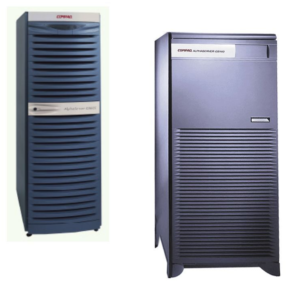
AlphaServer GS60 and GS140
The DEC TurboLaser 8200/8400 was a series of high end Windows NT compatible servers/workstations introduced in 1995. After DEC was sold to Compaq (in 1998) the 8200/8400 were upgraded from the EV5/EV56 (21164/21164A) to the 21264/21264A (EV6/EV67). Compaq wasn’t as bold with code names it seems so instead of being referred to as the TurboLaser they were simply called the TL6. The machines themselves were also renamed from the 8200 to the GS60 and the higher end 8400 to the GS140. GS referring to ‘Global Solution’ to reflect Compaq’s international marketing of the computers. The GS60 was the lower end rackmount model supporting up to 6 CPUs and 12GB of RAM and the GS140 full cabinet model supporting up to 14 CPU and 28GB of RAM. Both could be configured with either 21264 525MHz CPUs with 4MB of B-cache each or 700MHz 21264A CPUs with 8MB of B-cache each. The 21264A added support for writeback cache, as well as its faster speeds and some new instruction set extensions. Initially availability of these systems was in late November of 1999, coinciding with the release of the 21264A CPUs. By the time of their release Alpha support for Windows NT was lagging, so most if not all systems were sold with Tru64 UNIX or OpenVMS OS.
The GS60/140 were large cases similar to a rackmount system but self contained. The processor modules for them contained a pair of CPUs, the cache for the CPUs and the entire chipset. They connected to the main computer with a very large connector that provided power (48VDC) as well as all the Memory/IO and clock signaling. This was referred to as the TLSB (TurboLaser System Bus). The fastest of these was the KN7CH (also known as the E2067-DA) which had dual 700MHz 21264A processors with 8MB of Cache each.
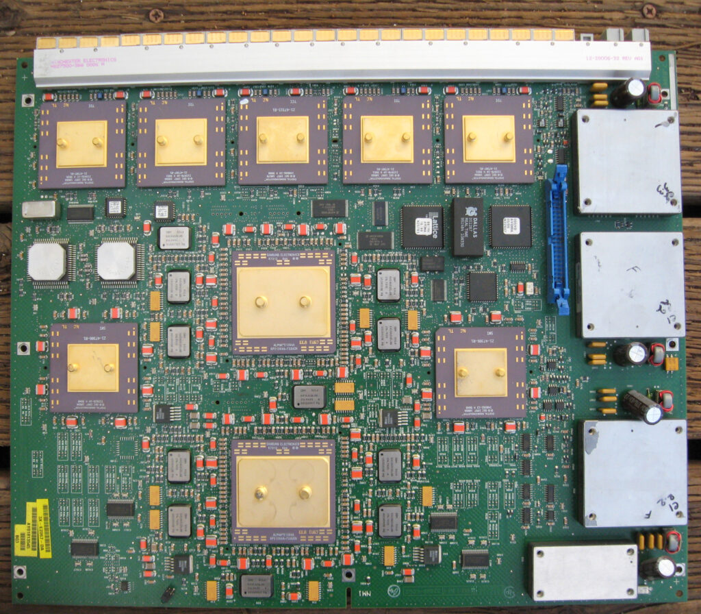
DEC KN7CH 6/700 Processor Board
This processor board is quite interesting, its a rather early board (PLDs are dated March of 2000) and the pair of Samsung 21264A processors are dated 9944, these are some of the very first production 21264As. Also of interest is that these Samsung CPUs are 733MHz models (KP21264A-733UCN). The 21264A was to be made in 600, 650, 667, 700, 733, and 750MHz versions, though I have only actually seen 667 and 733MHz versions. Making only 2 speed grades of the processor would greatly simplify testing and logistics, and with a rather limited customer base, there wasn’t a clear marketing need to make so many different speeds, these were not CPUs that were generally available outside of OEM use. These servers were also designed to be high reliability systems, running a 733MHz rated CPU at 700MHz would increase reliability by decreasing heat related wear and tear.
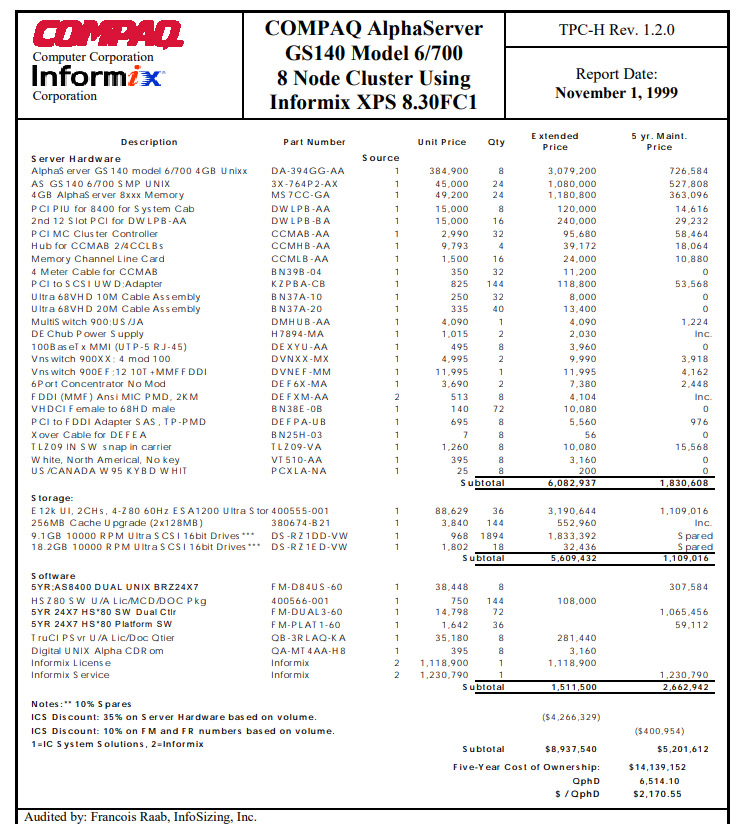
Build Sheet for a 8-Node GS140 with Eight 6 CPU GS140 6/700 Systems. Each with 12GB of RAM. A nice $9 million system
The entry price for the AlphaServer GS60 with 4 GB of memory was $199,990 ($340,000 in 2022). The AlphaServer GS140 system price started at $399,400 ($680,000 in 2022). These were very expensive systems. One look at the processor board shows what that kind of expense gets you, a whole lot of gold. Its hard to find another computer system built in 2000 that has 9 gold/ceramic chips on each processor board. A single dual processor board was $45,000 ($76,000 in 2022USD), and each 4GB of RAM was another $49,000. One can easily see how such a system could quickly cost several million dollars. Each of these boards cost as much as a really nice car! Lets look at what that $45,000 gets you
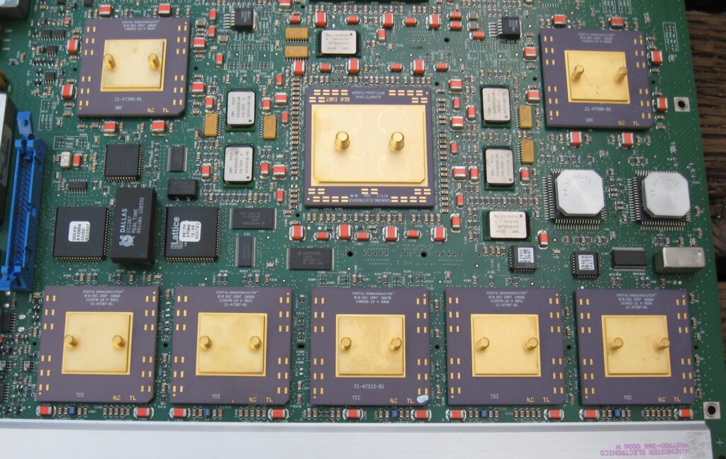
Top Row (L->R) SWI, Alpha 21264A, SWI – Bottom Row: TDI, TDI, TCC, TDI, TDI
2x KP21264A-733UCN. Each 21264A chip has a separate address and data bus for the B-cache and system operations. The 21264A chip has a 64-Kbyte instruction cache and a 64-Kbyte data cache. These are made by Samsung on a 0.25u process and dissipate 85Watts at 2.0V.
20x IBM SRAM Cache Memory: 8-Mbyte ECC L2 cache per CPU made using 16x IBM 0418A81QLAA-4 512Kx18 8Mb ECC SRAM chips and 2x 128Kx36 / 2x 256×18 for the TAG RAM
2x DEC 21-47306-01 SWI: Two swizzle (SWI) chips receive data from the 256-bit wide DLSB (the DEC Local Bus) and pass it to one of the CPU chips over the 64-bit wide data interface bus. These are located on either side of the pair of CPUs.
4x DEC 21-47307-01 TDI: Four TurboLaser Data Interface (TDI) chips receive data from the TLSB (the main system bus that connects all cards in the system) and pass the data over the DLSB to the two SWI chips. These are the outer 4 chips on each end of the row of 5 gold chips on the bottom. Each one handles 64-bits of the 256-bit TLSB.
1x DEC 21-47315-01 TCC: The TurboLaser control chip (TCC) takes commands from both CPUs and issues them to the TLSB. It also controls all data movements through the TDI and SWI chips. This is the center chip between the pairs of TDI chips.
2x AMD AM29F080DB-90EC: 5V 8Mbit Flash for the system firmware
4x Galaxy Power DC-DC Converters. These regulate down the 48VDC supplied by the systems redundant power supplies to the voltages needed for the board. There is a pair of 2.2V 7A converters for the CPUs, and a 7A 3.3V converter for all the I/O. There also is a smaller 2A converter of unknown voltage (likely 5V).
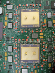
Pair of Samsung KP21264A-733 Processors surrounded by cache chips
The TurboLaser line was replaced in 2002 by the WildFire servers (GS80, GS160 and GS320) which upgraded the CPU support to 32 21264Cs with 256GB of RAM. Unfortunately by this time Compaq had merged with HP and the combined server line was a bit cluttered, having Alpha, PA-RISC, Itanium and Xeon based systems. The Wildfire and its Marvel follow on were the end of the road for the Alpha. Unfortunately the same thing happened with the PA-RISC and Itanium (ok maybe not so unfortunately with Itanic) as well. The days of boards full of golden RISC are past, replaced by BGAs with enormous heatsinks.


March 27th, 2022 at 2:55 am
Where are the cache chips? Are they packaged on the CPU as an MCM?
March 27th, 2022 at 8:36 am
The B-Cache (L2 Cache) are the silver covered (IBM) chips around each of the CPUs (there are some on the back of the board too)