Archive for the 'CPU of the Day' Category

October 6th, 2013 ~ by admin

Decryption by an Intel 80386 – Military Style

Raytheon KGV-25

Raytheon KGV-25 – Click to Enlarge

Sometimes we get processors in on boards that are just too interesting, or too good looking to remove.  That is the case with this KGV-25 correlator board.  It is a processing systems used for decrypting communications that was in wide use by the US (and likely other) militaries in the 1990’s.  The KGV-25 could receive encrypted UHF data at rates of up to 400Mbps as part of the Multi-Mission Advanced Tactical Terminal (MATT). More information on the MATT can be found here on the FAS website.

As is typical of military equipment the system did not use the latest and greatest available at the time (this board is from 1994 so the Pentium era).  The board is run by a time proven and reliable Intel 80386 processor running at 25MHz. In addition to the MQ80386-25/B (MIL-STD-883B spec 386 processor) the board contains:
Intel MQ82380-20/B  – DMA Controller for interfacing with all the assorted SRAM on the board
Intel MQ82592/B – LAN Controller for interfacing with the rest of the system
VLSI VM05403 USART – Universal Asynch/Synch Receiver Transmitter
and on the back is a MQ80387-25/B Math-coprocessor for the 386 and 4MB of 35ns SRAM

Raytheon KGV-25 - Back

Essentially a complete 80386 system, of similar performance to a higher end system int he late 1980’s.  Just with a lot more gold, and built to take a lot more abuse then your average beige box of the 80’s


Posted in:
CPU of the Day

September 28th, 2013 ~ by admin

Realtek RTL8186: MIPS by Lexra

Realtek RTL8186 Lexra LX5280 MIPS with DSP Extentions - 2006

Realtek RTL8186 Lexra LX5280 MIPS with DSP Extensions – 2006

The MIPS architecture was created in 1985 from a project at Stanford University.  It was one of the first licenseable architectures.  A company could buy a license and make their own MIPS architecture processors.  By the 1990’s this had become fairly common and many companies were making MIPS processors, including Performance Semiconductor, IDT, NEC, Toshiba, LSI and more.  In 1992 MIPS Computer Systems, Inc. was bought by SGI, in order to guarantee a supply a continued development of new MIPS designs for SGIs computers.  It did continue to license the design to other companies as well, fostering competition which helped lower prices for SGI.  In 1998 SGI spun off MIPS into its own company once again, as SGI at the time had decided to move towards Intel’s Itanium architecture (this should sound familiar, DEC and the Alpha suffered the same fate).  By 2008 MIPS was losing money and in 2013 what little remained (having used most of their cash to buy, and then sell at a loss Chipidea) of them was bought by Imagination Technologies (makers of the PowerVR line of graphic solutions, used notably in the Apple iPhone’s A4, A5, A6, and likely A7 processors).  But there is a bit more to the story of MIPS, a seemingly small chapter that very well could have changed history and certainly changed the success of MIPS.

In 1997 a small company called Lexra was started. Lexra was a semiconductor Intellectual Property company.  They designed processors and licensed the designs.  What made Lexra different is that they designed and licensed soft-cores.  A soft core is an RTL (Register Transfer Level) model of the processor.  It is usually written and delivered in an HDL (Hardware Descriptive Language) such as Verilog or VHDL and the purchaser may compile it down to whatever actual transistor level hardware they like.  This is exactly how ARM works today, but in 1997 ARM only licensed hard cores, cores already compiled down to the gate level and ready for implementation on a given fab process technology.  This allowed them to have tighter control over the design and its performance, but made integration much harder into other products.  A soft core like Lexra designed enabled rapid integration into a variety of SoCs and other applications.  Lexra’s chosen architecture was MIPS and that is where the story gets interesting.

Read More »

Tags:
, ,

Posted in:
CPU of the Day

September 15th, 2013 ~ by admin

Compaq 21364 Processor – The Omega of the Alpha

Compaq 21364 Alpha Prototype - 2002

Compaq 21364 Alpha Prototype – 2002

The DEC Alpha was one of the fastest processors of the 1990’s. The original 21064, manufactured in CMOS, rivaled the fastest ECL processors and blew away most everything else.  Clock speeds were 150-200MHz (eventually hitting 275MHz) at a time when a standard Intel PC was hitting 66MHz, at the very top end. It was manufactured on a 0.75u process using 1.68 million transistors.  The Alpha was a 64-bit RISC design, at a time when 16-bit computing was still rather common.  This gave the architecture a good chance at success and a long life.

The 21064 was followed by the 21164 in 1995 with speeds up to 333MHz on a 0.5u process, now using 9.3million transistors.  It added an on die secondary cache (called the Scache) of 96KB as well as 8KB instruction and Data caches.  These accounted for 7.2 million transistors; the processor core itself was only around 2.1 million, a small increase over the 21064.  At the time the main competition was the Pentium Pro, the HP PA8800 and the MIPS R10000.  Improved versions were made by both DEC and Samsung, increasing clock speeds to 666MHz by 1998.

In 1996 DEC released the next in the series, the 21264.  The 21264 dropped the secondary cache from the die, and implemented it off chip (now called a Bcache).  The level 1 caches were increased to 64KB each for instruction and data resulting in a transistor count rise to 15.2 million, 9.2 million of which were for the cache, and the branch prediction tables.  Frequency eventually reached 1.33GHz on models fab’d by IBM. However the end of the Alpha had already begun. DEC was purchased by Compaq in 1998, in the midst of the development of the enhanced 21264A.  Compaq was an Intel customer, and Intel was developing something special to compete with the Alpha.

Read More »

Tags:
, , , ,

Posted in:
CPU of the Day

September 3rd, 2013 ~ by admin

ARCA: The Processor that came from the East

Arca-1 Rev2 166Mhz - Late 2001

Arca-1 Rev2 166Mhz Processor – Late 2001

China is generally seen as where devices are made or assembled, rather then where they are designed or invented, certainly in the computer world.  In 2001 a Chinese Gov’t funded venture known as ARCA Technologies changed that.  ARCA (Advanced RISC Computer Architecture) designed and released a completely new processor known as the Arca-1.  At the time there were two design houses working to create China’s first CPU. Arca, and BLX.  BLX made the Godson series of processors which are MIPS32 and MIPS64 implementations.  Arca, took a different approach.  Not only did they seek to make an indigenous design, but they wanted to do so with their own Instruction Set Architecture (ISA).

The ArcaISA is, of course, RISC based, it contains 80 instructions, with each instruction consisting of up to 3 operands, and contains 32 general purpose registers.  The original Arca-1 design is made on a 0.25 micron process (by which foundry is unclear, BLX used ST) with a 5-stage pipeline and drawing 1.2W at a clock speed of 166MHz.  It contained separate 32 way associative 8K caches for Instruction and Data.  The Arca also includes a DSP unit that has a pair of multiply/Accumulate Units (MACs) as well as basic SIMD support for media acceleration (including hardware MPEG2).   Not exactly impressive for 2001, but not bad for a first release.  However there was more to come.

Read More »

Tags:
, ,

Posted in:
CPU of the Day

August 31st, 2013 ~ by admin

AMD Am29116: A Bit Better than a Bit Slice Processor

AMD AM29116DC - 1987 10MHz

AMD AM29116DC – 1987 10MHz

In 1980 there was not yet a clear winning architecture for microprocessors.  Many of the companies of the 1970’s were still churning out designs, hoping for design wins.  Intel had yet to become a dominating force, though their 8086 line was becoming popular.  AMD was one of the innovators of the time. Now known for their x86 processor, AMD made many other designs that were very successful.

In 1980 AMD was already making 2 16-bit class processors.  They were a second source for the Intel 8086 (8/16 bit) as well as the primary second source for the Zilog Z8000 processor.  They soon would pick up manufacturing demand for the Intel MCS-51 line as well.  This was not enough for AMD, they sought to design a 16-bit microprocessor that would excel at high speed control applications (such as telecom and disk controllers).  Thus began one of the most ambitious and complex designs of the time.  In order to meet their performance goals the design had to be done in ECL, on a bipolar process, this is a bit more complicated for a large device then a NMOS part, mainly due to its power requirements and heat.

AMD AM29117GC - 1985 - Dual port version

AMD AM29117GC – 1985 – Dual port version

In 1981 AMD announced the Am29116 microprogrammed 16-bit processor.  It was made on a 2 micron process and contained 2500 effective gates (~14,000 transistors, 50mm2 die area).  Max speed was 10 MHz. Samples were available starting in early 1982.  The target competition was not the 8086 or Z8000 but The DEC T-11 ‘Tiny’ processor, which was made in NMOS and ran at 2.5MHz.  The Am29116 is technically a bit-slice processor, like AMD’s wildly successful 2901 processor but adds a bit more functionality including instruction for bit manipulation, CRC generation, as well as a barrel shifter and an on chip scratch pad RAM (32x16bit).  It has an accumulator, ALU, status register, and instruction latching/decoding for the 167 instructions.  What the 29116 lacks is a PC (Program Counter).  Program sequencing is handed by external logic, either custom, or using AMD 29112 microprogram sequencers.  It is the job of the sequencer to feed instructions to the 291116, handled jumps, calls, returns, and memory accesses.  This puts the 29116 somewhere between the basic 2901 and a full featured processor like the Z8000.  AMD also produced the 29117 which added a second 16-bit port, resulting in a dedicated input port (D) and a dedicated output port (Y), whereas the 29116 had a single I/O port.  This allowed for faster processing where data could be read and written simultaneously.  The 29117 was available in a PGA68 package (16 more pins then the DIP52 of the 29116)

Read More »

Posted in:
CPU of the Day

August 3rd, 2013 ~ by admin

MOS Technology MCS6501 Processor

MOS MCS6501 - November 1975

MOS MCS6501 – November 1975

One of the classic stories of the 1970’s microprocessor boom times was that of MOS Technologies at WESCON (Western Electronics Show and Convention) on September 16th 1975 in San Francisco.  MOS Technology was a newcomer to microprocessors.  They had with them two brand new processor design, the MCS6501 and the MCS6502 which they hoped to sell on the floor at Wescon, for $20 and $25 each.  However Wescon forbid sales on the convention floor, so quick thinking by MOS Technologies Chuck Peddle directed people to a hotel room, where “the beer was free and chips were $25.”  In the room were jars of 6501 and 6502 processors, to give them impression that these were in full production.  In reality the bottoms of the jars were filled with defective parts.  It was no matter, the 6500 series was a huge hit, led largely by its availability, low price and marketing to everyone (not just ‘big corporate users’).  The 6500, and specifically the 6501 have an interesting story leading up to that fateful day at WESCON.

Motorola XC6800B - July 1975 - Pre-production part, not something MOS bothered with.

Motorola XC6800B – July 1975 – Pre-production part, not something MOS bothered with.

It begins at Motorola, where Chuck Peddle, Bill Mensch and several others were employed in the early 1970’s design the MC6800 processor and its peripherals.  The 6800 was not a bad design, it was however, very expensive, a development board for it costing over $300.  Chuck worked largely as the 6800 system architect, ensuring all the ICs worked well together and were what was needed to meet customers needs.  He attended many calls to potential clients and noted that many were turned off by one thing, price.  With that in mind he sought out to build a lower cost version of the 6800 using some of the newer processes available (specifically depletion mode NMOS vs the enhancement mode of the 6800).  Motorola management wouldn’t hear it, they wanted nothing to do with a lower cost processor available to the masses.  And with that, Chuck, Bill and over half the 6800 team left.

Read More »

Posted in:
CPU of the Day

July 26th, 2013 ~ by admin

Apple G3 Prototype: The Goleta and IBM Arthur Processor

IBM Arthur Processor - 1997

IBM Arthur Processor – 1997

By 1997 the PowerPC 604e was getting a bit dated.  Apple needed an updated faster processor for their new computers and IBM and Motorola needed a new processor to sell to Apple.  The PowerPC 750 was an evolution of the 604e and became the core of Apple’s various G3 systems.

In early 1997 Apple , IBM, and Motorola (together known as the AIM Alliance) were working on what would become the PowerPC 750.  It’s code name? The Arthur.  Apparently someone at IBM or Motorola had a liking for Sherlock Holmes as the 745 was codenamed Conan and the 755 Doyle, after Sir Arthur Conan Doyle, writer of Sherlock Holmes.  This particular part is date coded R20003PAP which means it was made in mid-May of 1997, 6 months before the G3 and PowerPC 750 were officially released.

The card the Arthur processor (hand labeled 300Mhz) resides on is an Apple Prototype known as the Goleta.  The Goleta was one of the first Apple G3 products.   It was to be used in the PowerMac 9700 aka the PowerExpress which was to be a 6 slot G3 PowerMac running at 275MHz.

Apple Goleta G3 Prototype

Apple Goleta G3 Prototype – Click here to see the full card.

It never made it past the prototype stage.  The card is labeled as serial #014 making it a very early prototype, though how many total were made is not known.  The card may have been used at Apple for testing other deigns as well and certainly was a test bench for the new 750 PowerPC Processor.  This was a chaotic time for Apple as they were struggling to pull out of near bankruptcy.  Steve Jobs had only just returned to the company and radically changed what Apple was doing, and what they were not doing (making money).

Posted in:
CPU of the Day

July 21st, 2013 ~ by admin

CPU of the Day: Intel Pentium Mechanical Sample

Intel Pentium Mechanical Sample - 1994

Intel Pentium Mechanical Sample – 1994

Intel and other processor companies spend a vast amount of time testing a processor design before it is released.  They want to be sure that it meets the specifications set forth in the datasheets and is free of undocumented errata.  Intel gained fame, or notoriety for the FDIV bug int he original Pentiums that caused a certain set of floating point calculations to result in an incorrect answer.  This led to the recall and replacement of many millions of processors.

Operational testing however is only one part of the testing a processor undergoes.  The package itself must also be tested.  It is tested for proper fit and function in a socket and with a variety of cooling apparatuses.  Its thermal characteristics must also be tested.  The original Pentiums were a ceramic package but quickly moved to a package with a heatspreader as they ran very hot.  In additional sample are made for testing the electrical supply of the mainboard, so that mainboard manufacturers may test their VRM (Voltage Regulation Module) design to ensure it can meet the demands of the processor.

A Mechanical Sample, like the early Socket 5 Pentium above, were used to test heatsinks, sockets, and other tasks that did not require a functioning chip.  Usually these samples did include a die (as does this one) they just are pulled from the line before final testing and speed binning.  Mechanical Samples were also used by Intel in their ‘The Journey Inside: The Computer’  education kits which typically included a processor sample, a wafer and some cut processor dies as well as some basic electronics for students to conduct experiments with.  Sometimes Mechanical Samples are devoid of marking, or like this one clearly state what they were intended for.  Some processor companies also made Marketing Samples, which were non-functioning, but often marked with color logos/graphics to advertise the processor.  Both are ivery rare to find as they were made in very limited quantities and were not widely distributed.

June 16th, 2013 ~ by admin

CPU of the Day: Bell Labs BELLMAC-8 aka the WE212

Western Electric WE212B - BELLMAC-8 Processor

Western Electric WE212B – BELLMAC-8 Processor – 1979

Many great technologies have came out of Bell Labs including the C programming language and UNIX.  Bell Labs was the R&D arm of AT&T and developed most everything in house for AT&T.  Bell was loathe to use any product that was not their own, so when the computing age of the 70s came, it was only natural for them to develop an in-house microprocessor to run their telecom systems.

The first processor Bell developed was the BELLMAC-8 in 1977.  The BELLMAC-8 was a fairly simple 8-bit processor containing over 7000 transistors and made on a 5 micron CMOS process.  It ran at up to 2 MHz at 5V (5V and -5V supplies).  It implemented 40 instructions most taking around 4 cycles to complete.  the MAC-8 used a 8-bit data bus and a 16-bit address bus (capable of addressing up to 64 Kbytes of RAM). The BELLMAC-8 is a register based design

BELLMAC-8 Die

BELLMAC-8 Die

with 16 general purpose 16-bit registers.  These registers are stored off chip in memory and an on chip Register pointer register (rp) contains the address of their beginning location in memory.  One could perform register ‘saves’ for IRQ handling by simply changing the value in the register pointer register (and storing the old value on the stack).

There is not a great amount of information on the BELLMAC-8 as it was intended for use within Bell/AT&T.  It was not designed or intended to be a commercial processor.  It was used (and branded) be Western Electric (which was the production arm of AT&T) in many telecom products.  Despite its wide use, very little documentation exists, at least outside of AT&T.  It is not a processor covered in any of the standard books/catalogs (such as IC Master, Osborne or other period microprocessor selection guides), most likely because it was for Bells use exclusively.  There was a trainer system made for the BELLMAC-8 used to teach engineers how to use the processor.  Most produced BELLMAC-8s are labeled as WE212 (or F-60789 on the trainers) and are found in Western Electric products.  The WE212 came in several 40-pin packages, including a version with a gold lid, and a version with a black ceramic lid.   Western Electric made several versions (though no documentation on the differences).  These included both the WE212C and the WE212B.

Western Electric WE32100 - BELMAC-32 Processor

Western Electric WE32100 – BELMAC-32 Processor

In 1979 Bell released the BELLMAC-4, a microcomputer version of the BELLMAC-8 containing on chip ROM and RAM.  It was made on a 3.5 micron process.  In 1980 Bell announced the BELLMAC-80.  The BELLMAC-80 was made on a 2.5 micron process (using domino logic CMOS) and contained over 150,000 transistors.  It was Bell’s first 32 bit processor (completely skipping over 16 bit designs) and was later renamed the BELLMAC-32.  A product improved version was called the BELLMAC-32A.  Better known as the 32100 and 32200 processors these CPU’s were used well into the 1990’s.  Unlike the mysterious BELLMAC-8 there is some documentation and wider use of the 32100 series of processors.

June 8th, 2013 ~ by admin

CPU of the Day: Fairchild F8 Microprocessor

Mostek MK3850P-3 - F8 Processor - 1977

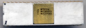
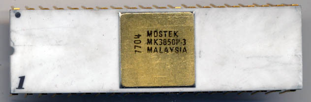
Mostek MK3850P-3 – F8 Processor – 1977

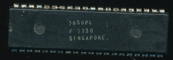
In September 1974 Fairchild Camera and Instrument’s Fairchild Semiconductor division announced they were throwing their hat into the microcontroller market.  The same Fairchild whom created ‘Silicon Valley’ whom many of the ‘greats’ of the industry originally worked, including Gordon Moore, and Robert Noyce, of Intel fame.   In April 1975 Fairchild began sampling the F8 processor with production quantities available in the fall of 1975.

Fairchild knew the importance of having second sources available and in June 1975 reached an agreement with Mostek to allow Mostek to produce the F8 as well.  The 10 year agreement with Mostek included complete mask set transfers as Mosteks NMOS isoplanar process was completely compatible with Fairchilds.  The agreement also called for continuing development of the F8 processor system, allowing each company to develop F8 products independently of each other as well as together (this is important down the road).

Fairchild 3850PC - 1977

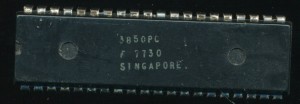
Fairchild 3850PC – 1977

Mostek was able to rapidly produce the F8 system, faster, cheaper, and more reliable than Fairchild.  The F8 introduction price was $130 per unit.  When Mostek began production in 1975 prices were down to $85 per unit.  In February 1976 Mostek lowered prices to $55 per unit ($64 to $28 if you bought more than 100 pieces).  The F8 was also licensed to SGS-Ates of Italy in 1976.

Also in February of 1976 Fairchild signed a agreement with Olympia Werke A.G., a German company, allowing production and sharing of information on the F8 processor.  It also allowed Fairchild (and any of its second sources, including Mostek) to use any of Olympia’s processor technology and products. So why did Fairchild reach such an agreement with Olympia, a relatively small company?  Because General Instruments was suing Fairchild at the time.

AEG Telefunken U3870M - F8 Processor

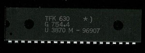
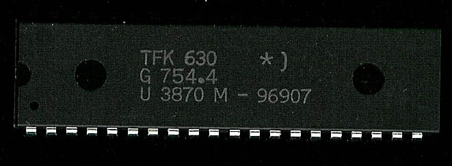
AEG Telefunken U3870M – F8 Processor

It gets a little messy here but try to follow along. A man named Dr David Chung (head of GI’s microprocessor division) was dispatched to Olympia to pick up some proprietary information on a top secret 8-bit processor Olympia was developing called the CP 3-F.  GI had an agreement to license this processor technology from Olympia and it was Chung’s job to get the information to make that possible.  Very shortly after Chung’s return from Germany he quit GI.  Who hired him? Fairchild of course.  GI accused Fairchild (and Chung) of using the proprietary information on the CP 3-F to develop the F8 processor.  By reaching an agreement with Olympia, Fairchild now was legally covered if in fact they HAD used information on the CP 3-F in the design of the F8.  Unfortunately very little information exists on the CP 3-F but it is widely believed that it was the basis of the Fairchild F8.

Updated with new info from comments 07/17/2021

The CP 3-F was a 4 chip design, very similar to the F8, with a CPU/Control Chip (RSE), a ROM (Program Storage Unit) RAM (Data Storage Unit) and an I/O Chip.  The CPU supported 48 8-byte instructions and has a 48 byte RAM.  The PSE was a 1024x 8 bit ROM and the DSE contained a 128 x 8 bit RAM, the address register, and an 8-bit I/O channel. They were all made using a PMOS process (needing -5V and -17V) and packaged in 40 pin DIPS.  They used an 800KHz clock which was internally divided by 4 resulting in a internal 200KHz (5 microsecond) cycle time.

Its clear that perhaps the general idea of the CP 3-F was used, but it was updated and expanded (switched to NMOS, new instructions added, faster, etc)

The court case went on into the 1980’s by which time it didn’t really matter.  I was unable to determine who ‘won’ but by production dates of the F8, it didn’t matter one way or another.

So what about the processor?
Read More »