DEC NVAX++ NV5: The End of VAX
About a year ago we covered the DEC RIGEL VAX Processor. After The RIGEL DEC moved to make a single chip VAX processor that would include the CPU, FPU, and cache controller on one single die. Work on the design began in 1987, and first silicon shipping in 1991. Performance ended up being as good or better then the very high end VAX 9000 systems (implemented in ECL logic).
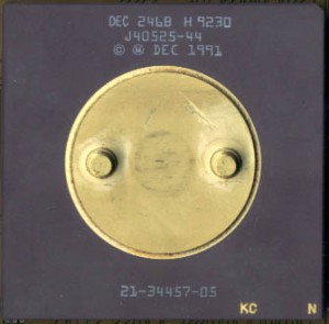
The original NVAX processor was made on a 0.75u 3-Layer CMOS process (DEC CMOS-4) and contained 1.3 million transistors in a 339 pin CPGA package. Initial clock speed, in 1991 was 71MHz. NVAX was then the fastest CISC processor made. Speeds ramped up to 90.9MHz at the high end and a lower end of 62.5MHz. The first NVAX models were identified as 246B and 246C. Later versions, made well into 1996, were made on the CMOS-4S process, a 10% shrink to 0.675u and were labeled 1001C.
Internally NVAX was very familiar, the FPU was largely reused directly from RIGEL. The NVAX also maintains the 4-phase clocking scheme from RIGEL, but moves the clock generator on chip. It also maintained the 2K of on die instruction cache from RIGEL, but added a 8K data/instruction mixed cache as well. An L2 cache was supported in sizes of 256K 512K 1M or 2M, and located off chip. The NVAX continued the 6-stage pipeline of RIGEL with some enhancements. One of the greatest performance enhancements over RIGEL is the handling of pipeline stalls. In the RIGEL pipeline, a stall in one stage would stall the entire pipe line, whereas on NVAX, in most cases, a stall in one stage does not prevent the other stages from continuing.
At nearly the same time as the development of the NVAX DEC was also developing a competitor to MIPS, a RISC architecture. This new RISC architecture was codenamed EVAX, for Enhanced VAX, and was a purely RISC architecture that could run translated VAX CISC code with very little performance penalty. It did however borrow from VAX, like the NVAX, EVAX used the FPU from the RIGEL. DEC went on to brand the EVAX as Alpha AXP, to separate it from the VAX line, though its internal naming of EV4, EV5 etc was left intact, as the last remnant of VAX.
Having two high performance processor types at the same time left DEC in a bit of a dilemma so they created a third, known as the NVAX+ (DEC 262D). The NVAX+ was originally made on the same CMOS-4 process as the NVAX and ran at 90.9MHz. The NVAX+ was meant to be a bridge between the VAX line and the Alpha AXP. It was a NVAX core, wrapped in an EVAX (Alpha AXP) external interface, it was made in the same 431PGA as the Alpha 21064 and was pin for pin compatible, the same board could be used for either. It supported more L2 cache then the NVAX, supporting six cache sizes (4MB, 2MB, 1MB, 512KB, 256KB, 128KB),
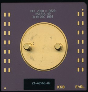
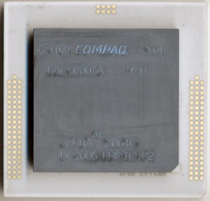
In 1994 the NVAX+ was shrunk to the DEC CMOS-5 4-Layer 0.5 micron process resulting in the NVAX++ (DEC 299D) which ran from 133-170.9MHz. These speeds continued to be the fastest CISC processors until Intel released the Pentium Pro at 180 and 200MHz in 1996. Ultimately Intel’s dominance, and the coming dominance of RISC performance were the writing on the wall, and the VAX, and not long after it DEC itself were doomed to reside in the history books. By 1997 The NVAX++ was off the market. In 1997 the DEC Alpha team was operating out of offices owned by Intel (who also took over DEC’s fab’s), and in 1998 the remains of DEC, and the Alpha team, were bought by Compaq. And by 2004 Alpha was phased out in favor of Itanium (a now rather ironic decision by HP/Compaq).
Posted in:
CPU of the Day


