
CPU of the Day: Fairchild F8 Microprocessor
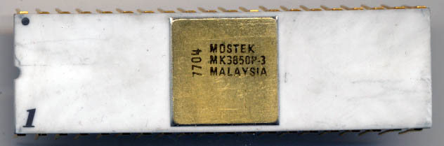
Mostek MK3850P-3 – F8 Processor – 1977
In September 1974 Fairchild Camera and Instrument’s Fairchild Semiconductor division announced they were throwing their hat into the microcontroller market. The same Fairchild whom created ‘Silicon Valley’ whom many of the ‘greats’ of the industry originally worked, including Gordon Moore, and Robert Noyce, of Intel fame. In April 1975 Fairchild began sampling the F8 processor with production quantities available in the fall of 1975.
Fairchild knew the importance of having second sources available and in June 1975 reached an agreement with Mostek to allow Mostek to produce the F8 as well. The 10 year agreement with Mostek included complete mask set transfers as Mosteks NMOS isoplanar process was completely compatible with Fairchilds. The agreement also called for continuing development of the F8 processor system, allowing each company to develop F8 products independently of each other as well as together (this is important down the road).
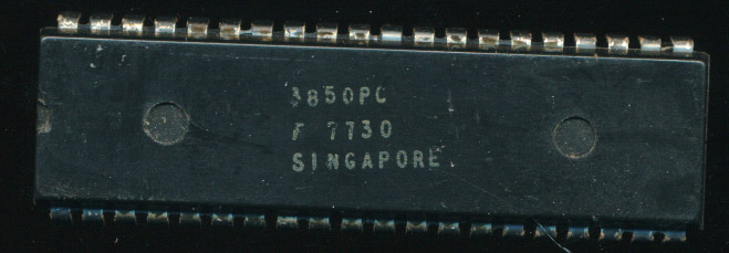
Fairchild 3850PC – 1977
Mostek was able to rapidly produce the F8 system, faster, cheaper, and more reliable than Fairchild. The F8 introduction price was $130 per unit. When Mostek began production in 1975 prices were down to $85 per unit. In February 1976 Mostek lowered prices to $55 per unit ($64 to $28 if you bought more than 100 pieces). The F8 was also licensed to SGS-Ates of Italy in 1976.
Also in February of 1976 Fairchild signed a agreement with Olympia Werke A.G., a German company, allowing production and sharing of information on the F8 processor. It also allowed Fairchild (and any of its second sources, including Mostek) to use any of Olympia’s processor technology and products. So why did Fairchild reach such an agreement with Olympia, a relatively small company? Because General Instruments was suing Fairchild at the time.
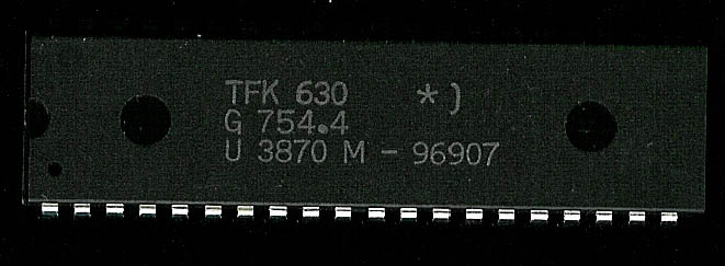
AEG Telefunken U3870M – F8 Processor
It gets a little messy here but try to follow along. A man named Dr David Chung (head of GI’s microprocessor division) was dispatched to Olympia to pick up some proprietary information on a top secret 8-bit processor Olympia was developing called the CP 3-F. GI had an agreement to license this processor technology from Olympia and it was Chung’s job to get the information to make that possible. Very shortly after Chung’s return from Germany he quit GI. Who hired him? Fairchild of course. GI accused Fairchild (and Chung) of using the proprietary information on the CP 3-F to develop the F8 processor. By reaching an agreement with Olympia, Fairchild now was legally covered if in fact they HAD used information on the CP 3-F in the design of the F8. Unfortunately very little information exists on the CP 3-F but it is widely believed that it was the basis of the Fairchild F8.
Updated with new info from comments 07/17/2021
The CP 3-F was a 4 chip design, very similar to the F8, with a CPU/Control Chip (RSE), a ROM (Program Storage Unit) RAM (Data Storage Unit) and an I/O Chip. The CPU supported 48 8-byte instructions and has a 48 byte RAM. The PSE was a 1024x 8 bit ROM and the DSE contained a 128 x 8 bit RAM, the address register, and an 8-bit I/O channel. They were all made using a PMOS process (needing -5V and -17V) and packaged in 40 pin DIPS. They used an 800KHz clock which was internally divided by 4 resulting in a internal 200KHz (5 microsecond) cycle time.
Its clear that perhaps the general idea of the CP 3-F was used, but it was updated and expanded (switched to NMOS, new instructions added, faster, etc)
The court case went on into the 1980’s by which time it didn’t really matter. I was unable to determine who ‘won’ but by production dates of the F8, it didn’t matter one way or another.
So what about the processor?
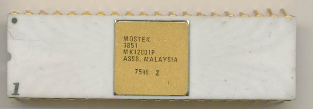
Mostek 3851 MK12001P Program Storage Unit from late 1975
The F8 was a 2 chip microcontroller. It consisted of (at a minimum) a 3850 CPU and a 3851 PSU (Program Storage Unit). The CPU includes 64 bytes of RAM and the ALU. It was made on a NMOS isoplanar process and ran at 1-2MHz. It contained 76 basic instructions. The PSU includes 1K of ROM for program storage, as well as the program counter (PC), Stack Pointer, and Data Counter. I/O was handled by the CPU, while memory access was handled by the PSU. It was an ‘odd’ design at its time but it had a profound impact on the industry. At the time processors were designed one function per chip. The F8 integrated all functions needed by the processor system onto 2 chips. Even the clock driver, which historically had been its own device, was part of the 3850 CPU. The system could be extended by adding more 3851s or 3852/3 memory interface chips (for DRAM and/or SRAM). In addition to the 3851 PSU there was also enhanced versions with more ROM and additional timer controls called the 3856 and 3857.
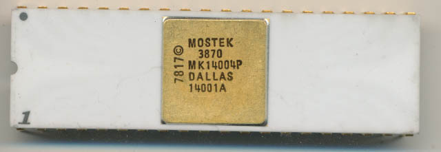
Mostek 3870 MK14004P – 1978 – Single chip F8
After the F8 almost every single microcontroller included all these function on one chip. The Intel MCS-48 was very similar to a single chip implementation of the F8.
As processes improved it became possible to integrate the F3850 and F3851 onto a single chip, forming a single chip microcontroller called the F3859. The 3859 is extremely rare because Mostek, who was developing their own single chip implementation of the F8 released the 3870 series. Once the 3870 hit the market, the 3859 was canceled.
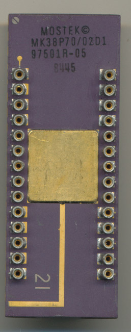
Mostek MK38P70-02D1 – Piggyback
The Mostek 3870 was a greatly enhanced F8. It is essentially a 3850 CPU with a 3856 PSU with some further enhancements. The 3870 also includes 64 bytes of executable RAM and runs on a single 5V supply (the 3850 requires 5 and 12V supplies). It is also slightly faster, 1.5usec cycle time (using a 1-4MHz clock) versus 2usec for the 3850. In addition is was cheaper to make, much cheaper. On the 3859 (and 3851) the customers ROM mask was implemented early in the manufacturing process. This results in a much higher mask charge, $10,000-$15,000. Mostek reworked the design such that the Mask layer was the last layer implemented. This means it can be done much more inexpensively (with better known yields). Mask charges for a 3870 were close to $1000. Ironically Fairchild second sourced the Mostek 3870 (as originally agreed upon by their licensing agreement).
The 3870 went on to be made in many versions, different amounts of RAM, ROM, and packages, including a development package that had a socket on top for an EPROM. The 3870 was also made by Telefunken whose parent company was AEG (of Germany). AEG is also the parent company of Olympia Werke, whom developed the C3PF processor that the F8 was based upon. When Mostek was merged with ST Microelectronics, ST continued making the 3870 series, well into the 1990’s. Fairchild made the 3850 into the mid 1980’s before it was discontinued when National Semiconductor bought Fairchild.
Its legacy has survived however. Microcontrollers today continue to integrate more and more onto the same chip, Flash, RAM, ADCs, DACs, high voltage drivers for displays, and arrays of counters and timers. Certainly this was a natural evolution of the microcontroller but it was the Fairchild F8 that began that evolution.
June 29th, 2013 at 1:37 pm
I like the 3870/F8 architecture. It’s limited in some ways but overall it’s pretty cool and the piggybacks are really fun to use, it’s flexible enough that it allows both reading and writing to the external program memory. The executable on chip RAM is quite interesting feature too and I think pretty unusual at the time (or is it?). The integrated timer/counter is basic but it became the standard on any later microcontrollers.
June 14th, 2014 at 3:09 pm
[…] ένα μοντέλο επίδειξης του 8μπιτου επεξεργαστή F8. Αν και ο πιο σωστός όρος για το F8 είναι chipset, καθώς το […]
November 27th, 2014 at 3:59 am
i have read about fairchild f8 history, but it seem this article give me more history. could i make this article as reference on my paper?
November 27th, 2014 at 10:31 am
No problem
-John
February 29th, 2016 at 7:34 am
Great article on an interesting cpu. Wonder what happened that they didn’t evolve this like 8008 to 8088 etc.
March 1st, 2016 at 6:47 pm
That’s a great question, in some ways it lives on in the Intel MCS-48, which is similar to it in many ways.
April 26th, 2017 at 7:30 pm
would like to find some one who could advise me how to recover the data in mostek micro
thnks ron hathcock
rjhath1950@gmail.com
December 25th, 2017 at 2:42 pm
I have recovered several of these Mostek components. Is there are market for them now? Should I proceed to sell them via eBay etc. or just recycle them to my refiner?
Thank YOU
December 28th, 2017 at 5:16 pm
They probably would sell ok on eBay. Let me know what ones you have, maybe some i need,
January 13th, 2020 at 1:53 am
“Wonder what happened that they didn’t evolve this like 8008 to 8088 etc.”
No more Olympia IP to steal? (snark)
August 17th, 2021 at 12:04 pm
The “Olympia-werke” CPU name is CP3F (not C3PF), with a searchmachine
then able to find bit more info in german language only about this CPU – e.g:
http://www.simulationsraum.de/wp-content/uploads/SimRaum-Downloads/%C2%B5P1%20-%20Hardware.pdf
-> Page 48
August 17th, 2021 at 8:39 pm
Thank you, I fixed the CP3F naming and added more info from the document you provided. Thanks for taking the time to let me know.
December 31st, 2021 at 11:19 am
I have somewhere a 3 chip F8 evaluation board. As I recall, the 3rd chip did not have the interrupt input, which meant you couldn’t swap memory. I may be wrong about this. Fairchild also had an early video game out that used the F8. BTW, the evaluation board came with a cross compiler on Hollerith cards!
March 13th, 2022 at 4:47 pm
Marvin, are you considering selling the development board?
April 10th, 2022 at 4:47 am
Hi, after some CP3F reseach – I found two articles:
(only available in german language)
http://www.simulationsraum.de/wp-content/uploads/SimRaum-Downloads/%C2%B5P1%20-%20Hardware.pdf
and
https://nvhrbiblio.nl/biblio/tijdschrift/Funktechnik/1976/FT_1976_Heft_12_OCR.pdf
They describe the CP3-F/CP3F a little, so I came to the conclusion that the
CP3F and the SGS-Ates M380 and the General Instruments LP8000
are the same processors: Olympia had no chip-Fab so SGS and GI made them
but with different names! So your webside has already some a page about the
CP3F aka M380 or LP8000:
https://www.cpushack.com/2014/10/30/sgs-ates-m380-and-gi-lp8000-8-bits-for-europe/
May 14th, 2023 at 1:06 pm
Two of the Mostek 3870 CPUs are used on the base boards of the first portable electronic daisywheel typewriter of the world, the 1980 made Olivetti Praxis 30 and Praxis 35 and it’s successors Praxis 40, Praxis 41 and Praxis 45D. The Praxis 30 is also known as the Underwood 3000.
May 14th, 2023 at 1:13 pm
Here is a link to the typewriter and it’s CPU: https://forum.classic-computing.de/forum/index.php?thread/26804-golem-de-als-deutschland-eine-eigene-cpu-hatte-olympia-cp3-f/&postID=349061#post349061
August 11th, 2023 at 11:15 pm
In late 1976, Bally produced a solid-state home pinball game. This was marketed under a few different titles, but it was always the same game, with only the artwork package being different. The control board for this game was built using a 3850 CPU supported by two 3851 PSUs. These machines had full-sized playfields, although the game play was fairly simple. They were sold directly into the home market via catalogs such as Wards and JS&A Sales for around $800. There was even a Heath-Kit version for around $600. These machines can still be found in homes today, handed down to the children of the original owners. More information about this game can be found on the Internet Pinball Database: https://www.ipdb.org/machine.cgi?id=4116
March 3rd, 2024 at 5:00 pm
Tim, I have read that there was also a series 2 that used the Mostek 3870. Someone commented in one of the topics about them that both the series 1 and the series 2 had serious design flaws, related mainly to a lack of protection for the +5v. The power supply, as I recall reading, would over-volt and fry the chips. According to the comment, the series 2 machines have protections added but not for the most critical part (the +5v). I have no electrical knowledge so I am just repeating what I read. It’s interesting that a company would be able to design such a sophisticated board but wouldn’t bother, even on the revision, to implement the most important protection for the chipset.