The History of the SUPER HEDT x86 PC
Introduction
 Last time we talked about the history of the development of high-end computers or High-End Desktop PC (HEDT). In the discussion of the article, some readers remembered motherboards that belonged to HEDT, but were one step higher, both in terms of their technical characteristics and in terms of the cost of ownership of the entire platform based on them. It is possible to name such very high-performance systems – Super HEDT, which often also had their own personal names, and we will talk about them this time.
Last time, the date of the appearance of Intel processors for LGA1366 and the announcement of the first motherboards for them was taken as the beginning of the countdown for the announcement of the HEDT platform. This event happened in the fall of 2008. The reason for the appearance of such platforms was dictated by the decision of the main chipmaker to create two platforms: one for all consumers, and the second specifically for enthusiasts who are ready to get additional performance and new features for extra money that were not available (or needed) for owners of conventional desktop platforms. The logic of making such a decision is simple and logical, but with Super HEDT platforms things are somewhat different.
 There may be several reasons for the emergence of such platforms. One of which is to show a competitor that we can do even it better and even faster, to make performance extremes, at the cost of incredible efforts of engineers and, as a result, an incredibly high final price for the end user. Although, for such systems, the price, although it plays an important role, is not a deterrent, because there will always be enthusiasts who are willing to pay as much as the manufacturer dictates to have the very best.
By announcing such a platform, the manufacturer can be sure that the fame and success of his Super HEDT platform will smoothly spill over to his other products, even in the budget segment, because if he is capable of producing a Super “miracle” of engineering, then all of his products, will also have the same properties as the miracle ones, only they will be slower performance and a reasonable price. Super HEDT aura and advertising will do their job and competitors will be forced to return from heaven to earth, because they will have nothing to answer.
 The second reason for the appearance of such systems may be for a diametrically opposite reason – when the manufacturer fails to defeat a competitor on his football field and the only way out is to continue the game somewhere in the orbit of the planet, where the opponent will definitely not fly. Your own personal field – your own rules, even if the price of such a decision will also be cosmically high and beyond the reach of most earthlings. But they will talk about such a decision, though not for long, but long enough to lift you up onto the podium of media fame for a brief time..
And oddly enough, the first Super HEDT system recalled in this article will be the system that was born according to the second, more pessimistic scenario. Has anyone already guessed it?
To find the answer to this question, we will have to go back in time to the very end of November 2006. At this time, the golden years of AMD had already passed, the dominance of its extremely successful Socket 939 and the fastest single-core processors, which included the various Athlon 64 FX’s, had ended. With the introduction of new revolutionary Intel Core processors to the market, AMD had been cornered with its Socket AM2. The market turned towards multi-core, and AMD had nothing to boast of in performance per core. The appearance of the first quad-core Intel Core 2 Quad processors completely deprived AMD of any chance for worthy competition.
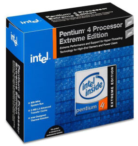
 If you look at the range of processors available on the market in the fall of 2006, AMD had different Athlon 64 X2’s, manufactured according on a rather outdated 90 nm process technology, the fastest model was the Athlon 64 X2, 5200+ with a real clock speed of 2.6 GHz and a processor for ” green” enthusiasts, the Athlon 64 FX-62 with a clock frequency of 2.8 GHz and a recommended price of $1031. At this time, Intel was selling the Core 2 Duo E6700 with a clock frequency of 2.66 GHz and a recommended price of $530 and a dual-core flagship Core 2 Extreme X6800 at 2.93 GHz, 1066 MHz FSB and 4MB of L2 cache. The cost of all Extreme Editions then was $999. But in November, Intel got its first 4-core processors based on the “Kentsfield” core. The Intel Core 2 Extreme QX6700 was clocked at 2.66 GHz and became the first halo chip, and then more “popular” models followed to conquer the market. The “Kentsfield” core itself was not an honest “quad-core”, it consisted of two Core 2 Duo cores placed on the same substrate. (Hello to all chiplets, and a separate AMD Ryzen) Well, AMD did not go well with its Phenoms, but something had to be done, at least for the sake of media noise.
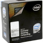
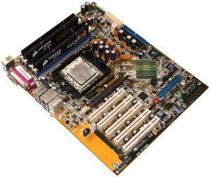
Core 2 Extreme X6800
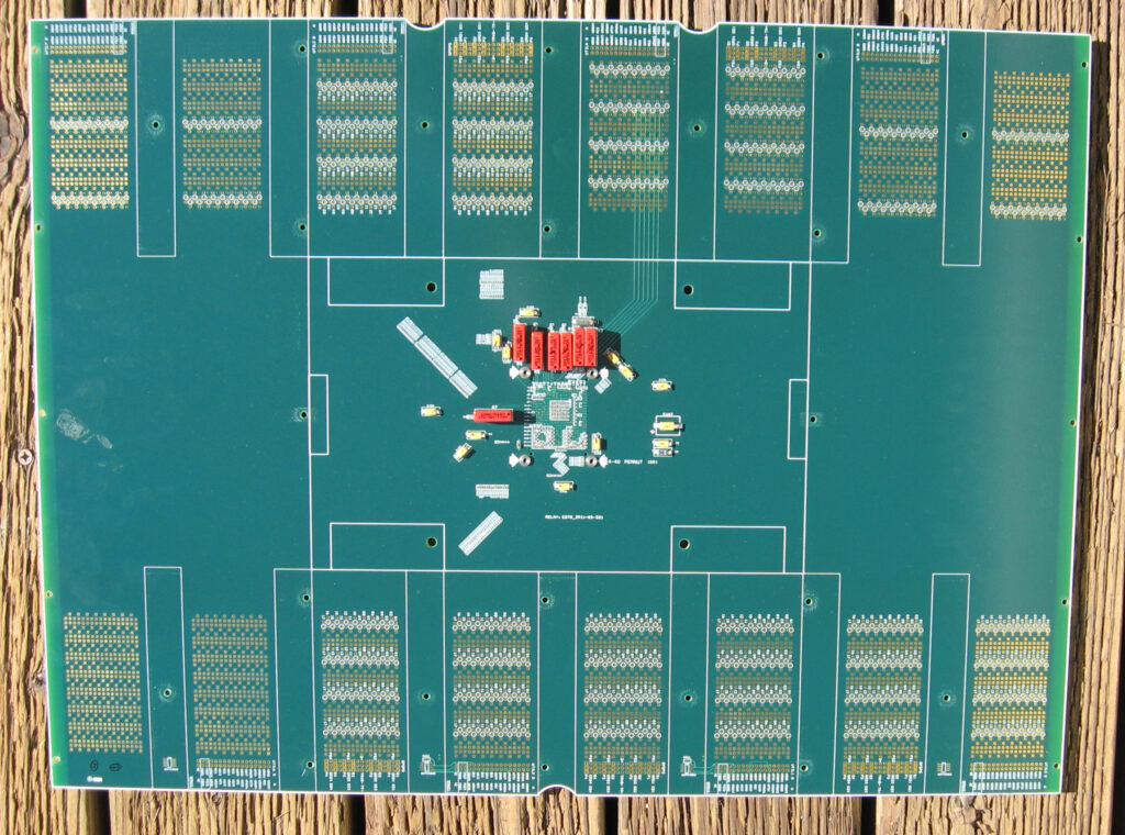
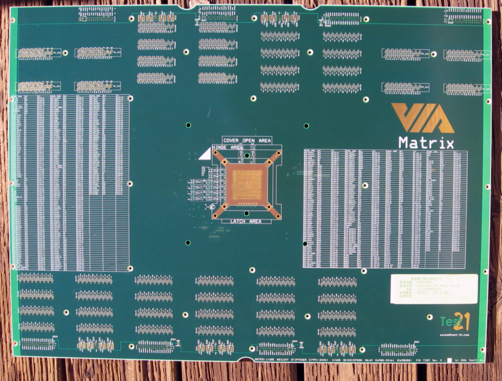
The recipe for such an answer is always the same: let’s take our server platform, embellish it a little, adapt the BIOS for enthusiasts, and give the server processor a free multiplier. We will make the number of sockets more than one and the answer is ready. But server systems have a lot of limitations, besides, some of them are hardware-based and cannot be adapted to desktop standards. But in such cases, there is no time for compromises, it is better to sacrifice functionality, performance will not suffer much from this.