November 20th, 2021 ~ by admin

The Soviet 1801VM3 Enhanced LSI-11 Processor

This is turning into a bit of a series on Soviet processors.  Continuing from our article earlier on the 1801VM2 LSI-11.  The 1801VM3 is the further development of 1801VM1/VM2 and is the highest performance microprocessor in 1801 series. It’s a 16-bit single-chip microprocessor that includes an operating unit, a firmware control unit, an interrupt unit, a memory controller and Q-BUS control unit. A distinctive feature of 1801VM3 is a large amount of addressable memory (4MB vs 64K for the 1801VM1 and 64k+64K for the VM2), high performance and ability to connect a floating-point coprocessor 1801VM4.

1801VM2 die

1801VM3 Die

1801VM3 Specifications

  • Number of processor Instruction: 72 Fixed Point and 46 Floating Point (with 1801VM4 FPU)
  • Address Space: 4MB
  • General Purpose Registers: 8
  • Manufacturing process: 4 micron N-channel silicon gate MOS technology (later migrated to 3 micron)
  • Die size 6.65 × 8 mm
  • Transistor count: 28,900 active transistors, 200,000 integral elements
  • Clock rate: 4MHz  (1801VM3V) 5MHz (1801VM3B) 6MHz (1801VM3A, upgraded to 8 in 1991)
  • Performance: For register based operations (like addition) up to 1,500,000 instruction/s (1.5 MIPS)
  • IRQ Lines: 4
  • Supply voltage + 4.75V-5.52V
  • Power consumption: 1.7-2 W
  • Packages: CDIP64 (KM1801VM3) LQFP64 (KA1801VM3) CQFP64 (KN1801VM3/N1801VM3)

Like the VM2 before it the speeds were denoted by a series of dots on the package (or lack thereof)

KM1801VM3A – 6MHz (no extra dot) CDIP64 package from 9008

KM1801VM3B – 5MHz (one extra dot) CDIP64 package from 9003

KM1801VM3V – 4MHz (two extra dots) CDIP64 package from 9202


KA1801VM3 – 8MHz (no extra dot – post 1991) PQFP64 package from 9108

N1801VM3 – 8MHz (no extra dot – post 1991) CQFP64 package from 9324 – Remarked from a military part (rhombus marking marked over)


The KM1801VM3 appeared as part of the DVK line of computers, starting with the DVK-3M model (PCB ”Electronics МС 1201.03” and “Electronics МС 1201.04”).  Using the same ISA (Instruction Set Architecture) allowed DVK (and others) to rapidly update their computer line when new processors were available, and allow for a wider software base.  This is very much like the original IBM PC using the x86 architecture.  The transition from 8086 to 80286 was relatively easy to design, and nearly seamless for the end user.

DVK PCB Electronics МС 1201.03 board on the top.

Many devices built on the basis of the 1801 series CPU contain other microcircuits of the same series (support circuits).
In addition to microprocessors, this series includes:
– ULA 1801VP1-xxx
– masked ROM 1801REх-xxx
– EEPROM 1801RR1

ULA and EEPROM

The 1801VP1-xxx is a ULA- (Uncommitted Logic Arrays). It’s made using a 3 micron N-channel silicon gate MOS technology with one metal layer. First, base silicon wafers are made that contain transistors. These are doped regions of silicon and a separate oxide-insulated layer of polysilicon gates. Then all this is covered with an oxide layer. Base wafers are ready.

In this form, the wafers can be stored for a long time or transferred to another fab. All 1801VP1-xxx chips, regardless of number, have the same structure and arrangement of transistors. And they are made on the same base wafers.

KR1801VP1-22 die

Differences between the chips appear only at the last stage of manufacturing. In the upper oxide layer, the die is etched by photolithography to access the required transistors. And then form a metallic pattern from aluminum. This pattern defines the electrical circuit. The number in the marking identifies the purpose of the chip. For example, 1801VP1-033 is an external device controller.  This is similar to how a MaskROM is made but instead of only memory elements, it contains logic elements allowing for a custom IC to be made (like a mask programmable PAL/GAL)

KR1801VP1-119

The 1801VP1-119 is a companion chip for 1801VM3. It can be said to be the “north bridge“.
The 1801VP1-119 performs the following functions:
-forms control signals for DRAM;
-forms control signals for system SRAM;
-generates signals to select system ROM;
-generates control signals for detection and correction of memory errors (EDC) using Hamming code (555VGH1). Error correction circuits reduced performance by 10-15%. Therefore in some computers, there were jumpers to enable/disable the EDC
-buffer data register control;
-generate other signals

This was the beginning of what would be come chipsets, replacing loads of TTL with custom circuits.  The exact same evolution was occurring in the west with the PC environment, until nearly all the support circuits were integrated into just a couple large ASICs.   Its interesting to see the development paths of the Soviet computers and the West.  While they were entirely different instruction sets, they evolved in very much the same way.  East or West, LSI-11 or x86, at the end of the day, a computer is a computer and will evolve in similar fashion.


Posted in:
CPU of the Day

November 4th, 2021 ~ by admin

The Soviet 1801VM2 LSI-11 Processor

The Soviet-made 1801VM2 CPU (a binary-compatible implementation of the PDP11 instruction set and QBUS interface) was developed in 1982. The 1801VM2 is a further development of the earlier 1801VM1 doubling the original 5MHz clock speed. From a constructive standpoint this CPU is a completely independent development.

1801VM2 die

1801VM2 die – 1983 dated

1801VM2 Specifications

  • Number of processor Instruction: 72
  • Manufacturing process: 4 micron N-channel silicon gate MOS technology
  • Die size 5.3 × 5.35 mm
  • Transistor count: 18,500 active transistors, 120,000 integral elements
  • Clock rate: Up to 10 MHz
  • Performance: For register based operations (like addition) up to 1,000,000 instruction/s (1 MIPS) – for operations like multiplication, up to 100,000 instructions/s
  • Supply voltage + 5V
  • Power consumption: up to 1.7 W
  • The case is 40-lead, ceramic DIP (KM1801VM2) or plastic DIP (KR1801VM2). (a surface mount version was also made)

To increase noise immunity in comparison with 1801VM1, additional ground contacts were made for the address / data bus.
The 1801VM2 was manufactured at two factories: Angstrem and Solnechnogorsk Electromechanical Plant (SEMZ).  As was typical of the time speed grading was done by adding extra marking to the chips post-testing.  Its very easy to miss these, if a chip was tested at 10MHz and passed it received no extra marking and was considered an 1801VM’A.’  If the device failed at 10MHz but ran at 8MHz a small dot was added to the package (and was considered a grade ‘B’ device).  This dot was not to be confused with the dot for the pin one marker, though often placed…next to it.

Ceramic DIP 1801VM2A Angstrem – 1989 No extra dot

Ceramic DIP 1801VM2B Angstrem – 1987 – Note the extra dot in this case by the date code

Plastic DIP 1801VM2A Angstrem – 1990

KN1801VM2- Angstrem 1985 CQFP Surface mount version (image Baator)

Ceramic DIP 1801VM2 Solnechnogorsk Electromechanical Plant – 1990 – Extra dot by pin 1 marker

In comparison with 1801VM1, expanded arithmetic instructions (MUL, DIV, ASH, ASHC – part of a the set of PDP-11 EIS), and also operations from the floating point instruction set (FIS) were added. The FIS instructions (FADD, FSUB, FMUL, FDIV) are realized through subroutines – when performing these instructions there is a special type of interrupt and the program handler in memory (“shadow” system ROM K1801RE2) of the console mode is executed, a ‘firmware’ style of FIS implementation, as its not truly hardware (the ROMs break down the FIS instructions into something the 1801VM2 can execute)
During the design of the microprocessor, a microcode error was made, leading to a malfunction of the processor when reading with addressing method 17 ( MOV (PC), R0).

DVK-1 Computer

The 1801VM2 was the heart of a number models of DVK computer. DVK was developed at the Research Institute of Precision Technology , Zelenograd (just outside of Moscow). The first model DVK-1 was developed in 1981, and released in 1983. Architecturally DVK copies mini-computers from DEC PDC-11 and PDP-11. By 1990, 200,000 DVK computers of the nine different models were produced.

Romashka Word Processor

Use of the processor continued well into the 1990’s. The “Romashka” belonged to the latest generation of electronic typewriters, which in their functionality were close to computer text editors. This typewriter made it possible to automatically format text (set alignment, change the spacing between characters and between lines, use bold and underlined fonts, etc.) and had an electronic memory of at least one page (3800 bytes).  In the West these half typewriter half computer were called Word Processors, and were quite popular through the 1980’s.   The machine’s control unit was a microcomputer based on the KM1801VM2 processor.
“Romashka” was produced by the Kursk PO “Schetmash” in the first half of the 1990s.

“Electronics IM-05 “- Soviet chess computer, contains 1801VM2 inside. It was a continuation of the line of chess computers “Electronics”. Produced by the Svetlana Association, Leningrad.

In 1984, the military-grade microprocessor 1806VM2 was released.
This microprocessor functionally corresponds to the 1801VM2, but is made using CMOS technology.

  • Clock rate: up to 5 MHz
  • Number of Instructions: 77
  • Contains 134,636 integral elements
  • Power consumption: up to 0.025W

The 1806VM2 developers fixed the microcode bug present in 1801VM2 (much to the relief, or annoyance of programmers). The 1806VM2 was supplied in a 42-lead dual in-line ceramic package with flat leads, N1806VM2 in a 64-lead CQFP. The rhombus marking on the chips denotes a military-grade device.

1806VM2 – Angstrem 1991 in the nice pink flat pack

N1806VM2 – Angstrem 1999 in a Ceramic quad flat pack

CQFP N1806BM2 on a ceramic substrate forming a military Single Board Computer – circa 1987 (image Baator)

These 1806VM2 are still being made by Angstrem, if you need to build a PDP-11 computer to run Tetris on, or repair a Buran shuttle you may have laying around.

In 1990, a radiation-hardened microprocessor was introduced, compatible with the 1806VM2, known as the 1836VM2/N1836VM2.  Just like in other countries, existing code base and known reliability are more of a driver of what the military/industry uses than having the latest and greatest.  There are still MIL-STD-1750A processors being made and used, rad-hard 8051s and 80186s, and Soviet PDP-11 processors right there with them.

Photos of microprocessors from the collection of Perfiliev Andrey (Andreycpu).
Article written originally by Contributing Author Vladimir Yakovlev (edited by cpushack)

Posted in:
CPU of the Day

October 22nd, 2021 ~ by admin

The IBM 4020 Military Computer – Tracking Missiles with 6-bit Bytes

IBM 4020 Q-Pacs – 1960’s

Back in the late 1950’s two things were happening (ok more then 2 but 2 relevant to todays discussion) the military was looking to replace the new but now already out of date tube based SAGE and AN/FSQ-7 Strategic Air Command (SAC) computers, and multiple bits of data were beginning to be called bytes.  The SAC was in charge of all of the US’s Strategic bombers, ICBMs, and detecting/tracking the threats of bombers/ICBMs from the USSR.  The older tube based SAGE computer was designed for relaying, consolidating, and displaying data from Early Warning RADARs across North America to paint a situation picture of what was going on.  It worked fine, for bombers, but the late 1950’s also brought about ICBMs, and ICBMs are much much faster then mere bombers.  The SAGE, and the AN/FSQ-7 lacked the processing speed to keep up with the changing data from a RADAR track of an ICBM so something faster was needed.

Each module weighs around 90 grams

IBM developed and proposed the AN/FSQ-31 (and the FSQ-7A which got renamed the FSQ-32) which were based on the newly developed IBM 4020 military computer.  The IBM 4020 was completely transistor based and designed for reliability and speed.  Marketing materials of the time refer to its ‘resistance to the effects of nuclear blast,’ clearly this was the 1950’s.  At the heart of the 4020 designs was the Q-Pac. These were pluggable, ceramic encapsulated circuit packages. The majority of all logic requirements can be met
by seven basic types of Q-Pacs, each containing from one to four circuits. The use of transistors, diodes, and resistors/caps on each Q-Pac served as what TTL/RTL of the 1960’s/1970’s formed, discrete logic elements, albeit simple ones. In the 4020 the computer was divided into modules (racks) which each contained 16 drawers. Each drawer could hold 96 individual Q-Pac (or 48 double Q-pacs).  That’s 1536 logic elements per module, and the 4020 had 8 modules, resulting in around 12,288 Q-Pacs.  It appears each Q-pac could support 6 discrete transistors, so the 4020’s basic data path (not counting memory, I/O or storage subsystems would max out at 73k transistors.  Obviously there would not be a system that was ALL transistors but this gives us an idea of the scale of the computer. This is around what the Motorola 68000 CPU had or a Intel 80186.  The typical 4020 (again not counting the peripherals) was water cooled, used 13kw of power and took a good 85 sq ft of floor space.

Five simple transistors in the one on the left, and a pair of diodes on the right.

The 4020 was a 48-bit word length (pus 2 parity bits) computer and was capable of around 400,000 Instructions per second with a 2.5microsecond cycle time (6.25MHz).  It supported 128kwords of drum storage (remember 48 bit words, so this is about 6Mbit.  The 4020 also supported byte processing, using the 48-bit word as 8 6-bit sections which IBM called bytes.  This is one of the first official commercial usages of the term ‘byte’ for a chunk of data.  We think of bytes as 8-bits but thats only a standard thats been around the last 30 years or so.  Back in the 1950’s it was the wild west of data naming.  It was common to use 6-bits for BCD (Binary coded Decimal) and 6-bits to represent characters, so a 6-bit byte was only natural for IBM to use.  This eventually gave way to the 8-bit bytes we all know and love by the late 1960’s, though some processors even in the 1970’s used 12-bit words (Intersil 6100 and some PICs) and other oddities (14 bits from the PIC16).

AN/FSQ-31

The process of integrating the 4020’s into SAC facilities took longer then expected, not being completed until 1968, by which time they were of course outdated again.  By 1975 most of them had been replaced by newer Honeywell systems.  Interestingly, the 4020’s tube driven predecessor lasted in some bases until the early 1980’s.

It wouldn’t surprise me if, even after 60+ years, these Q-Pac modules still worked, after all, that was their intended design, to be rugged and reliable.

The Q-Pacs are in a lot of ways an early predecessor the IC’s of today, a single module containing various logic elements, while not on a silicon die, they were ‘built’ by hand, on a ceramic substrate.


Posted in:
Boards and Systems

September 28th, 2021 ~ by admin

The RCA Solid State Technology Center (SSTC)

TCS008 Adder – TCS017 FPU Control and TCS060 Shift Register – 1974-1975

Today most chips we use are made in CMOS (Complimentary Symmetrical Metal Oxide Semiconductor), which is a process using both p-type and n-type MOSFET transistors.  It was invented back in 1963 by Fairchild, but was commercialized by RCA in 1968 with the introduction of the CMOS based 4000 series of MSI logic devices.  These were basic IC’s with such things as NOR gates, Adders, Flip flops and the like.  A CMOS equivalent to TI’s popular TTL based 7400 series.

RCA also made a series of computers in the 1960’s (to compete with IBM) as well as other electronic products. including many for the US Air Force, NASA and US Army.  In 1970 RCA created the SSTC (Solid State Technology Division) in Somerville, New Jersey to develop CMOS processes (and Silicon on Sapphire versions) into more commercial products. At the time most IC’s (outside the 4000 series) were made in PMOS or NMOS, CMOS was considered too slow, despite is lower static power usage and high noise immunity.  SSTC was to develop processes, standard, and eventually devices, that RCA could then commercialize and/or use in their other products (such as their computer line, radios, and military products).  It was out of this project that the famous COSMAC processors (CDP1801 and CDP1802 line) came from.

TCS002 16×16 Multiplier 200ns – Note the hand written characterization markings – 670uA @ 5V

SSTC also made a series of essentially standard test devices.  These were based on a common cell architecture (more common in ASICs today) with a series of chips made to demo what was possible with the CMOS-SOS (CMOS on Sapphire) process.  These ‘standard’ IC’s would then be used in various demo products for potential customers.  The most interested customers at the time were the US Air Force and NASA.  The RCA CMOS process allowed for a great power savings, and especially when built on a sapphire substrate, exhibited a high tolerance to radiation, useful for the then rapidly expanding satellite/space market.

AN/GVS-5 Laser Range Finder – 1970’s. They were huge, but very impressive for their day

The first of these chips were made in 1974-1975 and were made with a 7 mil (178micron) standard cell height, on a 20 micron process.  Versions were also made with a 5 mil (127 micron) size, specifically for the military market.   These were not typically commercially available devices, but used internally for test, evaluation, and to build specific products, though the technology used for them was often turned into generic products.

Below is a list of some of these devices SSTC made. The TCS prefix was used to denote these being made by SSC on a CMOS-SOS process.  A TCC prefix is a standard CMOS process.

Device Function
TCS001 16×16 Multiplier
TCS002 16×16 Multiplier 200nsec
TCS008 8×8 Adder
TCS015 18-bit Reclocking Register with complement select
TCS016 Dual 8 -Bit Position Scaler for Floating Point Applications and Other Binary Division.
TCS017 Floating Point Control for FFT Arithmetic Unit of Arbitrary Radix (Parallelism)
TCS026 Floating Point 2×1 Multiplexer – 163 gates**
TCS027 12-bit Up/down counter (8+4) – 300 gates**
TCS029 Unknown**
TCS030 8-bit Adder = 450 gates**
TCS031 9-bit 4×2 Multiplexer – 150 gates**
TCS032 Adder Multiplexer Control – 166 gates**
TCS039 Multiplier
TCS040 Correlator
TCS043 D/A converter (rad hard)
TCS045 Code Generator
TCS047 Frequency synthesizer
TCS057 9×9 Multiplier (8×8 + sign)
TCS060 Shift Register with Variable Length, Complementing Functions and
Switched Delays. Total Registers = 38 Bits
TCS065 9+9 Adder(8+8 + sign)
TCS074 ROM
TCS130 16K SRAM
TCS151 4K SRAM

**Used to build the NASA 32-bit SUMC (Space Ultrareliable Modular Computer)

These were used in many military products such as the AN/GVS-5 handheld laser rangefinder, a Programmable waveform generator used in FM RADARs, and for the imaging system (digitization and compression of video to be sent) in the remotely piloted Lockheed MQM-105 Aquila drone (yah drones, back in 1975).  The Aquila project was particularly challenging, as the circuitry had to be small enough, and low power enough to fit on a small airframe, yet still handle video compression fast enough that a ground station could receive and decode useful imagery.   This was done with several large hybrid circuit modules consisting of many TCS057 Multipliers and TCS065 Adders.  This was capable of 200-1600Kbps data rates, not bad in 1975.

Aquila Artillery Spotting Drone (Lockheed Martin)

Most of the TCS line of components was capable of 10MHz operation while running at 5V, and voltage and clock rate scaled with each other, so they could be clocked lower for less voltage and power usage, or clocked higher at the expense of more power.

It is a bit unfortunately that RCA lost its way in the 1970’s, attempting to became a conglomerate, they became known as Rugs, Chickens and Automobiles (having bought parts of Hertz Rental Cars, a frozen TV dinner company, a carpet company and others).  They were bought by GE in the 1980’s and in 1988 the Solid State Division, with what remained of the SSTC was purchased by Harris Corporation, which continued to make the 180x line of CMOS processors for over 20 years.  If RCA had stayed focused on making CMOS a commercial success, we may have had more and faster CMOS processors nearly a decade sooner.


Tags:
, ,

Posted in:
CPU of the Day

September 1st, 2021 ~ by admin

NEC’s Forgotten FPUs

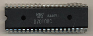
NEC uPD70108C – V20 CPU – Late 1984

NEC had a cross license agreement with Intel dating back to April of 1976 that allowed each company to make/sell products based on each others patents.  This was particularly important in the 1970’s as having a viable ‘second source’ for your designs was considered critical for it to be viable in the market.  This was especially true for Intel, who wanted to get into the Japanese market. In 1979 NEC began to produce and sell the 8086 and 8088 processors.  NEC wasn’t going to succeed by just being a second source to Intel though, designing their own processors was of great importance.  While producing the 8086/8088 they also began working on their own version, which would be an enhanced 8086/8088 processor.

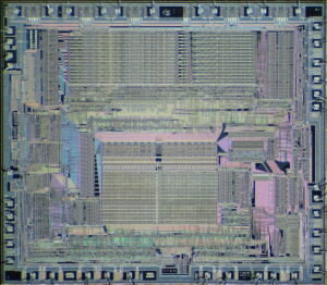
NEC V30 Die (courtesy Birdman) – 8086 with many enhancements

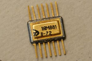
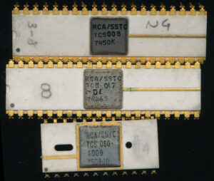
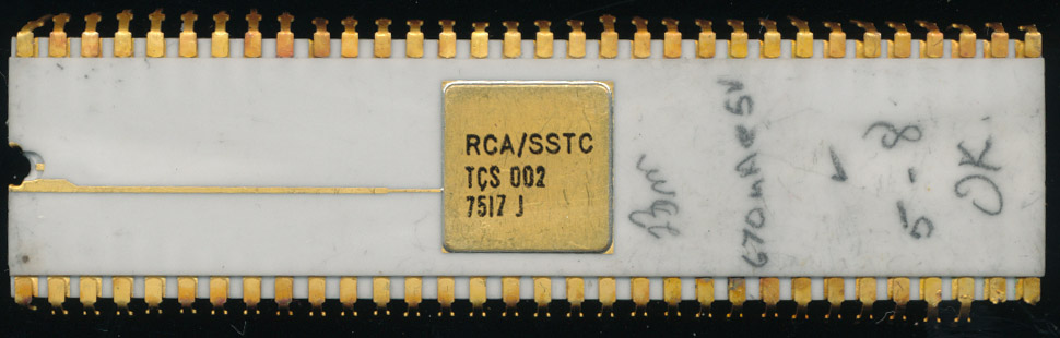
The result was the rather well known V20/V30 processors of 1984.  These were not just clones of the Intel MCS-86 (though determining this took several court cases and resulted in the Chip Act of 1984).  The V30 had some pretty big differences, notably, internally it had dual 16-bit busses, allowed data to be moved much more efficiently, as data could be moved into and out of a register at the same time (nearly).  It also increased the microinstruction word from 21 bits to 29 bits, added a hardware effective address generator, additional instruction pointers, and a hardware shift/loop counter.  Taking advantage of these features added some new instructions as well, 156 compared to the 8086’s base 133.  The V30/V20 were the beginning of a line of V-series processors.  NEC went on to make  ‘186/188 style processor (the V40/V50) as well as a series of microcontroller versions  (V25/V35 and others).  The V20/V30 were to be supported by a math coprocessor like the 8087 called the upd72091.  Very little info is available on the 72091 as it was cancelled very early on in its design, as by 1984-1985 it was already out of date.  Its replacement was to be a bit more powerful.

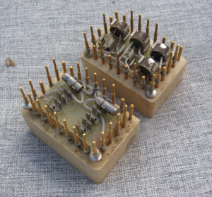
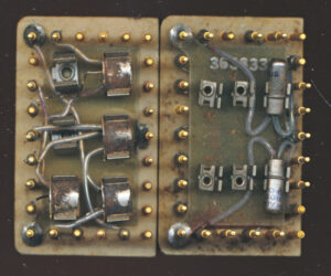
Design of the the upd72191 started likely at the same time the V30 was released, around 1984-85, with specifications released in 1986, and plans for chips by 1987.  This chip was in an advanced state of planning, such that many products, including motherboards (such as the Ampro Little Board PC) and industrial controllers designed with sockets for it.  Preliminary datasheets exist, but alas, no chips seem to be found.

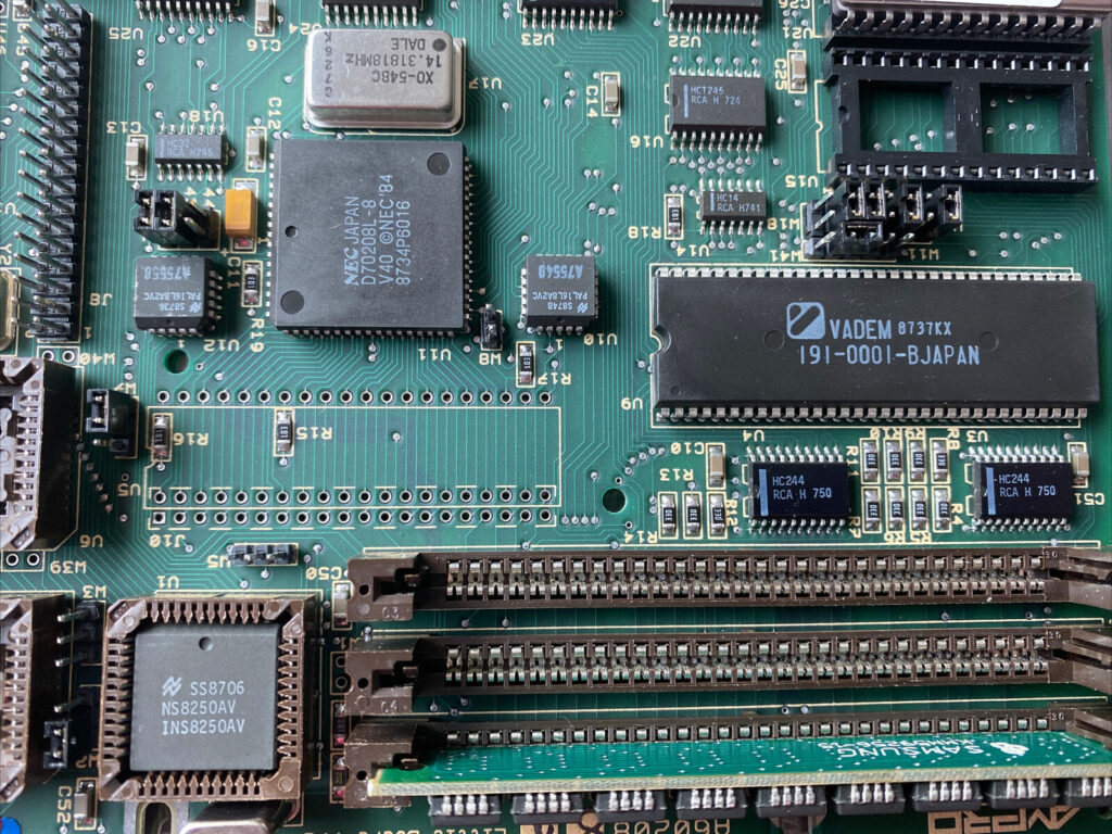
LittleBoard PC (Ampro) with support for canceled upD72191 (V40 based)

The upd72191 was made in CMOS and is a bit like an enhanced 80C187 but with support for the V20/V30.  It is fully IEEE-754 compatible (the 8087 wasn’t as the standard wasn’t finished yet) and supports a similar instruction set as the 80C187 (and thus the 80387).  Unlike the 8087 it supports the full set of Exponential, Trig, Logarithmic, and Hyperbolic instructions.  The 8087 was somewhat limited in this, as it was already pushing the limits of what was possible on a single chip at thee time of its release.  The 72191 supports FSIN/FCOS which the 8087 doesn’t and many other functions (its full instruction set could not be found).  The 72191 has a mode pin that selects between interfacing between the V20/V30 and the V40/V50, (as these talked to coprocessors differently) so it was compatible with 4 distinct processors.  The 80C187 could only be used with the 80186 and the 8087 could only be used with the 8086/8088.

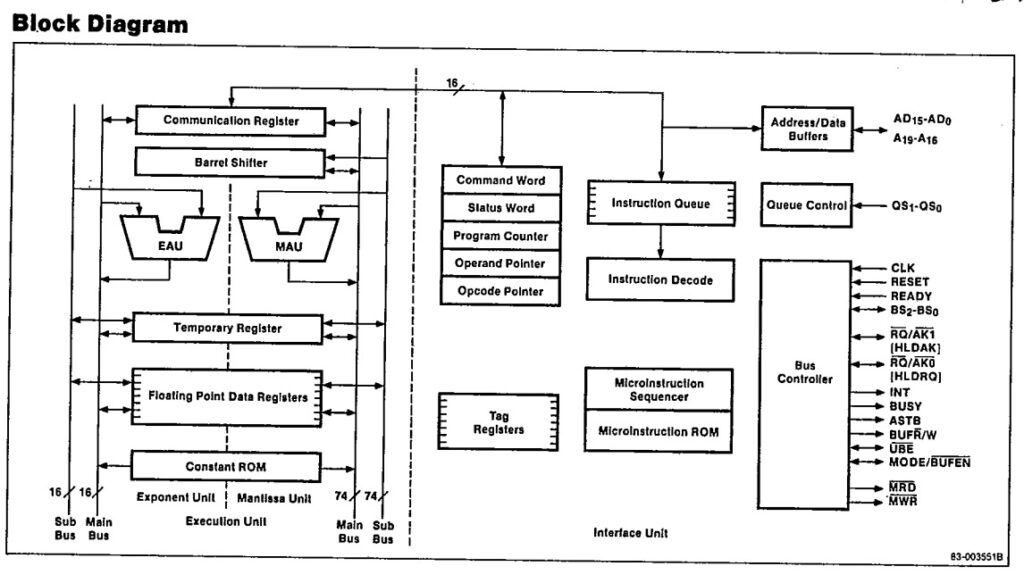
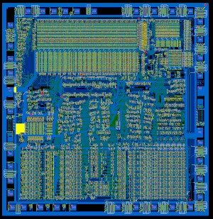
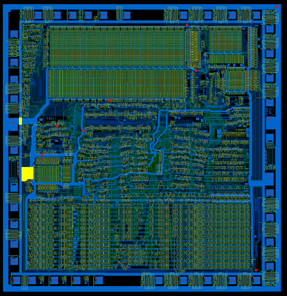
upD72191 FPU Block Diagram – 1986ish

Looking at the block diagram of the ‘191 we notice something else, its a dual bus design, much like the V30 processor.  Internally there are a pair of 74-bit busses for the mantissa (fraction) side and a pair of 16-bit busses for the exponent side.  This is a striking difference from that of the 8087 and the ‘187.  The 8087 has a single 16-bit bus for the exponent, and a 64-bit (68-bits into the shifter and ALU) for the mantissa.  There are 3 extra bits for enhanced accuracy, and a extra leading bit that is always 1 for floating point math, giving 64 bits of ‘data’.

The dual bus design makes sense as NEC did the same for the V-series.  Coupled with the right microcode, it can greatly enhance the speed of the FPU.   So why then is the bus expanded to 74-bits for the mantissa?   In the 80187 and 80387 this bus is still only 68-bits.  We look to the design of NECs follow on FPU for the answer.  The upd72291 (and its 32-bit bus 72691 version) are rather different beasts, made for the the V33/V53 x86 CPUs and V60/V70/V80 non x86-CPUs.  We’ll talk about them in more detail later, but they share the same 74-bit mantissa as the 72191, and in this case, the designers wrote a paper on its design.

The FPP [72691] is the only floating point processor that provides the power function xy.  This function (called FPOWER in the instruction set) is difficult to implement not only for its complex definition but also for sufficient accuracy. The equation Xy = e(y*logeX)
does not give good accuracy because the accuracy error of the log function is augmented by the exponential function.  The FPP solves this problem by providing a 74-bit data width for the mantissa data bus.

Being as the 72191 was canceled, the ‘291/691 would in fact have been the only FPU to support this in hardware, but it seems it was first implemented on the ‘191.  The solution only works well for larger (greater then 32) values of y, otherwise iterative multiplication is used, but where it can be used it greatly speeds up the calculation.

When the 72191 was canceled NEC thoughtfully provided a single chip solution called the upd9335C for allowing an 8087 to be interfaced to the V40/V50 processors which, like a 186, used a HOLD/HOLDACK bus release protocol instead of the 8086/8088s (and V20/V30s) REQUEST/GRANT.  For applications using a V20/V30, an 8087 could be used directly.

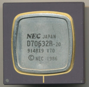
NEC upD70632R-20 20MHz V70 Processor

In 1989 NEC released the next of the V-series, the V60, V70 and later the V80 processors.  These were a departure from the previous in that they were no longer based on the x86 architecture, but rather a completely new ISA (though the V60 and V70 had a V20/V30 emulation mode).  These were full 32-bit designs, and were Japan’s first widely available 32-bit processors.  Of course with a new processor comes the need for a new FPU and NEC had not one, but 2 FPU options for these.  The upd72291 and upd72691 are based on the same design, but with some major feature differences.  The 72291 is designed to work with processors that have a 16-bit data bus such as the V60.  It also could be used with the older V33/V53 x86 designs.  Internally it has eight floating point registers and supports all your typical floating point functions as well as vector math functions.  The upd72691 is designed for 32-bit data paths, but adds a bit more…

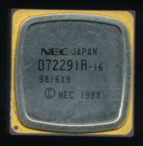
NEC updD72291R-16 FPU

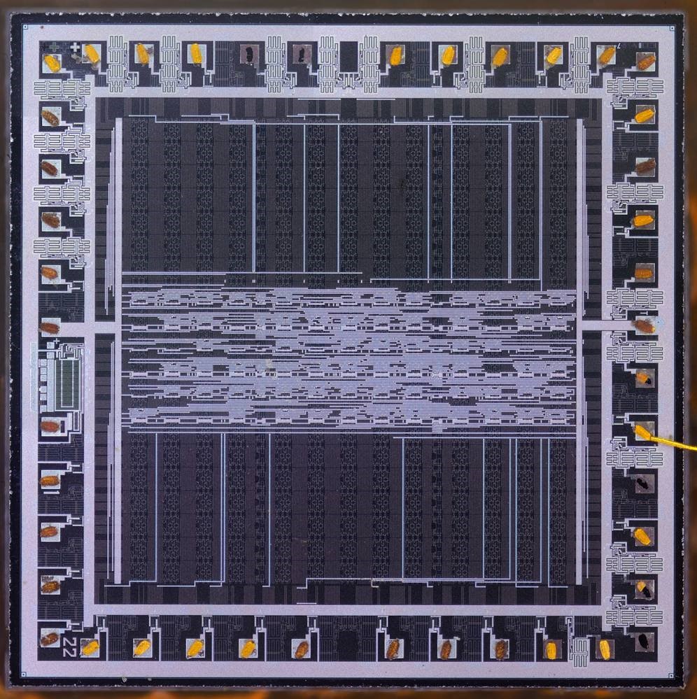
In addition to expanding the register set to 32 FP registers, the ‘691 also added a complete suite of matrix  math functions. The ‘691 was made on a 1.2u CMOS process and contained 433,000 transistors. (nearly 50,000 MORE then the V60 processor) Running at 20MHz it was capable of around 6.7MFLOP and supported 24 vector/matric instructions as well as 22 mathematical functions.  Like the 72191 it had a 74-bit mantissa datapath, but expanded the exponent path to 17-bits to support double extended precision number formats. It is a highly microcoded design using a 3072 word (43 bit word) microcode ROM, 20% for vector/matrix, 37% for arithmetic, and the rest for exceptions handling and other house keeping instructions. Interestingly, these microps themselves encode additional instructions that NEC call nano-ops, these controlled just the ALU operations of the instruction (the rest being bus control and sequencing).  These nano-ops were stored in a 256 word x 74-bit Nano ROM (only 120 words were used, the rest for potential expansion). This was the last of the line of NECs dedicated FPUs (excluding the few MIPS FPUs they made).  Its a bit ironic that it seems they canceled as many designs as they made.

…but perhaps they didn’t?

Read More »

Tags:
, , , , ,

Posted in:
CPU of the Day

August 12th, 2021 ~ by admin

Forgotten Italian CPU – The Genesys B52 MMX

Introduction

On this site you can read about thousands of processors models. And every year it is more and more difficult to write about some new (old) processors, since everything has been known for a long time. But there are also exceptions to the rule which we love to find. In 2021, I learned about one unusual processor, the information about which I want to share with you. The roots of this processor’s history go back to Italy, in the distant year or 1998. This time just falls on the confrontation between Intel and its second generation Pentium and AMD K6-2 and K6-3 processors. The Cyrix MII processors from Cyrix Corporation, IDT WinChip 2s and Rise mP6s were still going strong as well.

But before we talk about the Genesys B52 MMX processor, we should take a closer look at Intel Pentium II processors in general, as the Italian processor primarily owes its appearance to them.

Intel Pentium II

From 1993 to 1997, the Pentium dominated all market segments. Over time, the name of the “Pentium” trademark even grew into a household name (Its all about the Pentiums baby), but with the release of the Pentium II, everything changed. If earlier Intel did not deeply segment the market, there were Pentium Pros for workstations and servers, and for everything else there were various models of Intel Pentium processors, in which, at the end of their domination, Intel added MMX instructions, depriving and thereby putting an end to its server segment. The new slot form factor of the processor, the abandonment of the usual pins and ceramics and further segmentation of the market (using Intel Celeron processors and the new Xeon line) radically changed the further course of development of the history of microprocessors.

May 7, 1997 saw the light of the first models of Intel Pentium II processors, manufactured on a 350nm process with a core voltage of 2.8 volts. The first models were based on the Klamath core (named after the river by which The CPU Shack is located) core, operating at 233 and 266 MHz. The main differences from the Pentium Pro predecessor it was based on were the L1 cache increased from 16 to 32 Kb, and the presence of a block of SIMD instructions called MMX first introduced on the last P55C processors. Like the Pentium Pro it featured its own L2 cache on the module, but in this case it was 512KB fixed on the same PCB as the processor core, a much cheaper solution then the dual ceramic cavity package of the Pentium Pro.

Before the Pentium II, only the Pentium Pro could boast of its own cache, running at the frequency of the CPU core. But, placing the CPU core and L2 cache on the same substrate was an expensive pleasure even for Intel, and the processors had to be cheaper for better competition, which was getting more and more intense. Intel then made a “wise” decision, as a result of which the Pentium II got a its own L2 cache next to the CPU core This engineering solution significantly reduced the cost of manufacturing processors. BSRAM L2 cache chips were manufactured by Toshiba, SEC and NEC at that time, rather then being made in house by Intel, further easing the cost burdens.

Pentium II Klamath SECC1 PBGA Core 2 x Cache on front 2x + TAG on back

For all models of Pentium II processors, the cache size remained unchanged and equaled 512 KB, while different Pentium Pro models had a cache from 256 to 1024 KB. The L2 cache of the first Pentium II processors consisted of four microcircuits located on both sides of the cartridge processor board and operated at half the core frequency. In addition to the processor core and 4 L2 cache chips, there was also a tag-RAM chip on the cartridge PCB, a total of 6 IC’s.

Backside with 2x cache + TAG

The tag-RAM size/configuration determines which range of main memory can be cached. For example, if the L2 cache is 256 KB and the tag RAM is 8 bits wide, then this is enough to cache up to 64 MB of main RAM. However, if you add additional RAM in the process, it will not be cached unless you also expand the tag RAM. On Socket 1-3 486 systems, most motherboards allowed adding and modifying additional L2 cache and tag-RAM chips for this purpose. The Pentium Pro had built-in L2 cache and tags capable of caching up to 4GB of main memory, whereas the first Pentium IIs could cache up to 512MB of RAM.  This was in part to set them apart from the server oriented Pentium II Xeon which had full speed cache capable of caching 4GB (or 64GB with PSE-36),

In January 1998, Intel announced the Pentium II processor, built on a new core, codenamed Deschutes (Another river in Oregon). The processor core was manufactured using the smaller 250nm process, which lowered the operating voltage to 2.0 V, instead of 2.8 V for “Klamath”. The L2 cache of 512 KB still worked at half the core frequency, but it was made in the form of two BSRAM chips located to the side of the processor package. In later modifications of the Pentium II Deschutes core, Intel replaced the tag-RAM chip, thanks to which the processors could cache up to 4 GB of RAM (the 82459AD revision).

The first generation of Intel Celeron processors were based on the “Covington” core were essentially processors on the “Deschutes” core, but without ANY L2 cache. Thanks to this, they had very poor performance, but they overclocked very well, demonstrating the best overclocking figures up to double the nominal clock frequency.

Deschutes core with Organic BGA core and 2x cache chips on front. TAG on back

All overclocking of Pentium II, as a rule, rested on the characteristics of microcircuits used by BSRAM and tag-RAMs. The latter, like the cache, was much disliked voltage rises, and with inept handling, an expensive Pentium II could turn out to be a Celeron “Covington”, if such microcircuits failed.By the way, they warmed up decently on Pentium II processors based on the “Klamath” core so cooling was very important as well. The multiplier in 99% of Pentium II processors was locked (very early production ones were unlocked and Engineering Samples of course), so overclocking was performed by raising the FSB frequency, this being dependent always on the cache and TAG chips installed in that particular processor.


A simple example. In Costa Rica, where Intel has an advanced advanced processor assembly/test factory, which simultaneously assembled high-frequency models with 450 and 300 megahertz. The cartridge and core for these processors are identical (and the multiplier was the same 4.5x as well 66×4.5 for the 300 and 100×4.5 for the 450). The difference was only in the installed cache memory with different speed rating in nanoseconds. Sometimes on the assembly line there was only a fast cache memory capable of operating at a frequency of 225 MHz, intended for models of processors with 450 MHz. In this case, it was also installed on the model with a frequency of 300 MHz, as a result of which they overclocked perfectly.

Genesys B52 MMX CPU

The history of the Italian processor began in the city of Monopoli, in the province of Bari in Italy. In 1998, Italian Marcello Console founded Genesys, which initially employed 10 people. The main idea of the Genesys business was the production of modified Intel Pentium II processors based on the “Deschutes” core, at a much lower price than the Pentium II ones of similar clock speed. Plus a warranty period extended to 3 years and productivity increased by 5% or more. It turns out to be a solid Attraction of Generosity!

Genesys had registered its own domain www.b52mmx.com and is getting ready to implement their processors in ready-made system units. Unfortunately, nothing is known about the manufacturing process, it remains a mystery to this day. There is not so much information on these processors, but let’s try to figure out what these processors were.

Read More »

August 2nd, 2021 ~ by admin

The 6502 Travels the World: The Story of the Indian SCL6502

Semiconductor Complex LTD SCL6502 CPU

India in the 1970’s was often considered a third world county, supported by a largely agrarian economy and with a wide swath of the population still based off of subsistence living.  They also however, had a robust space program, had mastered nuclear technology and had a largely stable government that supported the advancement of technology development in the country.  All the pieces were there to begin making the shift to the robust high tech economy that they possess today.  In the 1970’s India had several govt entities working on semiconductors and electronics, all managed under the direction of the Dept of Electronics.  There was also a fair number of companies with plants in India doing electronics manufacturer and assembly.  This was largely small scale production of older technology.  TTL circuits  (starting with the 7420) were made in Bangalore by BEL back in 1971.  But TTL circuits won’t get you far, and at that time the best process India had was around 8 microns, so in 1972 an initiative was started to develop an indigenous semiconductor industry within India.

SCL Fab – Currently 0.18 Micron

Politics are the same everywhere, and so this process took some time, people with experience had to be recruited to run it, and a suitable (politically and geographically) location selected.  Eventually in the late 1970’s the Semiconductor Complex LTD was formed in the city of Mohali ( Chandigarh ) in the Punjab province of India.  SCL was to be the state supported enterprise to bring indigenous high end (LSI and above) semiconductor production to India.  Two things were needed to make this work: Technology, and People who were experts in that field.  SCL was tasked with going to Japan, America, and Western Europe in search of a company that would assist with the technology transfer, as well as finding some Non-Resident Indians who would be willing to come back to India to work on it.  Many Indians had high skill jobs in the industry outside of India, and it turned out convincing them to come back to help their country was a non-issue (though generous incentives were provided).  Getting the technology on the other hand was a bit more work.

The first trip of the technology transfer team of SCL was to Hitachi in Japan.  Negotiations with Hitachi were grueling, and while not unproductive, did not yield the results SCL wanted.  Hitachi was happy to license some designs to SCL, for a high fee and royalties, but did not want to immediately help create the 3-5 micron production fab that SCL envisioned.  Hitachi called thei ‘one step at a time’  whereas the Indians wanted to go all in from the start.  Hitachi agreed only to help (some) with a 5 micon process) and only to license products for digital clocks and watches.  The SCL team then turned to the United States, likely expecting similar results.

The chosen company in the USA was AMI (American Microsystems Inc), a company with 7-8 times the turnover of Hitachi.  AMI was at the time the largest maker of custom ICs in America, as well as a very large provider of second source ICs  (such as the 6800 and 9900 CPUs).  AMI’s CEO Roy Turner readily agreed to help SCL, much to the surprise of their negotiation team, and on the very first day offered SCL AMI’s 5 micro CMOS and NMOS processes, with the option to license their 3 micron CMOS and NMOS processes within 4 years of the agreement becoming effective.  AMI also offered SCL access to all of AMI’s standard products catalog, as well as the possibility of joint development of additional products, all at a simple 50/50 split.  AMI even offered to help with the technology export license that would be required by the US State Dept to transfer the fab tech to India.  The agreement was signed in April of 1981.

Read More »

Tags:
,

Posted in:
CPU of the Day

July 15th, 2021 ~ by admin

The Intel 8086 Gets ICE’d

A while back I received this rather unusual board. Made in 1979 it was clearly a prototype, being a completely handmade wire wrapped board made ona standard Intel MULTIBUS breadboard from 1974. No CPU was present, but a 3M TEXTOOL socket for a CPU is. The paper sticker on the board reads ICE-86/86A/88/88A TEST FIXTURE K95 and DSO TEST ENGINEERING.

ICE-86/86A/88/88A Prototype Test Board

The ICE-86 (and ICE-86A/ICE-88/88A) were all MULTIBUS In circuit Emulators Intel made for the iAPX86 processors in 1979-1985 or so. These were 3 board sets, with a emulator pod (containing a 808x processor) meant for developing and testing x86 software and hardware designs. The boards would plug into a Intel MDS or MDS2 system (or Intel Intellec) and with supporting software, formed the basic of much of the original x86 hardware/software design of the era.  I assumed this board was part of that set, but alas, while researching it I got ICE’d.

Remember wire wrapping? And using all one color for everything?

The ICE-8x systems are based on a Intel 8080A processor, so I checked the pinout on the socket on the prototype, VCC/GND did not match that of an 8080A CPU, it DID match that of a 8086.  Furthermore the clock generator on the board is a P8284, thats the clock generator for the 8086/88 processor, taking the 15MHz crystal input, and outputting a 5MHz clock. The 8080A processor of the ICE-86 emulator system uses a 8224 clock generator (which is a divide by 9 clock generator, usually running on a 9-10MHz or 18-19MHz Crystal).  To make matters more interesting I also have a couple later board (1982 production) which are clearly production (likely limited as the part numbers are still hand written) of the prototype.  They are labeled as ICE-86 TEST – 1981.

Production version of the ICE-86 TEST made in early 1982. Curiously this is a MULTIBUS board but about an inch (2.5cm) taller than standard. This was probably not meant to remain in a host system for long.

The prototype has a switch on it labeled ‘ICE’ for switching the board from 8086 mode to 8088 mode, while the production board lacks such a switch (its designed solely for 8086 processors).   The prototype has a pair of D3604A 4k (512×8) PROMs, the production version is running a pair of 3628A 8k versions,m which were not available when the prototype was made.  So what then would the purpose of such a board labeled ICE, that well, isn’t an ICE?

These board’s were designed for testing ICE emulators, and eventually giving end users the ability to test their software on a known working 8086/88 system.  Generally when using an emulator, you would plug the probe into the processor socket on the target system you are developing and the emulator system allows you to set breakpoints, check register values, memory, etc.  These test boards would allow you to develop at least basic software WITHOUT having a target system of your own, as well as to be able to offer an in system test of the entire ICE emulation.  The production boards being labeled ‘ICE 86 TEST’ seem to be just this, how to ensure the proper function of the by then, thousands of ICE-86/88 board sets now in use.  There was very likely a separate board for testing the ICE-88/A systems as well.  Plug the tester into a MULTIBUS slot on the host system, plug the probe cable into the ZIF socket, and run the testing software.  The ROM’s on the proto board are labeled ‘STIPOL’ which is cryptic at best, but onc of their purposes would likely to be to provide STImulus of somesort to the ICE emulator being tested.

The test boards would also give developers either peace of mind or headaches, when designing for the x86, is the problem the emulator not working? or is their a bug in my design?  Now I need to find boards from an actual ICE-86 system.

Tags:
, ,

Posted in:
Boards and Systems

June 27th, 2021 ~ by admin

Navy Hydrophone Noise Canceller: Weitek 3332 Floating Point Based DSP

Navy 55910 ASSY 0120811 Eight Channel DSP – Serial #1

I got these boards some time ago, hoping to be able to figure out more about them but alas, information is very sparse, but they are such good looing boards, with impressive technology for the day, I had to post them

These boards came out of a US Navy system labeled “Hydrophone Noise Canceller”  which seemed to be part of SONAR test system at a University.  These date from the late 1980’s to the early 1990’s. The system was comprised of 16 boards, 12 8 Channel DSP board, a control board, and 3 Ethernet Boards,  Each of these boards is a very heavy 4 layer PCB, with pretty much everything socketed.

The DSP Boards are based on the Weitek 3332 FPU. These are full 32-bit Floating point datapaths (MULT/DIV/ADD/SUB + Registers) and made on a CMOS process.  They operate on a 100ns (10MHz) clock.  THese are the higher end version of the 3132, they have a full 3 busses versus the single bus of the 3132.  These 3 busses add a lot to the pincount (168 vs 144) and thus cost but make designing a system more flexible, no bus sharing to worry about.  The 3332 was designed specifically to support high speed DSP and graphics processing.  It performed the ‘core’ of a DSP, allowing the user to build around it and make essentially a custom DSP for their application (unlike the purpose built TI TMS320 series of DSPs also available at them time) On the board they are backed by 4 Cypress CY7C128 2K SRAM per processor (8K total).  There is no clock crystal on the board itself, which is typical of a system like this.  To ensure everything stays in synch, the clock would be provided by the control board and distributed to each of the boards on the bus.

Navy 55910 ASSY 0125321 Controller A80386DX-25 (20MHz) Serial #2

The Control Board runs an Intel A80386DX processor.  On this particular board its a 25MHz chip, but note the crystal next to it is an 80MHz crystal.  A 386 internally divides the clock by 2, so the 80MHz clock is most like divided by 2 externally resulting in a 40MHz input to the 80386, and a 20MHz CPU clock.  I had another controller board with a 20MHz 80386 so they probably just used what ever they had available.  This is Serial # 2 afterall.  The 386 is supported by 4 27C256 EPROMs and 8 32K (CY7C198) SRAM chips, giving it 256K of SRAM.  In addition is 12 8k (CY7C185) 8K SRAM chips each with there own Pipeline Register.

A typical 386 system would have several MB of RAM, but this system is set up for real time data processing, as a DSP system, so the only data that needs to be in RAM is the control program itself, so 256K of system RAM is a great plenty.  Additional RAM is likely used solely for buffering data from the Hydrophones.

It would be interesting to know what this board was used for in more detail, but even if that never happens its an interesting board for its time.  Clearly a vast amount of effort went into designing and building the system.


Tags:
,

Posted in:
Boards and Systems

June 19th, 2021 ~ by admin

Intel P54CM Pentium: The Dual Pentium Processor

Intel Pentium P54CM – Q0475 Engineering Sample from November 1993

Today dual processors are incredibly common, even in home computing, and multicore processors even more common, but there was a time when this was not so.  There were of course multi-processor systems in the 80’s and early 90’s, but these required extensive additional hardware to support them.   Three main concerns for design multiprocessing systems are how to efficiently handle interrupts (which CPU handles what), how to ensure the caches are kept current (and not used if they aren’t), and how do processors share the same bus.

Bus sharing was largely handled already as busses have long been shared by all sorts of devices.  Interrupts were made easier by the release of the APIC (Advanced Programmable Interrupt Controller) standard by Intel in the early 1990’s.. The first version of this was implementing in the 82489DX IC.  Each CPU (486 or original P60/66) would need its own 82489DX (Local APIC) and then yet another one to work as an I/O APIC.  Clunky, but it worked.  The BIOS and OS were designed to help with cache coherency coupled with the a modified MESI protocols in the processors themselves for keeping track of what cache items were valid or not.

P54CM50-75 Q033 – Early October 1993 Sample – 75MHz modified Socket 5

After the release of the first (P5 Socket 4) Pentiums Intel decided to integrate  an APIC onto the CPU core itself.  This greatly simplified dual processor setups.  Within only a few months of the release of Socket 4, Intel was already working on the P54C Pentium.  These were to be on a whole new socket, Socket 5 (much to the annoyance to those who had just dropped some serious coin on a Socket 4 system).  The Socket 5 systems, using the Intel Neptune 430NX chipset, would support dual processor systems.  To do this Intel designed a separate Pentium Processor core called the P54CM, and originally, a separate, slightly modified socket for it.  The secondary socket had a slightly different pin out, and was to run the P54CM processor, OR, could be used as an OverDrive socket, with the Overdrive becoming a second CPU (why both, no one is entirely sure).

P54CM50-75 Q033 – Mod Socket 5 – Oct 1993 Q0475 Nov 1993 – Standard Socket 5

Samples of the P54CM debuted in October of 1993 using the new pinout.  Samples from just weeks later had reverted to the standard Socket 5 pinout, clearly someone at Intel decided that yet another socket (and package) design would be uneconomical.  The separate core, however, remained.

Early Pentium Print Ad shows the modified Socket.

The P54CM core was only produced in a very few specs, SX874 B1 stepping in STD Voltage (3.135V–3.465V) and the SX942 (STD) SX943 (VRE 3.3V–3.465V)  and SX944 (MD: faster timings on several pins/3.135V–3.465V) series in the B3 stepping.  There were also several ES versions made: Q033 P54CM50-75, Q0475, Q0519 and Q0520 with the B0 stepping and Q0543 with the B1 stepping.  These processors, including the production versions, were incredibly rare.  Very few companies used them in actual machines.  Why? Because a normal (providing it supported dual processing) P55C could be ran just as well.  The only real difference in the P54CM core was the DPEN/ output pin was driven low on RESET.  On a P54CM this pin is an output that tells the primary processor ‘hey a second processor exists’ while on the standard P54C, DPEN/ is an input.

SX874 – P54CM-B1 (with the FDIV bug) from October 1994

It turns out that the P54C/CM core ALSO has a CPUTYPE pin that can be be set to tell a system that the processor is a secondary processor or a primary (and early Pentium Dual boards had a jumper to do just this.)  You didn’t actually NEED a P54CM as the secondary processor. a normal P54C would work just fine.  There was even some trickery to allow a system to boot off of a secondary P54CM CPU, not officially supported by Intel, but in systems designed for redundancy, the DPEN/ pin could be overridden and the P54CM used to boot a system (normally the primary CPU would handle all the boot up duties and only enable the secondary CPU once it was ready).

Later Socket 5/7 Pentiums (C0 and later steppings) supported multiprocessing natively with a few exceptions.  The SU114/SL25H Pentium 200s did not have a functional APIC so thus were not DP compatible.  These were even mismarked by Intel, with the marking ‘VSS’ on the back.  That last ‘S’ means they were tested to support UP, DP and MP configurations, when in fact they were not, the code on the back should have been VSU (‘U’ means they were tested for MP, and uniprocessor, but NOT DP, as DP required a working APIC).  The SY045 (200) and SY037 (166) were also ‘VSU’ processors, not tested for DP use, likely because of some issue with the APIC.

Mismarked SU114 (VSS) and correctly marked SY045 VSU

Intel Overdrive processors suffer a similar fate, they will not run in the primary socket of a DP system, but will in the secondary socket.  This is mostly likely because the DPEN/ is not supported as an input on the Overdrive, so it wouldn’t know a secondary processor exists, a shame really as a dual OverDrive system would be pretty neat.

At he beginning of the P5 era Intel seemed to be all in on DP systems, but with the coming release of the Pentium Pro, they began to use Dual Processing as a way to differentiate their products.  DP support was removed in the next Pentium chipset (the FX Triton) only to later return in the HX Triton II.  The VX and TX Pentium Chipsets also lacked DP support.

Quite famously later in the 1990s Intel marketed the Pentium II/III with multi-processor support, and sold the Celeron as uniprocessor only.  It turned out that the lowly Celeron was quite happy to run in DP configuration, much to the annoyance of Intel, but joy of enthusiasts around the world.  Perhaps someone will figure out a way to run Pentium Overdrives in dual processor systems, if there is a will there tends to eventually be a way.


Posted in:
CPU of the Day