
NEC’s Forgotten FPUs
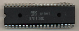
NEC uPD70108C – V20 CPU – Late 1984
NEC had a cross license agreement with Intel dating back to April of 1976 that allowed each company to make/sell products based on each others patents. This was particularly important in the 1970’s as having a viable ‘second source’ for your designs was considered critical for it to be viable in the market. This was especially true for Intel, who wanted to get into the Japanese market. In 1979 NEC began to produce and sell the 8086 and 8088 processors. NEC wasn’t going to succeed by just being a second source to Intel though, designing their own processors was of great importance. While producing the 8086/8088 they also began working on their own version, which would be an enhanced 8086/8088 processor.
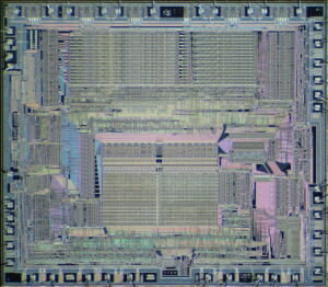
NEC V30 Die (courtesy Birdman) – 8086 with many enhancements
The result was the rather well known V20/V30 processors of 1984. These were not just clones of the Intel MCS-86 (though determining this took several court cases and resulted in the Chip Act of 1984). The V30 had some pretty big differences, notably, internally it had dual 16-bit busses, allowed data to be moved much more efficiently, as data could be moved into and out of a register at the same time (nearly). It also increased the microinstruction word from 21 bits to 29 bits, added a hardware effective address generator, additional instruction pointers, and a hardware shift/loop counter. Taking advantage of these features added some new instructions as well, 156 compared to the 8086’s base 133. The V30/V20 were the beginning of a line of V-series processors. NEC went on to make ‘186/188 style processor (the V40/V50) as well as a series of microcontroller versions (V25/V35 and others). The V20/V30 were to be supported by a math coprocessor like the 8087 called the upd72091. Very little info is available on the 72091 as it was cancelled very early on in its design, as by 1984-1985 it was already out of date. Its replacement was to be a bit more powerful.
Design of the the upd72191 started likely at the same time the V30 was released, around 1984-85, with specifications released in 1986, and plans for chips by 1987. This chip was in an advanced state of planning, such that many products, including motherboards (such as the Ampro Little Board PC) and industrial controllers designed with sockets for it. Preliminary datasheets exist, but alas, no chips seem to be found.
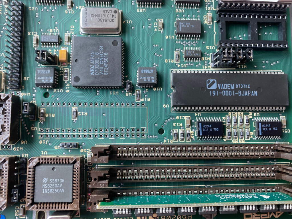
LittleBoard PC (Ampro) with support for canceled upD72191 (V40 based)
The upd72191 was made in CMOS and is a bit like an enhanced 80C187 but with support for the V20/V30. It is fully IEEE-754 compatible (the 8087 wasn’t as the standard wasn’t finished yet) and supports a similar instruction set as the 80C187 (and thus the 80387). Unlike the 8087 it supports the full set of Exponential, Trig, Logarithmic, and Hyperbolic instructions. The 8087 was somewhat limited in this, as it was already pushing the limits of what was possible on a single chip at thee time of its release. The 72191 supports FSIN/FCOS which the 8087 doesn’t and many other functions (its full instruction set could not be found). The 72191 has a mode pin that selects between interfacing between the V20/V30 and the V40/V50, (as these talked to coprocessors differently) so it was compatible with 4 distinct processors. The 80C187 could only be used with the 80186 and the 8087 could only be used with the 8086/8088.
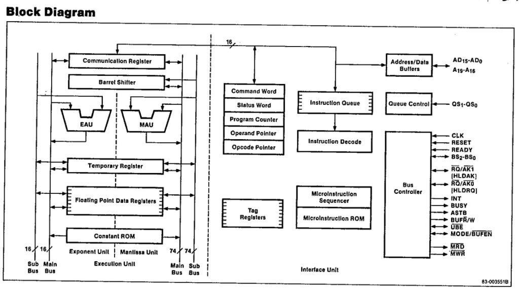
upD72191 FPU Block Diagram – 1986ish
Looking at the block diagram of the ‘191 we notice something else, its a dual bus design, much like the V30 processor. Internally there are a pair of 74-bit busses for the mantissa (fraction) side and a pair of 16-bit busses for the exponent side. This is a striking difference from that of the 8087 and the ‘187. The 8087 has a single 16-bit bus for the exponent, and a 64-bit (68-bits into the shifter and ALU) for the mantissa. There are 3 extra bits for enhanced accuracy, and a extra leading bit that is always 1 for floating point math, giving 64 bits of ‘data’.
The dual bus design makes sense as NEC did the same for the V-series. Coupled with the right microcode, it can greatly enhance the speed of the FPU. So why then is the bus expanded to 74-bits for the mantissa? In the 80187 and 80387 this bus is still only 68-bits. We look to the design of NECs follow on FPU for the answer. The upd72291 (and its 32-bit bus 72691 version) are rather different beasts, made for the the V33/V53 x86 CPUs and V60/V70/V80 non x86-CPUs. We’ll talk about them in more detail later, but they share the same 74-bit mantissa as the 72191, and in this case, the designers wrote a paper on its design.
The FPP [72691] is the only floating point processor that provides the power function xy. This function (called FPOWER in the instruction set) is difficult to implement not only for its complex definition but also for sufficient accuracy. The equation Xy = e(y*logeX)
does not give good accuracy because the accuracy error of the log function is augmented by the exponential function. The FPP solves this problem by providing a 74-bit data width for the mantissa data bus.
Being as the 72191 was canceled, the ‘291/691 would in fact have been the only FPU to support this in hardware, but it seems it was first implemented on the ‘191. The solution only works well for larger (greater then 32) values of y, otherwise iterative multiplication is used, but where it can be used it greatly speeds up the calculation.
When the 72191 was canceled NEC thoughtfully provided a single chip solution called the upd9335C for allowing an 8087 to be interfaced to the V40/V50 processors which, like a 186, used a HOLD/HOLDACK bus release protocol instead of the 8086/8088s (and V20/V30s) REQUEST/GRANT. For applications using a V20/V30, an 8087 could be used directly.
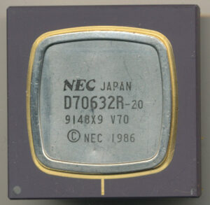
NEC upD70632R-20 20MHz V70 Processor
In 1989 NEC released the next of the V-series, the V60, V70 and later the V80 processors. These were a departure from the previous in that they were no longer based on the x86 architecture, but rather a completely new ISA (though the V60 and V70 had a V20/V30 emulation mode). These were full 32-bit designs, and were Japan’s first widely available 32-bit processors. Of course with a new processor comes the need for a new FPU and NEC had not one, but 2 FPU options for these. The upd72291 and upd72691 are based on the same design, but with some major feature differences. The 72291 is designed to work with processors that have a 16-bit data bus such as the V60. It also could be used with the older V33/V53 x86 designs. Internally it has eight floating point registers and supports all your typical floating point functions as well as vector math functions. The upd72691 is designed for 32-bit data paths, but adds a bit more…
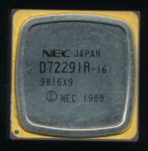
NEC updD72291R-16 FPU
In addition to expanding the register set to 32 FP registers, the ‘691 also added a complete suite of matrix math functions. The ‘691 was made on a 1.2u CMOS process and contained 433,000 transistors. (nearly 50,000 MORE then the V60 processor) Running at 20MHz it was capable of around 6.7MFLOP and supported 24 vector/matric instructions as well as 22 mathematical functions. Like the 72191 it had a 74-bit mantissa datapath, but expanded the exponent path to 17-bits to support double extended precision number formats. It is a highly microcoded design using a 3072 word (43 bit word) microcode ROM, 20% for vector/matrix, 37% for arithmetic, and the rest for exceptions handling and other house keeping instructions. Interestingly, these microps themselves encode additional instructions that NEC call nano-ops, these controlled just the ALU operations of the instruction (the rest being bus control and sequencing). These nano-ops were stored in a 256 word x 74-bit Nano ROM (only 120 words were used, the rest for potential expansion). This was the last of the line of NECs dedicated FPUs (excluding the few MIPS FPUs they made). Its a bit ironic that it seems they canceled as many designs as they made.
…but perhaps they didn’t?
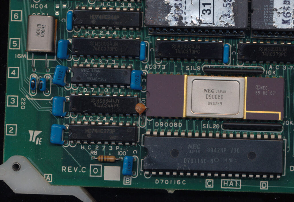
Board with NEC V30 and the mystery NEC D9008D chip. Ran off a 16MHz clock (through a D71011C clock generator)
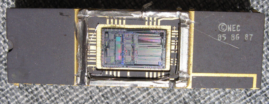
The story of NEC’s FPUs is interesting, but as is usually the case, something led me down this path. While looking through loads of old scrap boards I found a most curious arrangement, a board with a normal unassuming V30 processor, but right next to it was another 40-pin chip, a chip with a HUGE die lid labeled D9008D, dated similar to everything else, in the 1989-1991 range curiously copyrighted 85 86 and ’87. I pulled the chip (soldered in , of course) and it sat on my desk, for a year until I decide to open the lid on it, and what did it reveal? A die that most certainly was a floating point data path. This odd chip was an FPU, and an FPU that was directly connected to the V30 CPU.
Very large die – Clearly an FPU datapath
It took me a while to find the original board and then to check the connections between the mystery FPU and the V30. This D9008D was connected to the V30 exactly like an 8087 would be, and by extension, how the NEC upd72191 should have interfaced to the V30. Same bus set up, same 10MHz clock, everything.
Same markings as on the exterior of the chip
Checking the die revealed the same copyright dates, and the same part number on the lid. Multiple copyright dates tend to mean that a chip was based on a previous design and updated, as one would do fixing bugs or adding to the design. The copyright range is also right in the thick of NEC FPU development.
Looking at the die further you can clearly see a 74-bit mantissa processing section, and a 16-bit exponent section, along with assorted other section, including a a lot of microcode ROM. This mysterious NEC upd9008D is clearly based on the upd72191, if not the same a very similar design, perhaps with updated microcode.
The original designers of the the NEC FPUs (Hatsuhide Igarashi, Takashi Nakayama, Yoichi Yano, Tsuneo Toba, Yutaka Yamagami, Hiroaki Kaneko and Shingo Kojima) were with NEC though out the 1980’s and into the 1990’s. It is most likely that this application required floating point support and the customer was willing to pay NEC to develop it. Brushing off the 72191 design, updating it to whatever the needs of that customer were, would have been the most efficient way to do so. No customer would pay for a completely new FPU design for a single use. Perhaps the D9008 was to be used in other designs? but if so, documentation would likely exist, rather then a single project for a single customer.
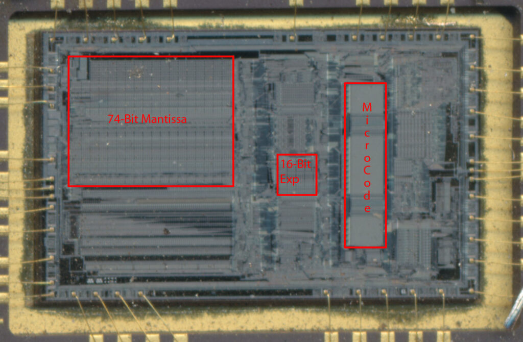
D9008D Die with functional units labeled (will update as I learn more)
Some of the original designers are still employed by NEC (Renesas now) but attempts to contact them have not been successful. Some daring individual may want to try a D9008D in an 8087 socket and see what happens. Electrically, they appear compatible, but the instruction set is certainly different. Finding a new previously unknown vintage chip is quite exciting, but finding one thats related to the x86 architecture is even more interesting. Even after 30-40 years, there are still boards that hold secrets waiting to be uncovered, and thats what make this such an interesting job. The truth as they say, is out there, waiting to be found.
Update: 09/06/2021
I just got brave and threw one of these in a test board with a NEC V30 CPU. The timing might be off a bit as it didn’t want to initially boot, but after a power cycle, the NEC D9008D tests as a working 8087 co-processor, so this mystery FPU supports at least the basic 8087 instructions, and like the 72191 probably adds a lot more.
September 9th, 2021 at 5:09 pm
Some time ago, when trying to find out about the NEC FPUs, I stumbled across a cpu-world forum post from 2009 containing what appears to be a list of the extra instructions that the 72091 was meant to support, in the form of ASM86 assembler macros ( https://www.cpu-world.com/forum/viewtopic.php?t=12863&view=previous ) No ides where that list originally comes from or how legit it is, but doing a bit of checking, the listed instructions at least all appear to fit neatly into 8087 opcode holes (although some of the opcodes have been assigned to other instructions in the i387 and later intel FPUs).
It could be interesting to see how many – if any – of these instructions are supported by the D9008D.
September 9th, 2021 at 5:25 pm
Yup, Elar can’t recall where he found that list, but it includes instructions that were supported by the 72191 and the 80387 so fits well.
I will see about dumping some EPROMs that were with the D9008Ds, in hoe they contain some opcodes we can check.
October 4th, 2021 at 9:24 am
Some documentation can be found in the “MacBus User Manual” by National Instruments, October 1986, pages 3-99ff. There’s also a reference to 72191libcl and 72191asm in it – maybe that’s the source of the assembler macros?
It’s at https://www.ni.com/pdf/manuals/320073.pdf
October 4th, 2021 at 10:09 am
Uup, I hvae that document, and used it some for the article. It shows you how far along the 72191 was along in development at that time.
October 28th, 2021 at 5:56 am
I did some more testing and put one into a Xi8088, after changing the ‘245 for an AHCT family member (the boards you pulled them from are pure CMOS, so we can’t be sure these are TTL compatible). The BIOS detects it as an 8087, but CheckIt fails all tests.
You can see the images at https://imgur.com/a/6K4e546
Mine are NOS, so I think I can exclude defects.
October 13th, 2022 at 3:44 pm
I believe some arcades use some of these chips.
Sega’s model 1 board used a V60 as the main CPU.
1986 Tatsumi Lock-on used a V20.