Processing the Page Turn
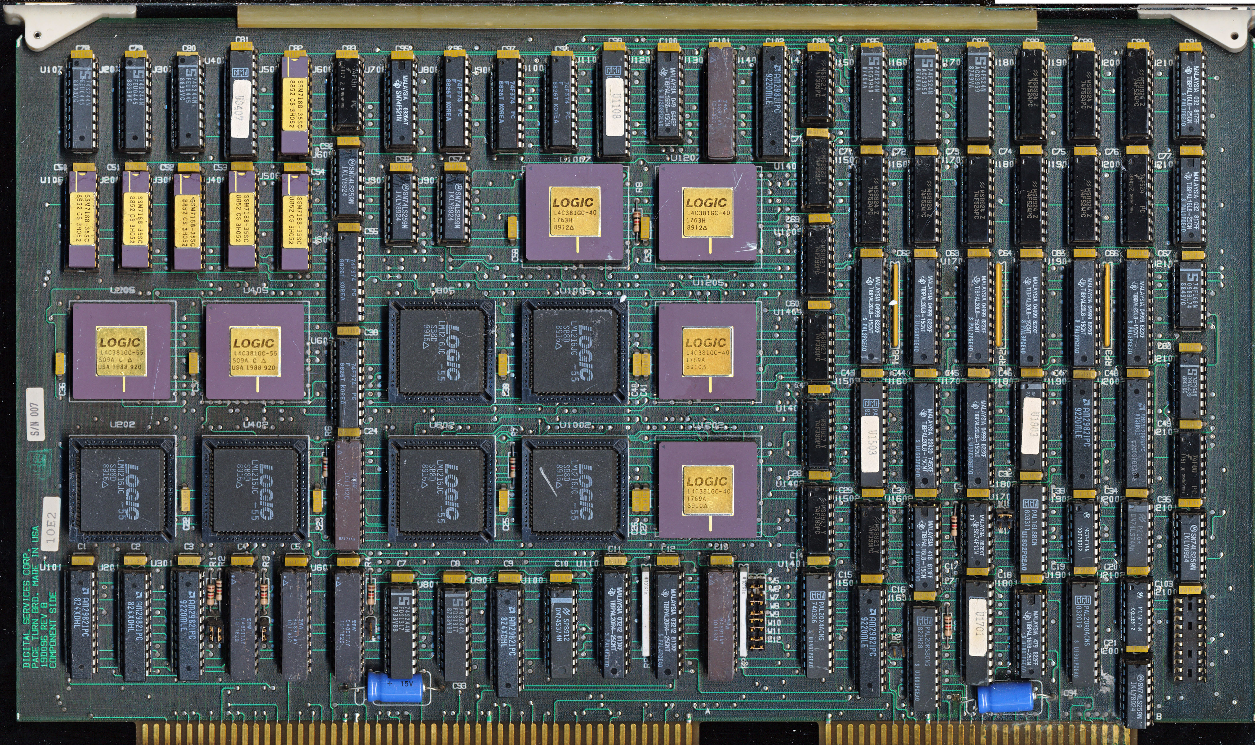
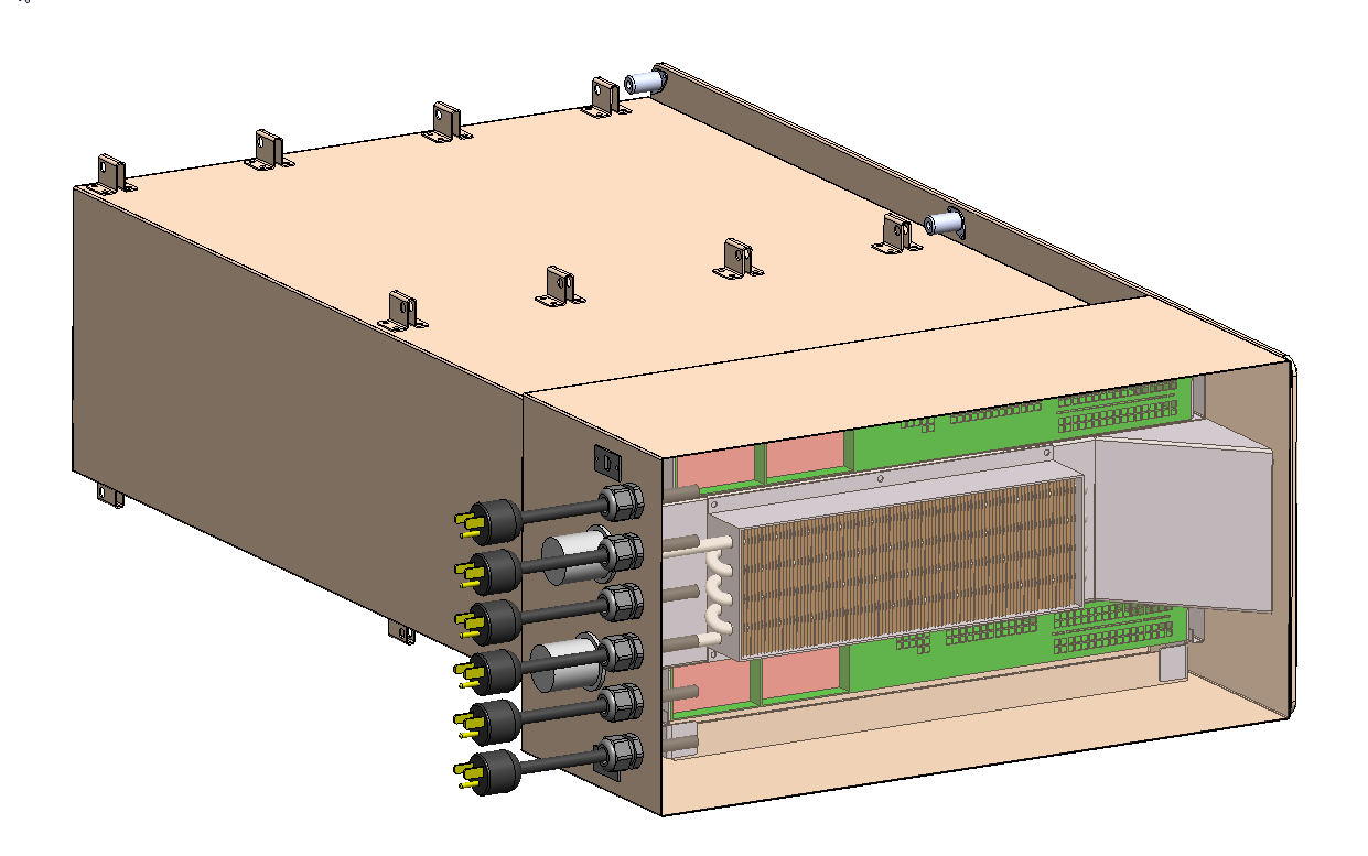
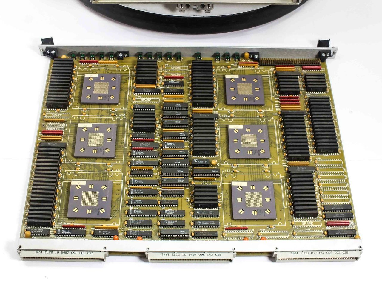
DSC Page Turn Processing Board. 6x 16bit ALUs – 1989
This board isn’t strictly a CPU but it is a processor of sorts. I actually purchased this board as it was described as a DEC board, with not a great picture, having not seen a DEC board with LOGIC ALUs on it I bought it. When it arrived I found it wasnt DEC at all but DSC, Digital Services Corporation. DSC was a video effect company formed in the early 1980’s and later bought out by Chyron, one of the leaders of television video effects hardware.
In the 1980’s, effects on television were generally done in hardware, and required rather specialized hardware for each type of effect. The most primitive were CG (Character Generators) that added captions typically to the lower third of the screen for a broadcast, like the name of the person speaking, etc. As hardware capabilities increased, other effects could be generated, such as a video or image overlay, perspective changes or the page turn effect.
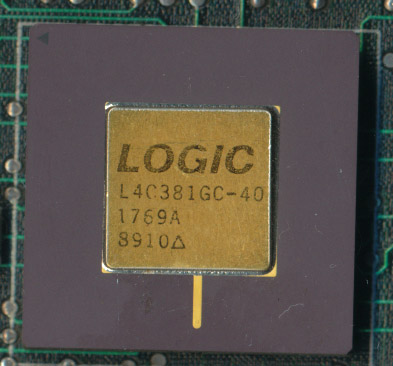
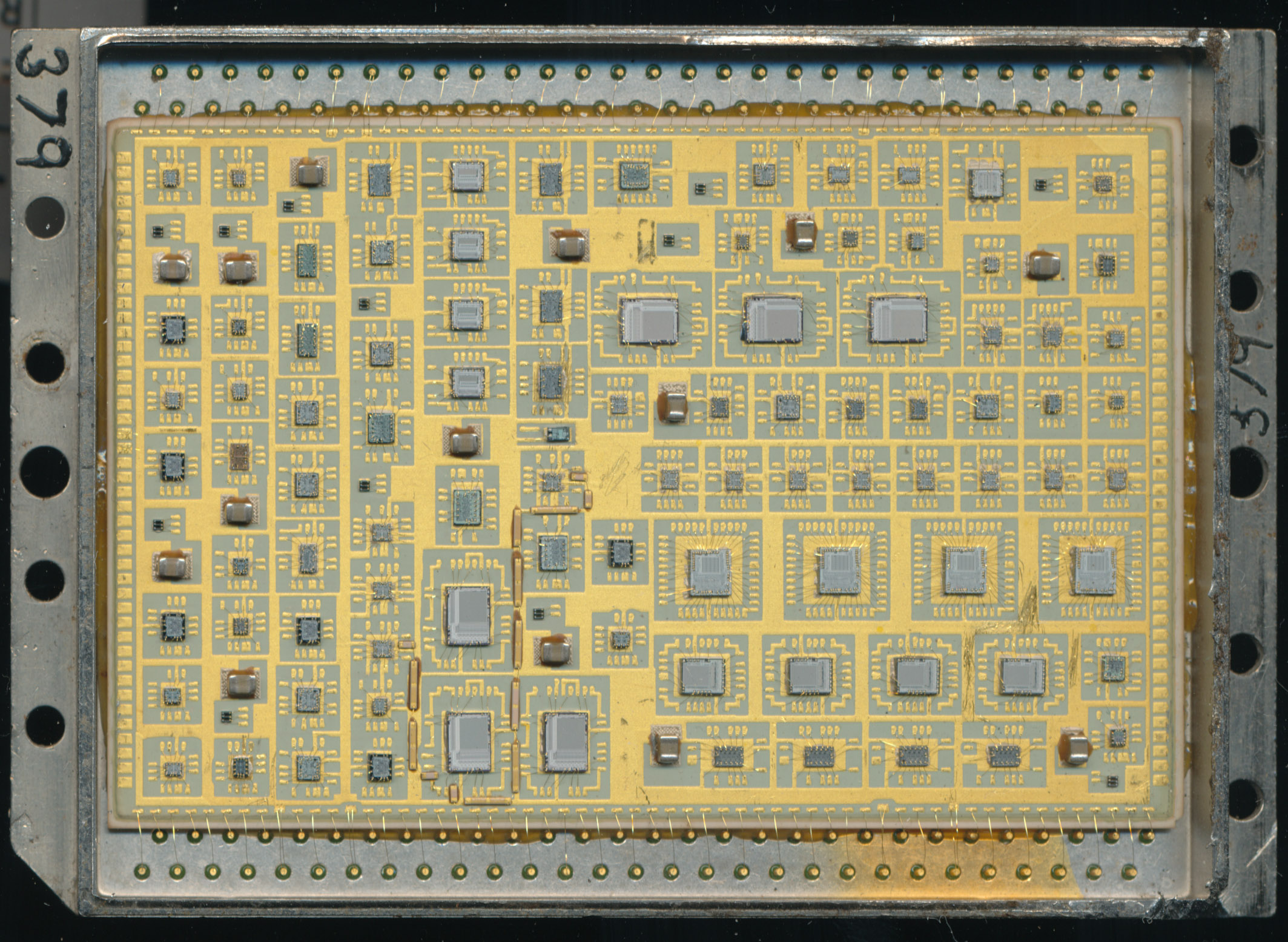
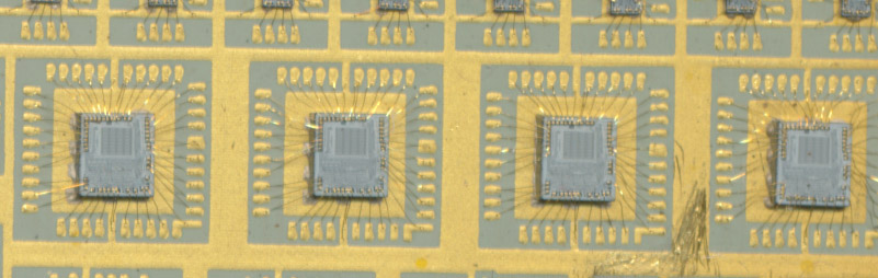
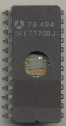
Logic L4C381GC-40 – 4x4bit ALU’s implemented in CMOS
These effects generally were handled by an effects processing system, with each effect having its own board in the system responsible for that effect. Adding an effect required buying an effects board and installing it in the system. This particular board from DSC handles the Page Turn Effect. This is where one video transitions to another video with the look of a turning page. It requires 3 inputs, the first video, the second video being turned to, and a typically solid color/image that represents the back of the page. Here is a quick example on YouTube. Today this can be handled by most any video editing software on a general purpose computer, but in 1989 there wasn’t a computer that could do this in near real time.
This board is built around 6 LOGIC L4C381GC-40/55 ALUs and 6x LOGIC LMU216JC-55 Multipliers. The 4C381s are a 16-bit CMOS ALU, based on 4 74381 4-bit ALU,s a Carry Generator and interface logic. Basically 1970’s technology updated to CMOS. They handle 16 bit Addition, Subtraction and basic logic (XOR/OR/AND). The LMU216s are 16 x 16-bit Parallel Multipliers. They are the equivalent of the old AMD Am29516 that was cloned by TRW, Cypress and IDT.
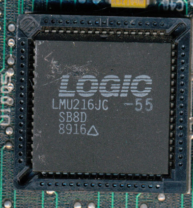
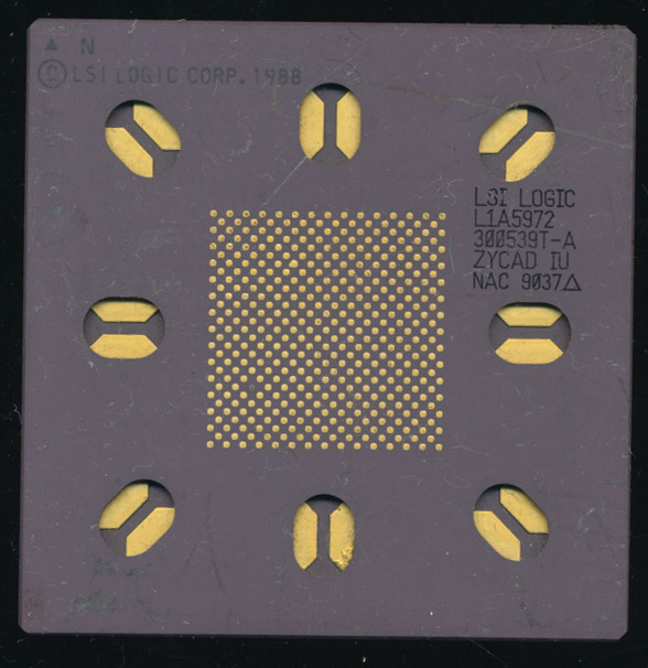
LOGIC LMU216JC-55 – 16×16 CMOS Multiplier
The rest of the board consists of 6x64Kb or Video RAM, shift registers, and all the control logic (in PALs) to provide the instructions for the ALUs and multipliers. The arrangement of the board suggests a 64-bit computation section and a 32-bit section. Just as in the 1970’s the ALUs and multipliers have been used to make a custom processor, with a very specific instruction set and purpose and do so at a speed that would be compatible with broadcast television. Sitting on one’s couch in the 1980’s watching TV and seeing a cool page turn effect one would think, ‘Hey that’s cool!’, yet have no idea that an entire processing system had to be designed, built and coded for that one second of television.
Russian Translation now available here by Vlad Brown