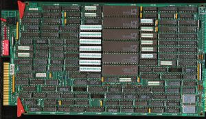
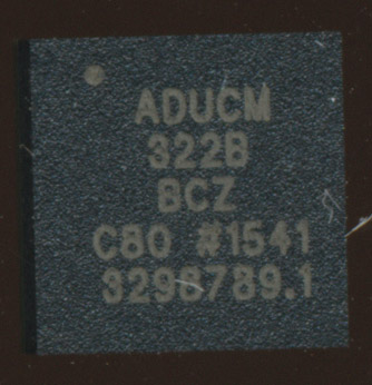
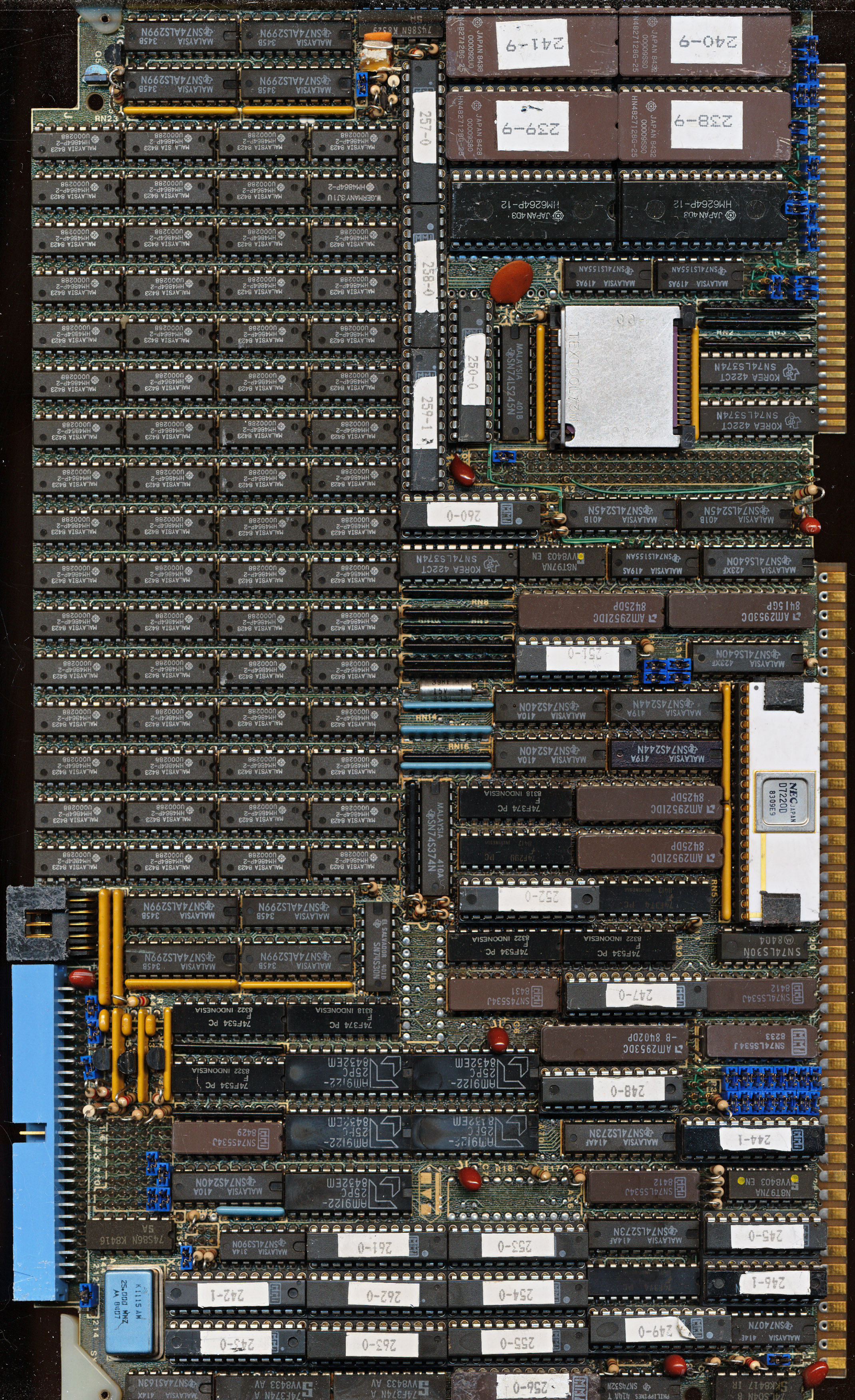
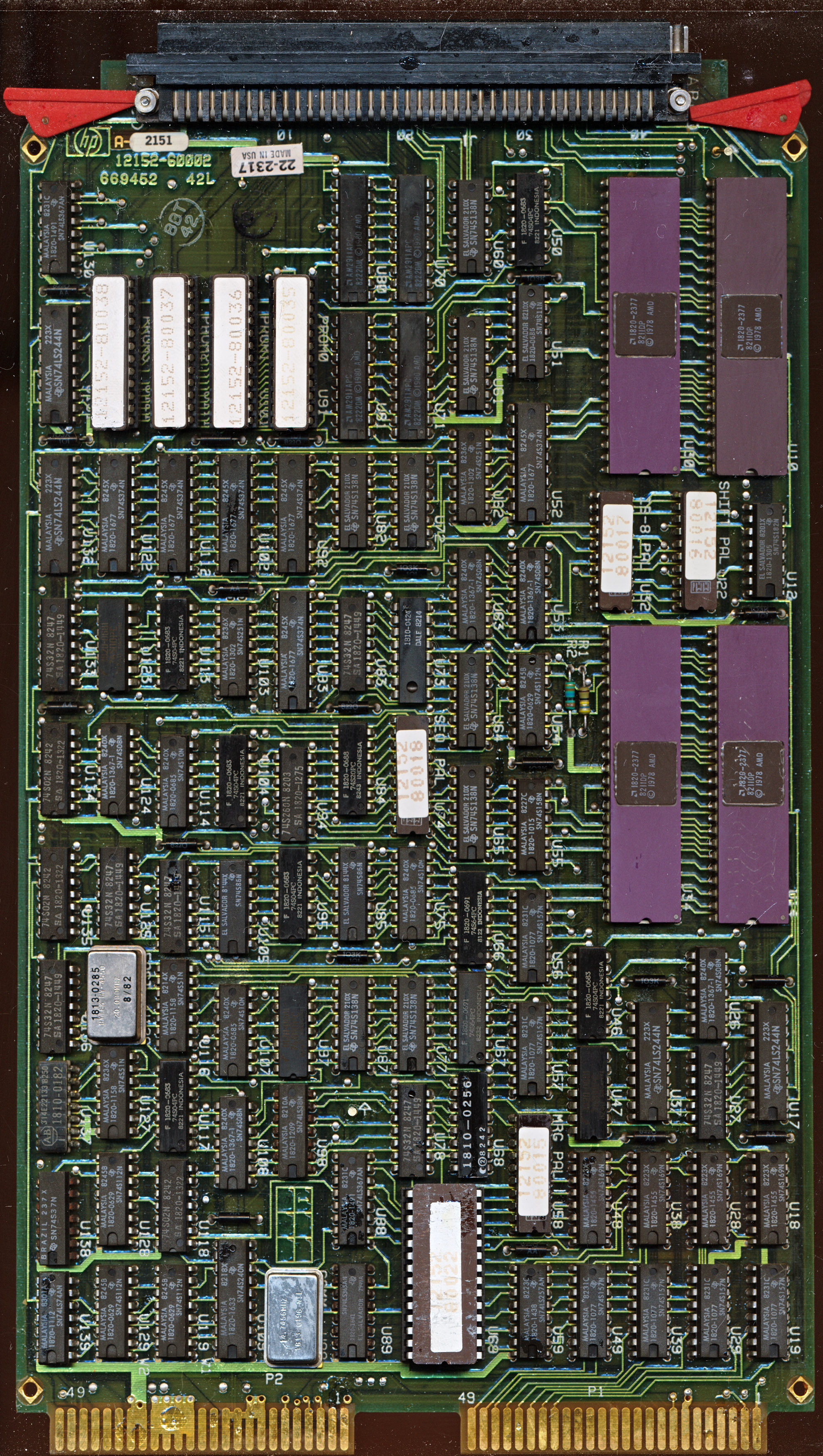
HP A600+ Processor Board. 4x AMD AM2901CDC (1820-3117) 1x AMD AM2904DC and 1x AMD AM2910 (1820-2378). Some versions used 2901’s from National Semiconductor.
In the early 1960’s HP was exploring connecting computers to its various instruments, for control, monitoring, and logging. The DEC PDP-8 had come out in 1965 as perhaps the first mini-computer and could be used to control HP’s instrument’s. However, HP determined that it would actually be easier, and faster to design and build their own computers rather than work with DEC. DEC probably didn’t see HP’s interest as important enough to make it easy (some interfacing for I/O etc would have to be done). It worked out well for HP however, as this pushed them into an entirely new, and emerging market.
In 1966 HP released the 16-bit HP 2100 (later to be renamed the HP 1000 series). It was a design that had begun under Union Carbide’s Data Systems Inc, a company HP had recently acquired. This gave HP a head start, and allowed them to evolve the design to meet their needs (at the time mostly to control instruments). When released it included not only the hardware but a completely function software suite as well, including a FORTRAN compiler. They initially ran with a 10MHz clock and a 1.6usec memory cycle time.
Throughout the 1970’s the design evolved, and would lead to many computers. The 98xx desktop systems using HP’s NMOS BPC Hybrid processor were based on the HP 1000 series. The design was a fairly simple accumulator based architecture with 2 16-bit accumulators (A and B) and a 15-bit PC and 68-base instructions. The first version was directly programmed but all subsequent versions were microprogrammed, making alterations and additions to the instruction set much easier, a feature that became important in keeping the HP 1000 around.
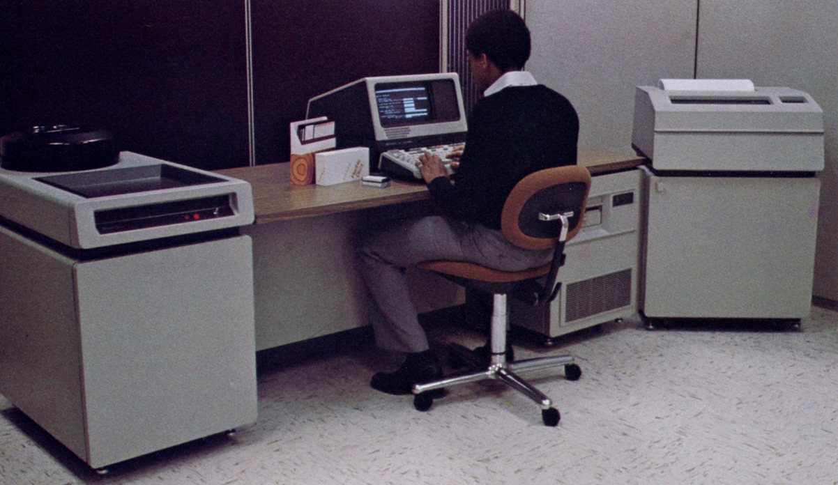
The A series were the HP 1000’s of the 1980’s. Development began around 1980 and the first computers, the A600 and A700, were released in 1982. These were some of the first LSI based processors for the line. THe A600 processor was called the ‘Lightning.’ The name “Lightning” came from the Mark Twain quote “Thunder is good, thunder is great, but it is lightning that does all the work.” “Thunder” was a reference to the PDP 11/23, one of DEC’s newer machines at the time. HP had went from considering using DEC’s computers to run instruments, to the 4th largest maker of such computers in only a decade. Certainly a fact not lost on either company.
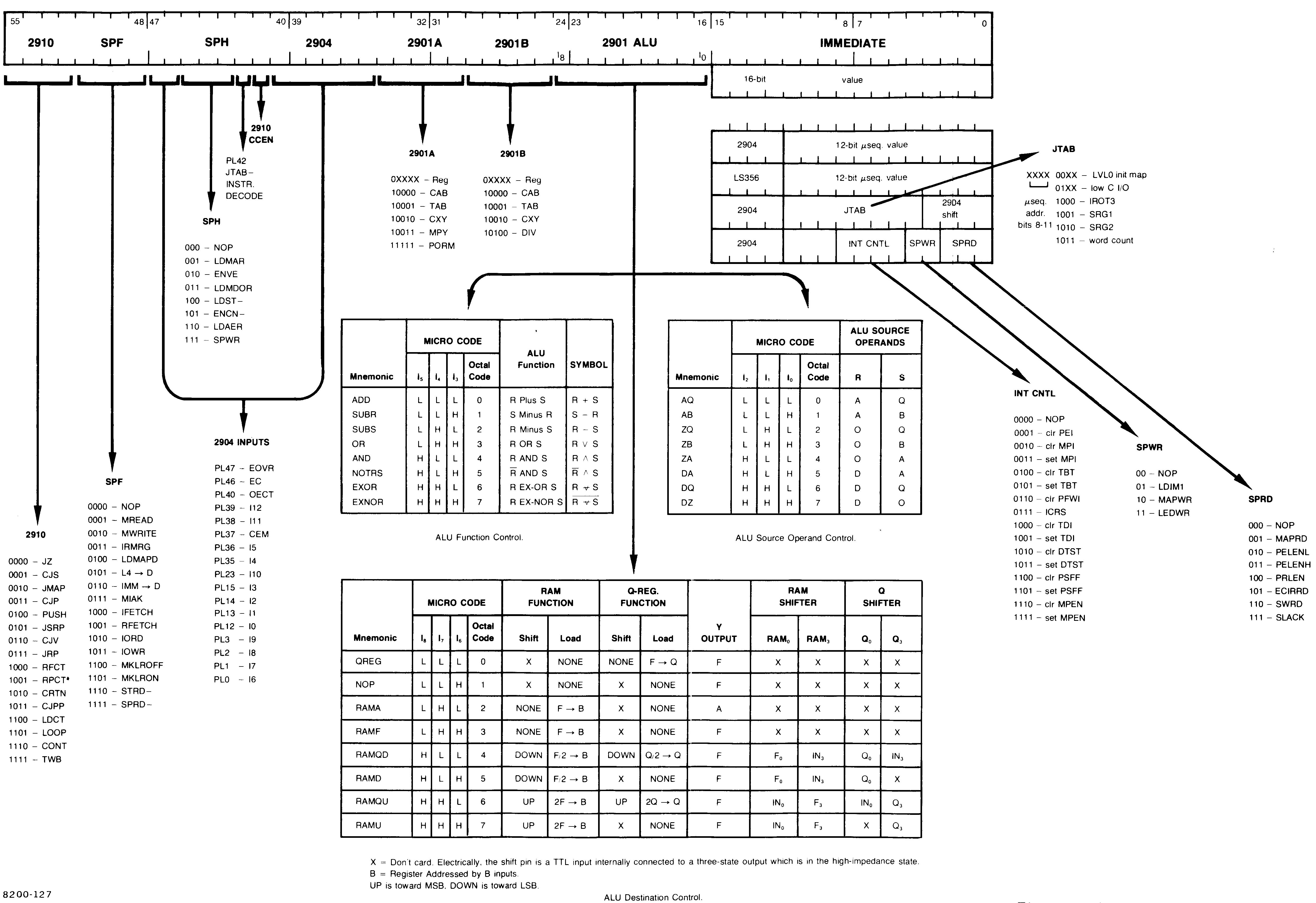
The A600 is an interesting design, it is of course microprogrammed, and is based on AMD AM2901B bit-slice processors, supported by a 2910 microsequencer, and the 2904 status/shift control unit. The rest of the board is Schottky TTL, PALs, FPLAs. and ROMs. Each HP 1000 instruction is microcoded into a 56-bit instruction for controlling the 2901’s 2904 and 2910. These 56-bit instructions directly operation on the processor. Certain bits interface with certain parts of each chip, so they are directly executed.
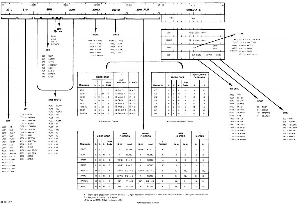
A600 – 56-bit microinstruction word directly operates on the hardware (click for LARGE version)
A series of PAL’s contain the microcoding, allowing for easy updating (at the time). A standard A600 executed 182 standard HP 1000 instructions. It could do so at a rate of 1 MIPS, with a cycle time of 227 nanoseconds.
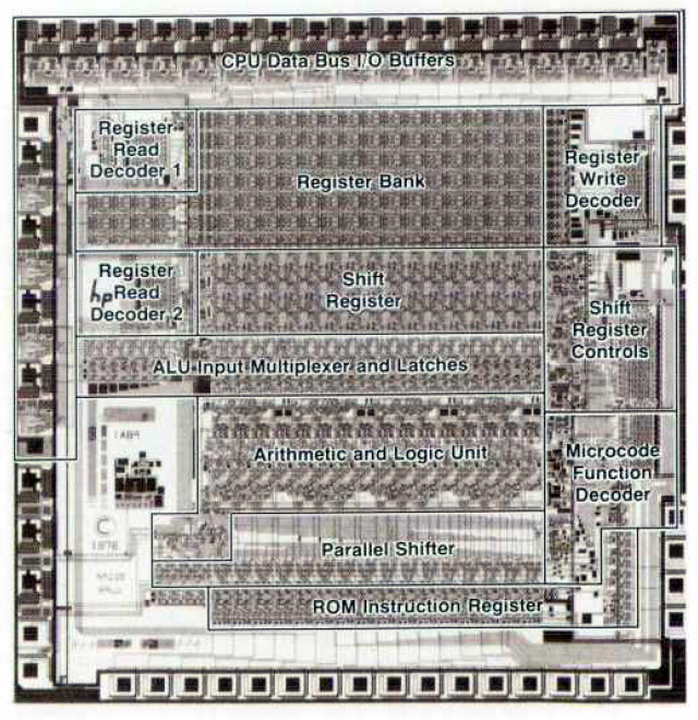
Each 2901 is a 4-bit slice processor, and contains 4-bit registers and ALU’s. The HP 1000 A and B registers are mapped directly to the R0 and R1 registers of the 2901’s and the Program counter resides in R15. The PAL’s determine what HP 1000 instruction is being executed, and decode it into the proper 2901 assembly code, building the 56-bit instruction word. This is one of the best examples of how the AMD 2901 (and other bit slicers) were designed to be used. The end user has no idea, or need to know what is executing their HP 1000 code. Its is decoded and send to the bit slicers for processing which then return the results to the proper place. If new functions are needed a new processor does not need to be designed, simply add additional PAL code to decode the new instructions. And that is exactly what HP did….
Read More »


