How to 386 Your AT: Intel Inboard 386/AT
With the release of the 32-bit Intel 386 processor in 1986, owners of IBM PC/XT and AT type systems (8088 and 80286 systems) were left a bit in the dust. This was a concern (or opportunity) for Intel as well. They designed an upgrade solution at the same time as the 386, to be able to be used in the now obsolete computers. This was the Intel InBoard 386 series of upgrade cards.
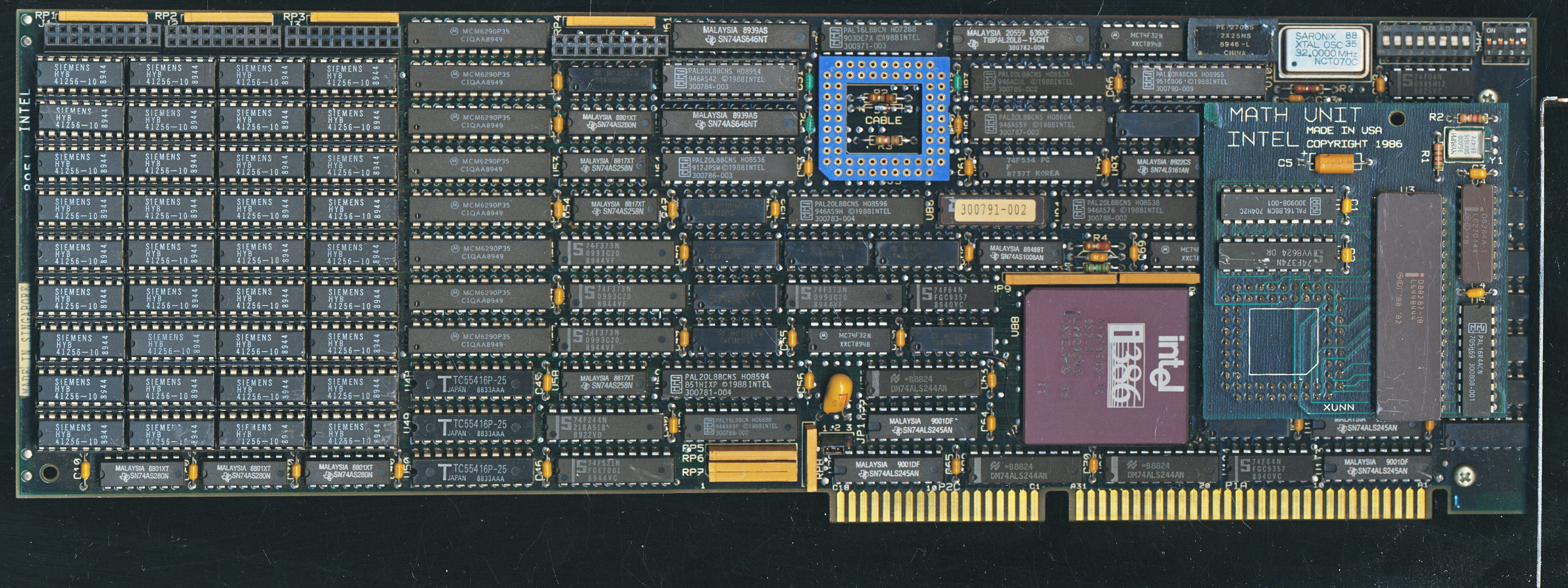
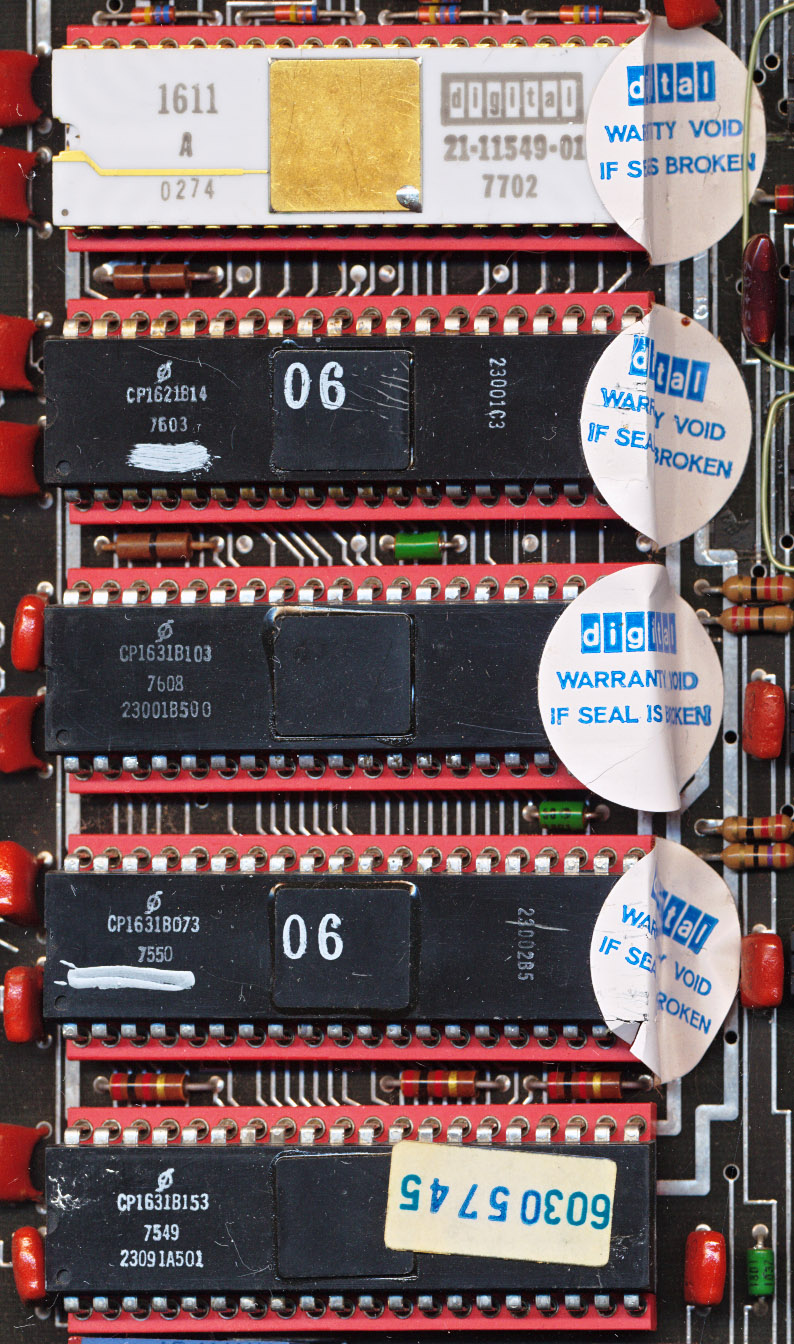
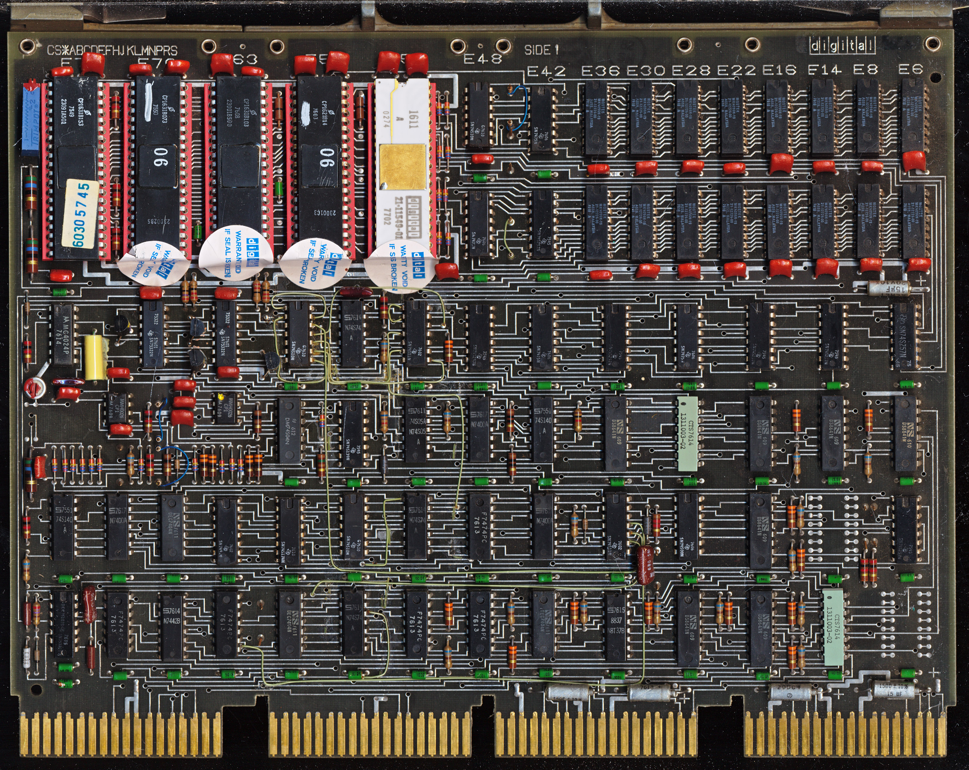
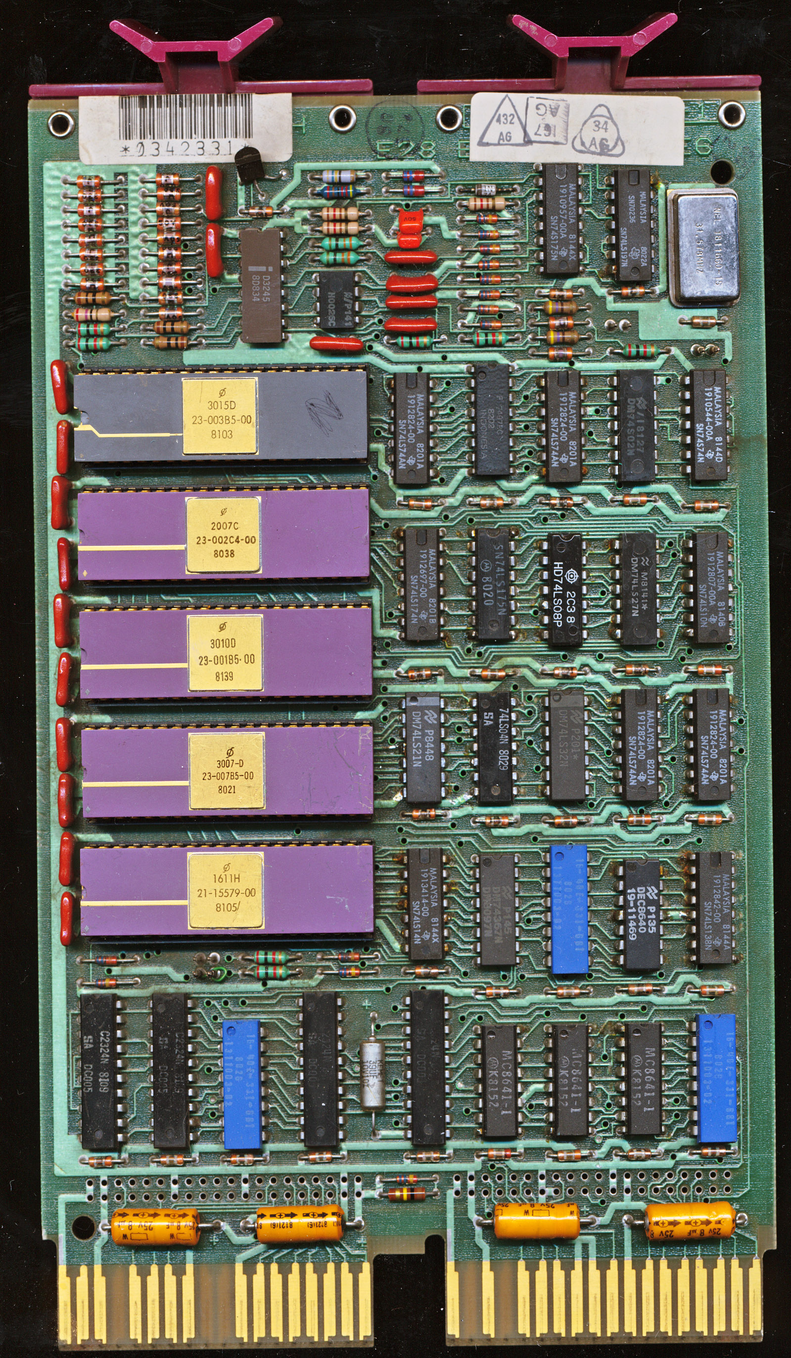
InBoard 386 AT with 1MB of RAM and 80287 FPU Option (very unusualy on a late model Inboard, this one from 1990, but the FPU is from 1986)
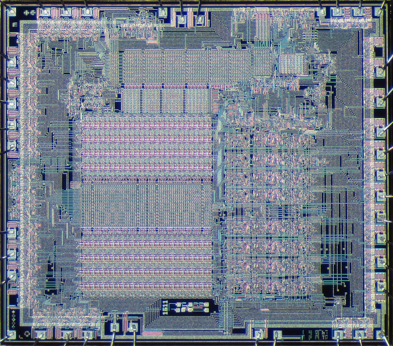
The InBoard, as its name implies, was a internal 16-bit ISA card that was used to upgrade these systems. It included a 386DX processor running at 16MHz, 64K of cache, and (optionally) 1-3MB of additional RAM. Two version of the board were made: the PC/XT version was designed for 8088 processor based systems, and the AT version was for the 286 systems. These boards required the removal of the original processor, and then a cable was ran from the old CPU socket, to the the InBoard 386 board. On system start up the original BIOS booted the system, and loaded the DOS operating system. The config.sys file would then call on the drivers to load the InBoard 386 specific features. The original system was essentially unaware of the new processor, instructions were executed by the InBoard transparently.
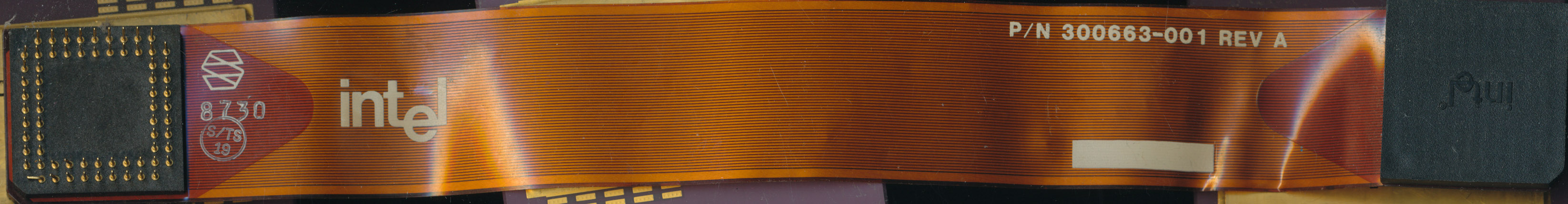
Flat Ribbon Cable used for connecting the board to the old CPU socket. If the cable could not reach the socket, your system was not compatible. Cable length was restricted by signal timing, rather then the common complaint of Intel being ‘stingy’
Early AT systems used a 6MHz CPU and ISA bus speed, so Intel provided a 8MHz crystal to replace the original on the motherboard. This ensured the ISA bus that the InBoard used to communicate with the original memory and peripherals ran fast enough and did not become such a huge bottle neck. The base model InBoard did not come with any RAM, it could use your existing system RAM just fine. Adding RAM, however, was a worthwhile upgrade. The Board itself supports 1M (36 100ns 256 kbit chips, including parity) and a daughter card could add another 1M or 2M. This RAM was accessed via the 80386s 32-bit address bus so was much quicker. It also was a single wait state access. You could configure the InBoard to backfill (take over for) your existing system RAM, at least down to 256K, so that the computer would only use the first 256K of the slower RAM before moving to the RAM on the InBoard. If your system had 512K of RAM you would ‘waste’ half of it but at the benefit of much faster access times. The Inboard 386 had another trick up its sleeve to improve speed…
Posted in:
Boards and Systems