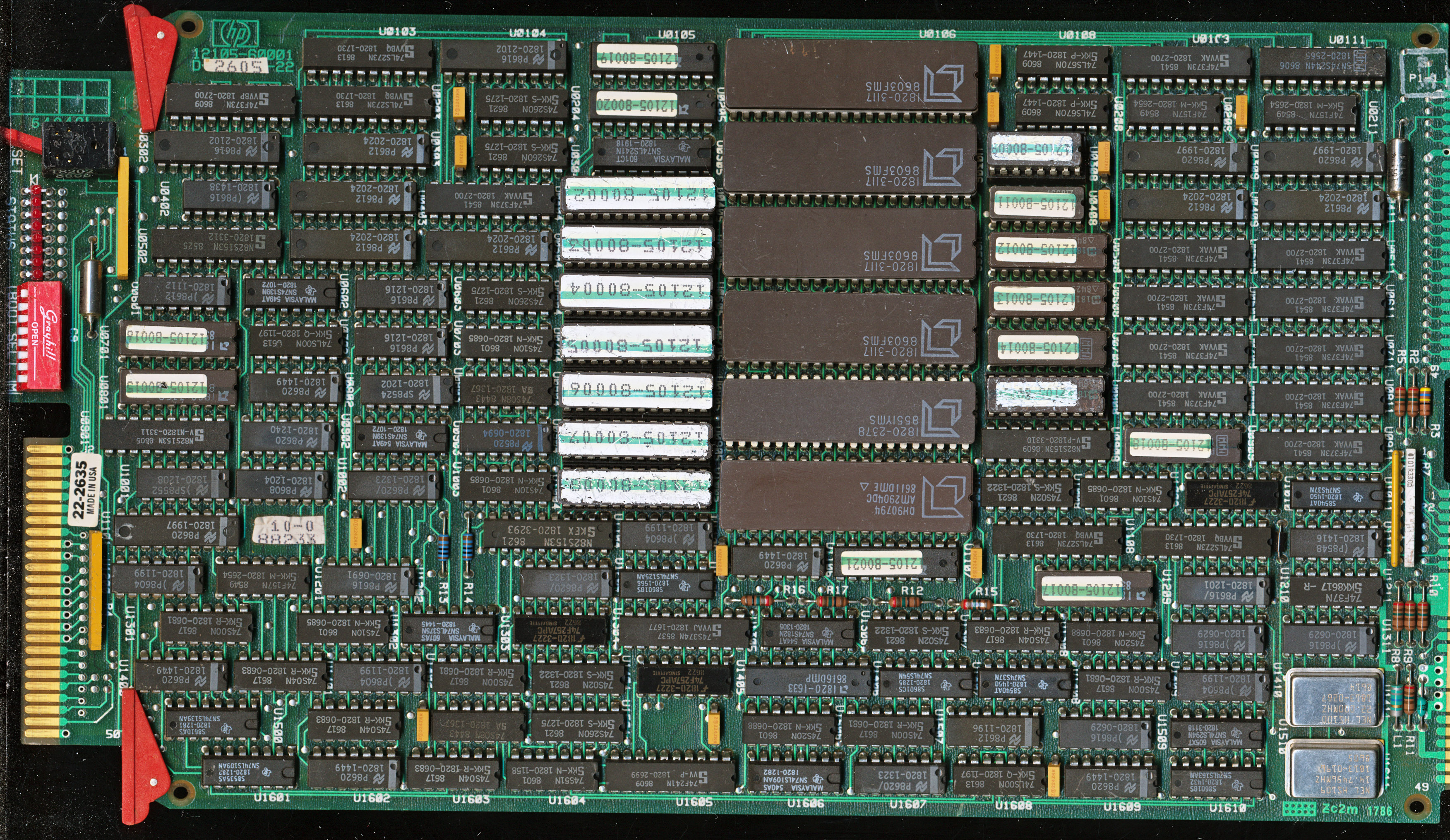
Matrox SX-900: x86 Accelerated GPU
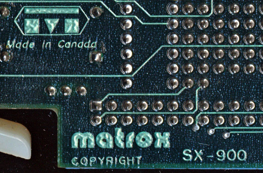
Matrox SX-900: Serial# 266 – Nov 1984
In today’s age of GPU’s the GPU is often used to offload the x86 processor. Many tasks are well suited for the thousands of GPU cores on modern graphics cards, tasks that would be a large burden on an x86 processor. In 1984 though, Matrox took a different approach to high-end GPU design. Matrox was founded in Canada in 1976, and has been making graphics cards since they first released the S-100 bus ALT-256 in 1978. Matrox kept up with the hardware changes of the time, released MULTIBUS boards, Q-Bus boards, and eventually PC compatible cards.
The SX-900 was the value (around $2000) version of their 2 board GXB-1000 (that was $3000-4000). The Matrox SX-900 was a standard MULTIBUS card with support for 640x480x8bit graphics. It supported a fill rate of 20 MPixels/sec which was very impressive in 1984. By comparison, the Nvidia NV1 (STG-2000) released in 1995, was only capable of a 12MPixel/sec fill rate, albeit at a richer color depth. So how did Matrox, in 1984, achieve such performance?
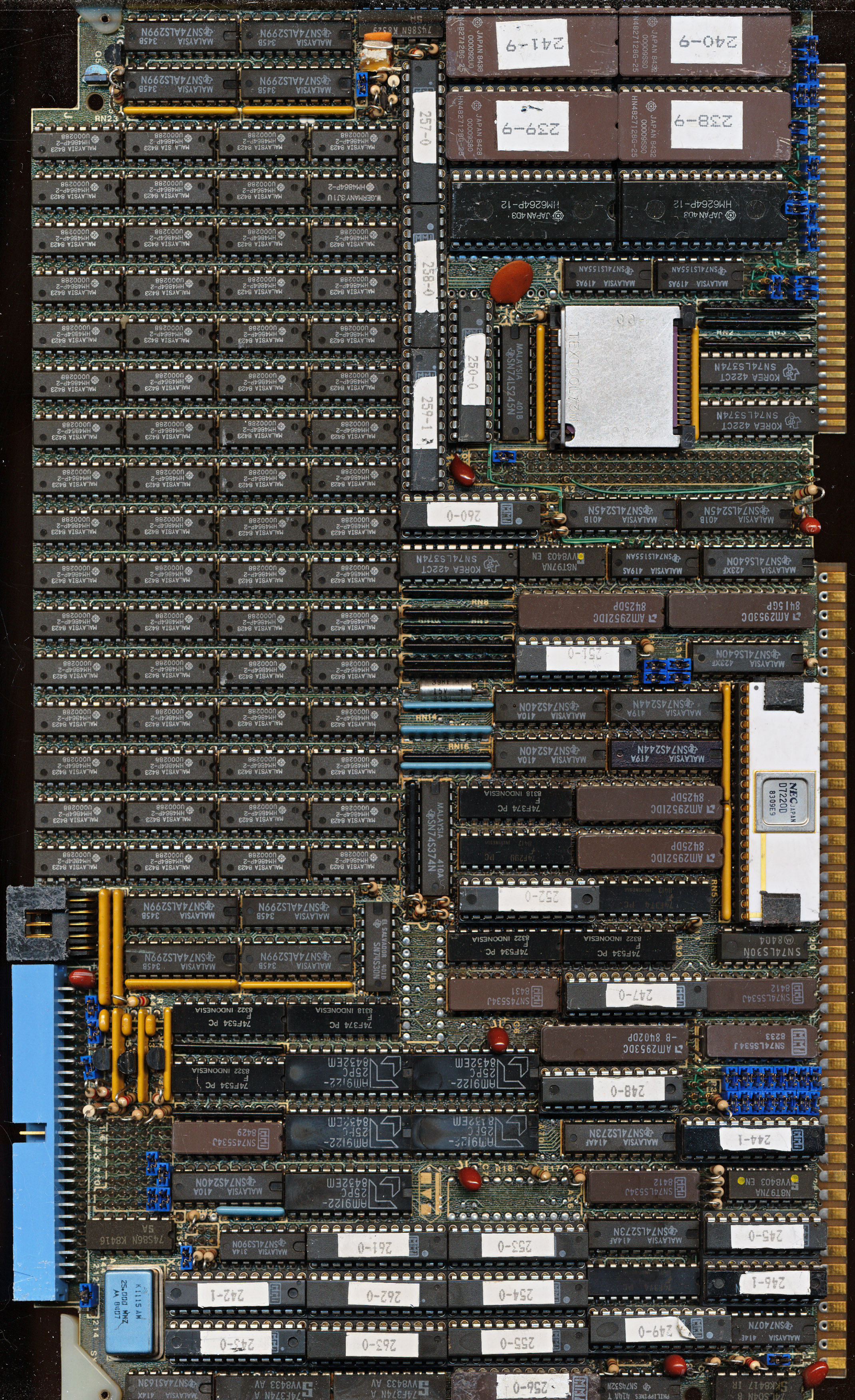
Matrox SX-900: Powered by a 80286-4 Processor and upD7220 Graphics Primitives Processor
Matrox used an Intel 80286 processor, running at 4MHz (the slowest 286 made) as a Display List Processor. It handles all high level commands (256+) and then controls the rest of the cards hardware, including the NEC uPD7220 Graphics primitive processor and a advanced pixel processor (implemented in PALs/TTL). Together they bring rather impressive performance. The board supports up to 4096 colors (in a Lookup Table) but can only display 16 at a time. Interestingly the board has 512K of 150ns DRAM for use as video memory, more than enough for 640×480 graphics. Also included is 640 bytes of 25ns ECL SRAM (5x AM9122-25PC), and 16K of 120ns CMOS SRAM implemented with 2 HM6264s. Firmware (the same firmware used for the GXB-1000) is held in 4 27128 EPROMs for simple updating as needed.
The SX-900 was used in CAD systems, industrial automation, processor control, and other applications where data needed to be shown the user graphically, rather then on a green glowing monochrome text display. One of the more famous applications was the University of Milan (in Italy) where the SX-900 (supported by Intel iSBC286 computing boards) controlled the K800 Superconducting Cyclotron, a 100MeV particle accelerator. THis cyclotron ended up being moved and completed at Catania, also in Italy.
Many of these boards are still in use, dutifully displaying graphics and providing user interfaces to thousands of processor control systems in factories and institutions around the world.
Posted in:
Boards and Systems