June 12th, 2019 ~ by admin

Xeon Overclocking: Making Gallatin Gallop

This article is part of The CPU Shack’s continued partnership with guest author max1024, hailing from Belarus. I have provided some minor edits/tweaks in the translation from Belorussian to English.

If you still remember the times of the Pentium 4 running on Socket 478 with the Northwood, Prescott and Gallatin cores, then you should remember what about these processor cores were different from each other. Northwood was fast like a mountain doe due to a shorter 20-stage pipeline that allowed it to perform many operations very quickly without tremendous losses due to branch mis-predictions etc. , but inferior to Prescott frequency potential in overclocking, which in turn was as strong as a buffalo, due to twice the L2 cache memory(1M vs 512K) and finer tech process (90nm vs 130nm). But like any hoofed animal, it was not agile, to achieve the higher clock speeds its pipeline was extended to 31-stages, resulting in some cases, clock for clock out performing Northwood, But doing so at the expense of much heat.

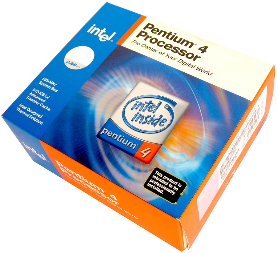
A separate niche in the food chain was occupied by “Gallatin”, which combined the properties of the two previous iterations, a shorter 20-stage pipeline, with the high clock speed of the Prescott, but in its arsenal it also had a very formidable weapon, which was the presence of an additional L3 cache of 2 MB. The price of ownership of this “beast” was high, and in the literal sense of the word, it was equal, like any other representative of the Extreme Edition series – $ 999. I resisted this extreme processor, choosing  hero from AMD, the FX-51, which I consider to be one of the most outstanding processors of all times and peoples.

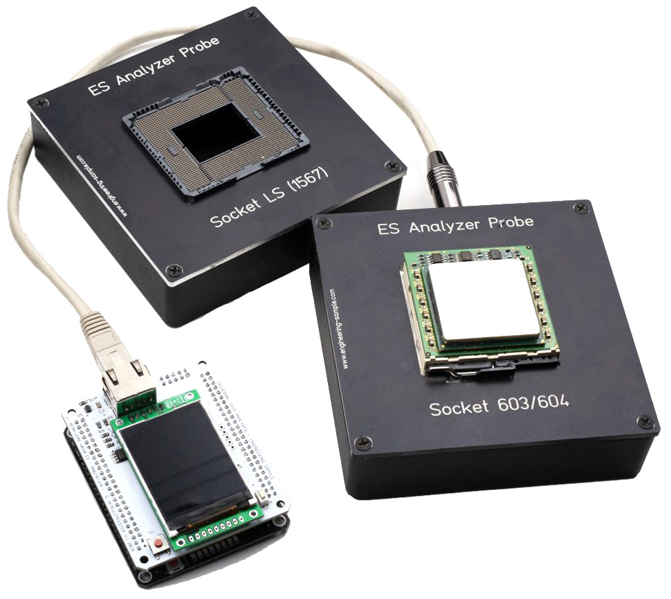
Xeon Universal Chip Analyzer by x86.fr

What could be better, cooler or faster? I’ve been looking for an answer to this question for a long time, until I became acquainted with the Intel Xeon server processors on Socket 604 and in particular with processors based on the Prescott 2M core, which have twice the cache size compared to their desktop counterparts and can run on ASUS production boards.

As everybody knows, it is the advanced desktop flagships of both processor manufacturers that originate from the server segment. So from the Opteron’s turned out the AMD Athlon FX-51, and from the Intel Xeon MP – the Pentium Extreme Edition. This parity of events has been preserved until now.
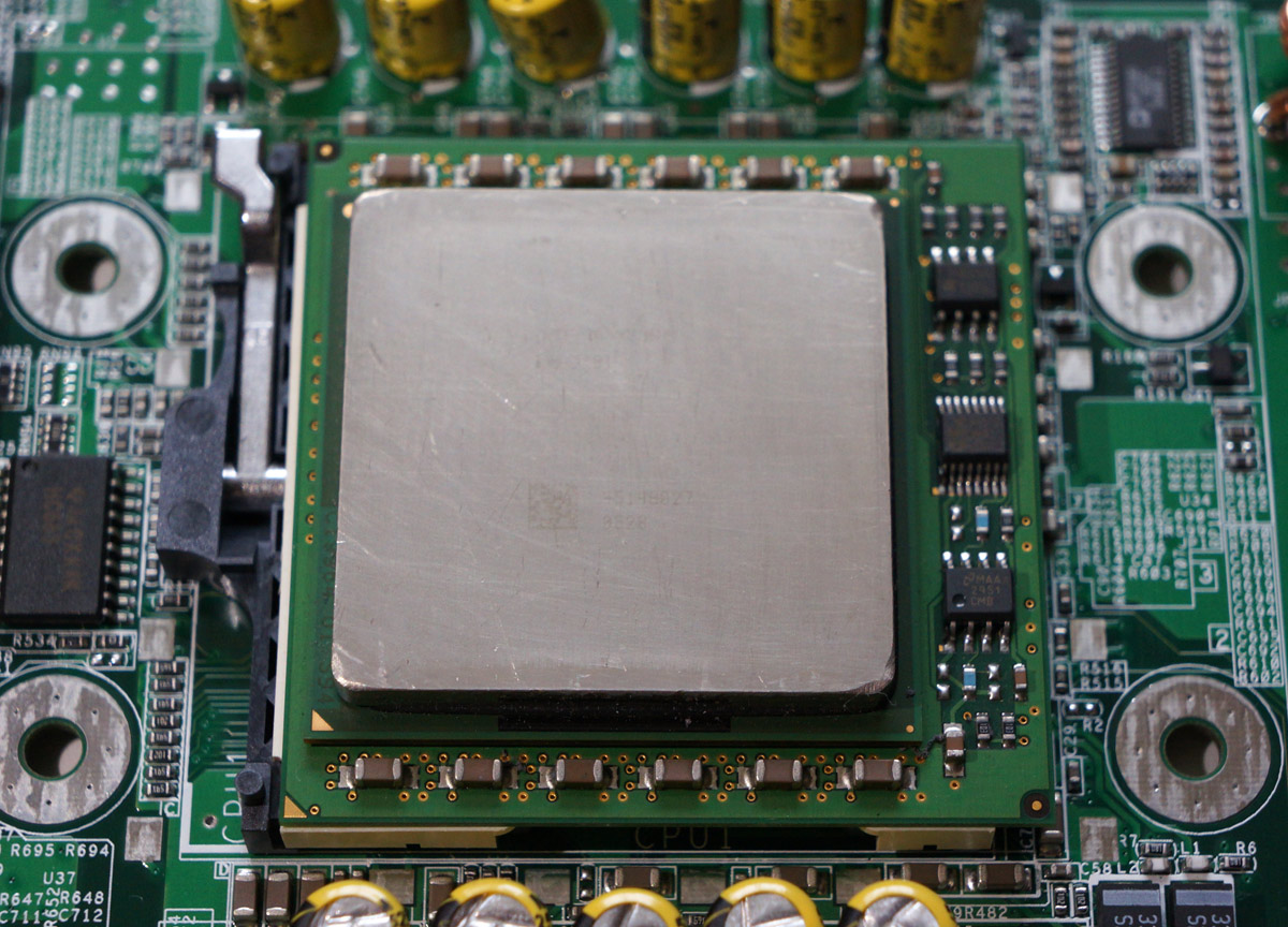
Xeon Gallatin MP

The server representatives of Intel Xeon processors on the Gallatin core are divided into two branches: Xeon MP (Gallatin) and simply Xeon (Gallatin). The differences are in the number of simultaneously supported processors in the system. So Xeon MP supported running up to four processors  usual Xeon could be installed in servers only in pairs. There is also a difference in steppings of the processor core itself. Let me remind you that the desktop version of “Gallatin” were the M0 stepping, just like the regular Intel Xeon series.

The Xeon MP line, by contrast, is based on an earlier stepping from A0 to C0. Among the representatives of M0 stepping, you can find four Xeon models (Gallatin) with 1M of L3 cache, with frequencies from 2.4 GHz to 3.2 GHz, and one model with a doubled  L3 cache to 2 MB, pretty much the same as a Pentium 4 Extreme Edition. This model gave rise to the first “extreme” Pentium.

Read More »

August 15th, 2018 ~ by admin

CPU of the Day: The 61 Knights of the Intel Xeon Phi

Xeon Phi – Knights Corner – Engineering Sample

In June of 2013, 20 years after the release of the Intel Pentium Processor, Intel released a new processor, technically a co-processor that Intel referred to as a MIC (Many Integrated Core).  It was branded as a Xeon, specifically the Xeon Phi 7000 series but at its core, it was nothing like a Xeon of 2013.  Code named Knights Corner, it built on the Knights Ferry.  Knights Ferry used many Larrabee GPGPU cores and was not designed as a commercial product.  Knights Corner , however, was, and to do so, Intel stuck with an architecture that customers were very familiar with, x86.  The Knights Corner integrated 61 Pentium P54CS cores onto a single chip.  The original Pentium P54CS was made on a 0.35u process and topped out at 200MHz.  They included 16K of L1 cache on die, and typically 256-512K of L2 Cache off chip.  The implementation of the Pentium on the Phi gets a bit of an upgrade.  The cores are made on a 22nm process (16 times smaller) and clocked at up to 1.2GHz.  L1 cache has been increased to 64K per core (32K Instruction  32K Data).  L2 cache remains at 512K

Knights Corner Die. – 62 Cores – 8 GDDR5 Memory Controllers

per core, but at 22nm, integrating all 30.5MB of cache on the same die becomes relatively easy.  The biggest change to the cores is adding support for 64 bit instructions, as well as adding a new execution unit called the VPU. This VPU (Vector Processing Unit) has its own 512-bit wide SIMD instruction set, integer support, Fused Multiply/Add, and other advanced features that are more commonly found in GPU’s. The VPU is the result of Intel’s work with Larrabee, the precursor to Knights Corner.  Interestingly MMX/SSE are not supported by the cores natively, this is handled in software (using virtualization) and leveraging the VPU included with the 61x Pentium Cores.  With the VPU, each core has 4 execution units (VPU, FXU, and 2 x Integer units). This allows the cores to support 4-way multi-threading; in practice, 2 threads are most common as 2 execution units are usually tied up calculating memory addresses.

Knights Corner Sample – This is a 1.09GHz part while production versions were bumped to 1.1GHz – Elpida 2Gbit GDDR5 RAM chips surround the core.

For some reason Intel was very vague about information on die sizes/transistor count on the Phi.  Many sources claim 350mm2 die with 5 Billion transistors.  Taking apart a Phi shows that the die is actually much larger.  In fact the Xeon Phi die is 705mm2 and has 5.1 Billion transistors.  A 22nm Haswell Xeon with 18 cores has a die area of 622mm2 containing 5.6 Billion transistors. This means the Xeon Phi die wasn’t the most efficient is its use of space, likely due to the amount of room needed for the very large rings used to connect all the cores.  Looking at the die you can also see a lot of unused space.   There are actually 62 cores per die (with only 61 used max.)  This means 31MB of L2 cache which at 6 transistors per cell (bit) accounts for 1.5 Billion of the transistors.  L1 Cache is 64K per core so another 190 Million transistors there.  That leaves the bulk of the die for the cores, memory controllers, and the 3 interprocessor communication rings that handle communication between cores, MC’s (8 GDDR5 Memory Controllers per die), and the outside world.

Each Xeon Phi board includes the processor, as well as 6-16GB of GDDR5 Memory (8GB on the Engineering Sample here).  Memory is handled by 32 Elpida EDW2032BBBG-6 2Gbit GDDR5 6 Gbps chips. This gives the card is 352 Gbps memory bandwidth and 1 TFLOPS of computing performance.  All in a PCI-E car that dissipates around 300W.   Card/System management is provided by a NXP LPC2365FBD100 72MHz ARM7TDMI processor.

Knights Corner Xeon Phi with cooler removed. 16x 2Gbit GDDR5 (+16 on the back)

In January of 2013 the Texas Advanced Computing Center in Austin, TX announced the Stampede Supercomputer, the first large scale deployment of Xeon Phi Processors.  It used 6880 of them in its 6400 compute nodes and could hit nearly 10PFLOPS of performance. In June of 2013 the Chinese supercomputer Tianhe-2 became the fastest supercomputer in the world, a title it held until the end of 2015.  It was powered by 32,000 Intel Xeon E5-2692 2.2GHz 12C Ivy Bridge processors and a massive 48,000 Xeon Phi co-processors resulting in over 33PFLOPs.

Tianhe 2 Super Computer with 48,000 Knights Corner Processors.

Intel made a successor to Knights Corner, known as Knights Landing, that was based on the Atom core, but then began to wind down the project.   Avinash Sodani, chief architect of the Knights Landing chip took a job at Cavium Networks (who make multicore MIPS networking processors), and Intel then hired Raja Koduri, the chief architect of AMD’s GPU processors.  Intel’s future seems to be one based on Xeon, and GPU’s.

Like the Knights of old, the the Xeon Phi has been passed up by other technologies, certainly still useful, but destined to the halls of museums and history books.  It came, and it conquered the Top500 Supercomputer list, and then quietly fades away.  On July 27th Intel quietly announced the discontinuation of the Xeon Phi line, with last orders accepted the end of this August (2018).