The History of Angstrem Memory IC’s in the USSR
This article is about memory chips manufactured by one of the entities – the leader of the electronic industry of the USSR – Angstrem. As you know, the Soviet Union ceased to exist in December 1991. We restrict ourselves to the development period of the considered memory chips produced at Angstrem, the end of 1991. Let’s make an attempt to track how the capacity of memory chips grew, how technologies were improved that allowed the Soviet Union not to let the world leaders in electronics go far from itself at that time. A small example: Angstrem’s Dynamic RAM 4K went into mass production in mid-1975, Intel introduced its own in 1974. Intel launched a 16K DRAM in 1977, and Angstrem released its counterpart in 1978.

Angstrem Headquarters
Angstrem was established in June 1963 in Zelenograd (outside of Moscow) as a pilot plant in conjunction with the Scientific Research Institute of Precision Technology. At Angstrem, new technologies for the production of microelectronics were developed, and pilot batches of new microcircuits were also produced. The debugged production technology was then transferred to other enterprises of the USSR and countries of Eastern Europe.
The development and manufacture of memory chips was one of the main activities of Angstrem. It was on them that new semiconductor structures and production technologies were more effectively worked out, and the stability of obtaining finished products is considered in world electronics as a sign of technology ownership. It’s relatively easy to make a small batch of good chips, it’s hard to make a process whereby a large amount of chips can be made and be reliable. It was the very low chip yield percentage that played a cruel joke on Angstrem when mastering the production process of the DRAM 565RU7 chip.
SRAM
In 1966, Angstrem created the first MOSFET in the USSR, which was the first step towards the strict goal of creating CMOS integrated circuits. The first CMOS microcircuit, created in the Soviet Union in 1971, was the 16-bit Angstrom matrix of memory cells 1YaM881.The supply voltage is 6 volts instead of 5 volts, like the rest of the chips in this series.
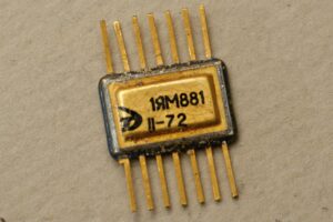
1YaM881 – 1972
The next in a series of static RAM chips was the CMOS K561RU2 (K564RU2), released in 1976. 564 series of chips is a “military” analogue of the 561 series. In these series, there are several dozen microcircuits. The chip has an organization of 256 words by 1 bit.
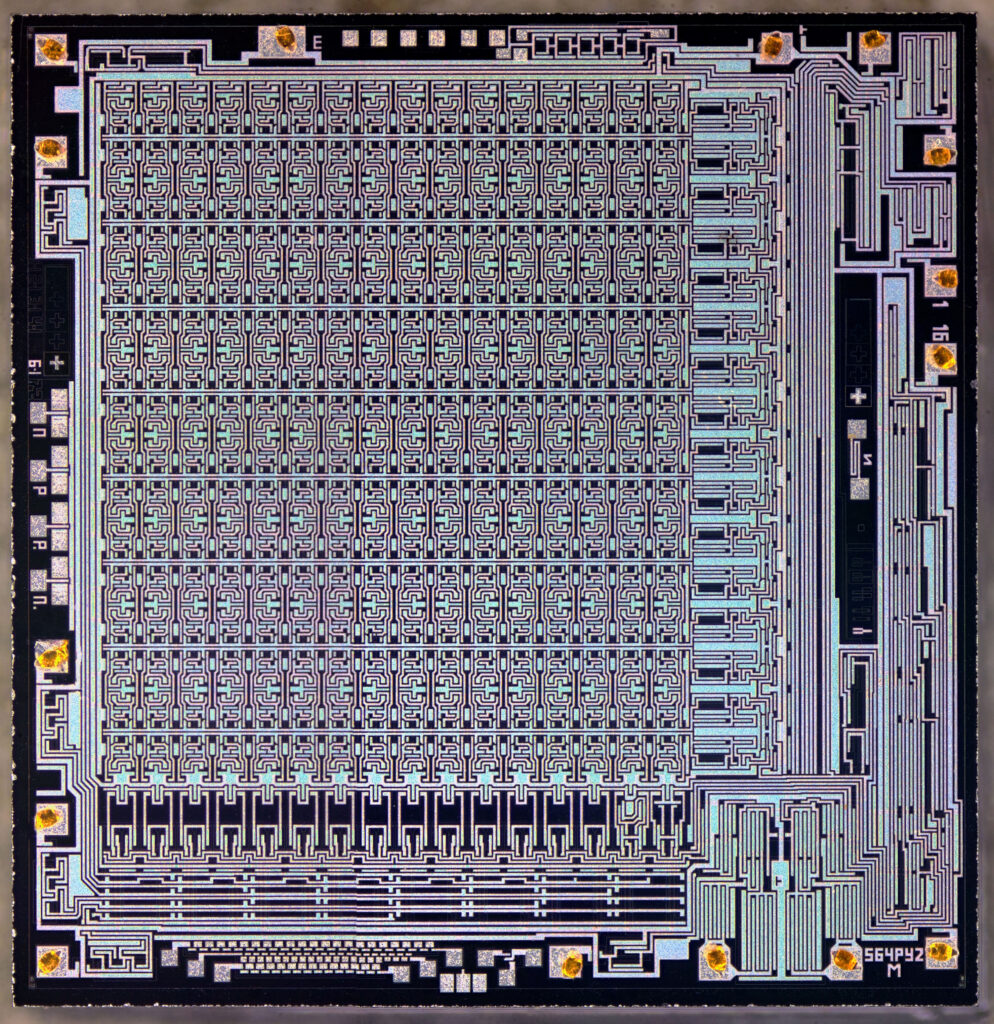
561RU2 die – 16×16 256bit matrix clearly visible – The image is taken from the site https://radiopicture.listbb.
It contains 2067 integral elements. Supply voltage is 3-15 volts. It’s an analogue of CD4061A. It should be noted that in most cases ‘analogue’ means similar to, not an exact copy or exactly compatible. The USSR did make some compatible IC’s, but they mostly made stuff that was similar, but built to their own specifications/needs.
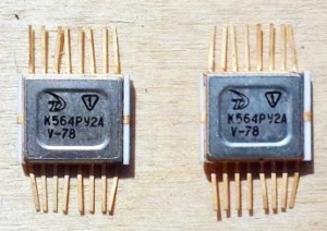 K564RU2A -1978 |
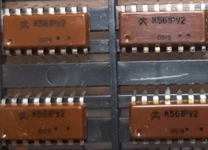 K561RU2 -1979 |
The package of the K561RU2 chip is wider than the standard packages of this series.
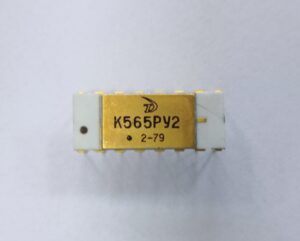
K565RU2 -1979
The K565RU2 static RAM chip was manufactured using NMOS technology. Chip capacity was 1024 bits (1024×1). Contains 7142 integral elements. An analogue of Intel 2102A, developed in 1974. K565RU2 appeared in 1977. It was originally designed to be placed in a ceramic package, but later, in order to reduce the cost of production, the dies began to be packed in plastic packages.
Posted in:
CPU of the Day