August 12th, 2021 ~ by admin

Forgotten Italian CPU – The Genesys B52 MMX

Introduction

On this site you can read about thousands of processors models. And every year it is more and more difficult to write about some new (old) processors, since everything has been known for a long time. But there are also exceptions to the rule which we love to find. In 2021, I learned about one unusual processor, the information about which I want to share with you. The roots of this processor’s history go back to Italy, in the distant year or 1998. This time just falls on the confrontation between Intel and its second generation Pentium and AMD K6-2 and K6-3 processors. The Cyrix MII processors from Cyrix Corporation, IDT WinChip 2s and Rise mP6s were still going strong as well.

But before we talk about the Genesys B52 MMX processor, we should take a closer look at Intel Pentium II processors in general, as the Italian processor primarily owes its appearance to them.

Intel Pentium II

From 1993 to 1997, the Pentium dominated all market segments. Over time, the name of the “Pentium” trademark even grew into a household name (Its all about the Pentiums baby), but with the release of the Pentium II, everything changed. If earlier Intel did not deeply segment the market, there were Pentium Pros for workstations and servers, and for everything else there were various models of Intel Pentium processors, in which, at the end of their domination, Intel added MMX instructions, depriving and thereby putting an end to its server segment. The new slot form factor of the processor, the abandonment of the usual pins and ceramics and further segmentation of the market (using Intel Celeron processors and the new Xeon line) radically changed the further course of development of the history of microprocessors.
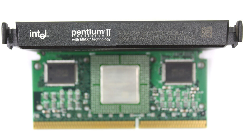
May 7, 1997 saw the light of the first models of Intel Pentium II processors, manufactured on a 350nm process with a core voltage of 2.8 volts. The first models were based on the Klamath core (named after the river by which The CPU Shack is located) core, operating at 233 and 266 MHz. The main differences from the Pentium Pro predecessor it was based on were the L1 cache increased from 16 to 32 Kb, and the presence of a block of SIMD instructions called MMX first introduced on the last P55C processors. Like the Pentium Pro it featured its own L2 cache on the module, but in this case it was 512KB fixed on the same PCB as the processor core, a much cheaper solution then the dual ceramic cavity package of the Pentium Pro.

Before the Pentium II, only the Pentium Pro could boast of its own cache, running at the frequency of the CPU core. But, placing the CPU core and L2 cache on the same substrate was an expensive pleasure even for Intel, and the processors had to be cheaper for better competition, which was getting more and more intense. Intel then made a “wise” decision, as a result of which the Pentium II got a its own L2 cache next to the CPU core This engineering solution significantly reduced the cost of manufacturing processors. BSRAM L2 cache chips were manufactured by Toshiba, SEC and NEC at that time, rather then being made in house by Intel, further easing the cost burdens.

Pentium II Klamath SECC1 PBGA Core 2 x Cache on front 2x + TAG on back

For all models of Pentium II processors, the cache size remained unchanged and equaled 512 KB, while different Pentium Pro models had a cache from 256 to 1024 KB. The L2 cache of the first Pentium II processors consisted of four microcircuits located on both sides of the cartridge processor board and operated at half the core frequency. In addition to the processor core and 4 L2 cache chips, there was also a tag-RAM chip on the cartridge PCB, a total of 6 IC’s.

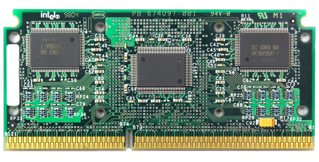
Backside with 2x cache + TAG

The tag-RAM size/configuration determines which range of main memory can be cached. For example, if the L2 cache is 256 KB and the tag RAM is 8 bits wide, then this is enough to cache up to 64 MB of main RAM. However, if you add additional RAM in the process, it will not be cached unless you also expand the tag RAM. On Socket 1-3 486 systems, most motherboards allowed adding and modifying additional L2 cache and tag-RAM chips for this purpose. The Pentium Pro had built-in L2 cache and tags capable of caching up to 4GB of main memory, whereas the first Pentium IIs could cache up to 512MB of RAM.  This was in part to set them apart from the server oriented Pentium II Xeon which had full speed cache capable of caching 4GB (or 64GB with PSE-36),

In January 1998, Intel announced the Pentium II processor, built on a new core, codenamed Deschutes (Another river in Oregon). The processor core was manufactured using the smaller 250nm process, which lowered the operating voltage to 2.0 V, instead of 2.8 V for “Klamath”. The L2 cache of 512 KB still worked at half the core frequency, but it was made in the form of two BSRAM chips located to the side of the processor package. In later modifications of the Pentium II Deschutes core, Intel replaced the tag-RAM chip, thanks to which the processors could cache up to 4 GB of RAM (the 82459AD revision).

The first generation of Intel Celeron processors were based on the “Covington” core were essentially processors on the “Deschutes” core, but without ANY L2 cache. Thanks to this, they had very poor performance, but they overclocked very well, demonstrating the best overclocking figures up to double the nominal clock frequency.

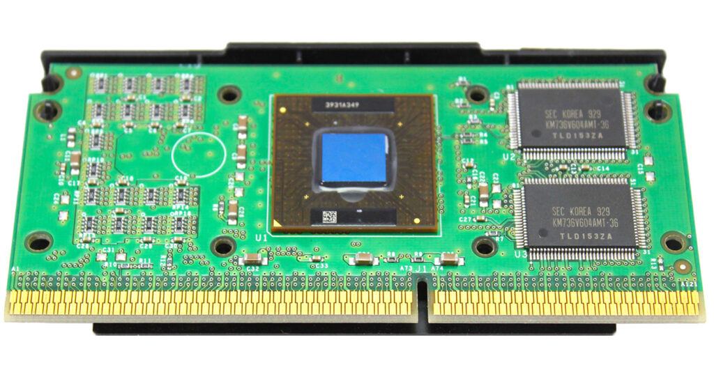
Deschutes core with Organic BGA core and 2x cache chips on front. TAG on back

All overclocking of Pentium II, as a rule, rested on the characteristics of microcircuits used by BSRAM and tag-RAMs. The latter, like the cache, was much disliked voltage rises, and with inept handling, an expensive Pentium II could turn out to be a Celeron “Covington”, if such microcircuits failed.By the way, they warmed up decently on Pentium II processors based on the “Klamath” core so cooling was very important as well. The multiplier in 99% of Pentium II processors was locked (very early production ones were unlocked and Engineering Samples of course), so overclocking was performed by raising the FSB frequency, this being dependent always on the cache and TAG chips installed in that particular processor.


A simple example. In Costa Rica, where Intel has an advanced advanced processor assembly/test factory, which simultaneously assembled high-frequency models with 450 and 300 megahertz. The cartridge and core for these processors are identical (and the multiplier was the same 4.5x as well 66×4.5 for the 300 and 100×4.5 for the 450). The difference was only in the installed cache memory with different speed rating in nanoseconds. Sometimes on the assembly line there was only a fast cache memory capable of operating at a frequency of 225 MHz, intended for models of processors with 450 MHz. In this case, it was also installed on the model with a frequency of 300 MHz, as a result of which they overclocked perfectly.
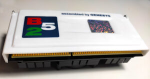
Genesys B52 MMX CPU

The history of the Italian processor began in the city of Monopoli, in the province of Bari in Italy. In 1998, Italian Marcello Console founded Genesys, which initially employed 10 people. The main idea of the Genesys business was the production of modified Intel Pentium II processors based on the “Deschutes” core, at a much lower price than the Pentium II ones of similar clock speed. Plus a warranty period extended to 3 years and productivity increased by 5% or more. It turns out to be a solid Attraction of Generosity!

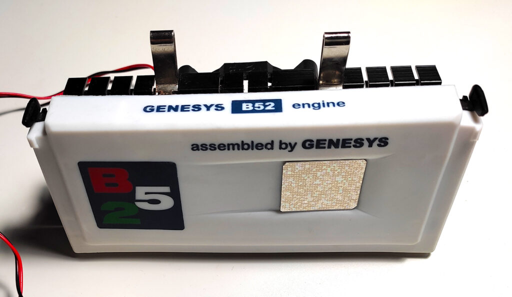
Genesys had registered its own domain www.b52mmx.com and is getting ready to implement their processors in ready-made system units. Unfortunately, nothing is known about the manufacturing process, it remains a mystery to this day. There is not so much information on these processors, but let’s try to figure out what these processors were.

Read More »

March 20th, 2020 ~ by admin

The Intel N60066: Unwrapping a Mystery

Fischer & Porter 53MC5 – The beginning of the Mystery

One day last summer, I was browsing the deep dark corners for processors, a fun, yet dangerous activity.  I happened upon a lot of PCBs from some older industrial automation equipment.  No real information was provided (those buying these boards clearly would already know what they needed).  They did however have a RTC, an EPROM a 16MHz crystal, and a large 84-pin PLCC.  That PLCC was marked as an Intel N60066.  Seeing such a large chip, surrounded by such components almost always means its some sort of processor or microcontroller.  The problem is, there is no known Intel 60066 part.  The chips were all made in the late 80’s and early 90’s and had  1980 and 1985 copyrights.  A 1980 copyright typically screams MCS-51, as that was when it was introduced and nearly all such chips bear an Intel 1980 mark.

Intel N60066

The boards themselves were dated from 1990 all the way to the early 2000’s (I bought a lot of them, another problem I have).  Some had the part number 53MC5 and the logo of Fischer & Porter.  Fischer & Porter has existed since the 1930’s and was a leader in instrumentation.  They were bought by Elsag Bailey Process Automation (EBPA) in 1994 which itself was swallowed up by ABB in 1999.  The boards design was largely unchanged through all of these transitions. Searching for documentation on the 53MC5 part number (its a Loop Controller) didn’t yield details on what the N60066 was unfortunately.  The only thing left to do was to set it on fire…

Unfortunately this is the only way I currently have for opening plastic IC’s (I need to get some DMSO to try apparently).  After some careful work with the torch and some rough cleaning of the resulting die it was readily apparent that this was an MCU of some sort.  The die itself was marked… 1989 60066.  This wasn’t a custom marked standard product, this was a custom product by Intel for this application, a very surprising thing indeed.  Unlike other companies such as Motorola, Intel was not well known for custom designs/ASICs.  This wasn’t their market or business plan.  Intel made products to suit the needs they saw, if that worked for the end user, great, if not, perhaps you could look elsewhere.  They would gladly modify specs/testing of EXISTING parts, such as wider voltage ranges, or different timings, but a complete custom product? Nope, go talk to an ASIC design house.  Its likely Fischer & Porter ordered enough of these to make it worth Intel’s effort.

Knowing this was an MCU and suspecting a MCS-51 further searching revealed the answer, and it came from the most unusual of places.  In 2009 the US NRC (Nuclear Regulatory Commission) determined there was no adequate Probabilistic Risk Assessment (PRA) for Digital systems in their agency, so set about determining how best to calculate risk of digitally controlled systems.  They analyzed a system used to control feedwater in nuclear reactors.  These are critical systems responsible for making sure the reactor is kept with the right amount of cooling water at the right time, failure of course is not an option.  The 53MC5 is what is used for controlling the valves.  In this document we find this nugget:

The controller is an 8051 processor on board an application-specific integrated circuit (ASIC) chip that performs a variety of functions.

Well that certainly helps, it is indeed a custom ASIC based on an 8051.  The report also provided a diagram showing the ASIC system.  This is an 8051 core with RAM/ROM (normal) as well as a Watchdog timer, a PAL, I/O Buffers, and Address Logic.

I sent a couple of these chips to my friend Antoine in France for a proper die shot, which he is quite amazing at.

Intel N60066 die – 8051 core on the left. Die shot by Antoine Bercovici

The 8051 core is on the left of the die, with its RAM/ROM.  A very large PLA occupies the bottom right side of the day.  In the upper right is presumably the external watchdog timer for the ASIC.  The lines crossing the die mostly vertically are a top metal layer used for connecting all the various sections.

The hunt for a new CPU/MCU is part of the thrill of collecting.  The satisfaction of finding out what a mystery chip is can be worth many hours of dead ends in researching it.  Its not common to have to go to the NRC to find the answer though.

Tags:
,

Posted in:
CPU of the Day

October 1st, 2019 ~ by admin

The Story of the IBM Pentium 4 64-bit CPU

Introduction

This time we will talk about one unique Intel processor, which did not appear on the retail market and whose reviews you will not find on the Internet. This processor was produced purely by special order for one well-known manufacturer of computer equipment. Also in the framework of this article I will try to assemble one of the most powerful retro-systems with this processor.

From the title of the article, I think many people understand that we will talk about the Socket 478 Intel processor

Most people are familiar with the Socket 478 that replaced Socket 370 at the end of 2001 (we omit Socket 423 due to its short lifespan of less then a year) and allowed the use of single-core, and then with Hyper Threading technology “pseudo-dual” processors that can perform two tasks in parallel. All production Intel processors within Socket 478 were 32-bit, even a couple of representatives from the Pentium Extreme Edition server segment on the «Gallatin» core. But as always there are exceptions. And this exception, or to be more precise, two exceptions, were two models of Pentium 4 processors with the Prescott core, which had 64-bit instructions (EM64T) at their disposal.

Intel Pentium 4 SL7QB 3.2GHz: 64-bits on S478

This pair of processors were commissioned by IBM for its eServer xSeries servers. These processors never hit the retail market and their circulation was not very large, so finding them now is very problematic. It is interesting that the fact that if you want and naturally have the right amount of money, or a large enough order, you can count on a special order of the processor that is needed for the specific needs, with characteristics that will be unique and will not be repeated in standard production products. And it should be noted that not a few such processors have been released, in fact, in the 70’s and early 80’s this was the very purpose of the now ubiquitous ‘sspec.’ Chips with an Sspec (Specification #) were chips that had some specification DIFFERENT from the standard part/datasheet.  A chip WITHOUT a sspec was a standard product.  By the late 1980’s all chips began to receive sspecs as a means of tracking things like revisions, steppings, etc.  I will talk about some a little later.

hat’s how the processor looks through the eyes of the CPU-Z utility. In the “Instructions” field after SSE3, the EM64T proudly shows off! Link to popular CPU-Z Validation.

Special processors made for IBM belonged to the Prescott core and were based on E0 stepping with support for 64-bit instructions, which is not typical for Socket 478! The first 64-bit CPUs for “everyone” appeared only with the arrival of the next LGA775 socket, and even then it wasn’t right away; some Pentium 4 models in LGA775 version were 32-bit. I specifically pointed out that the Pentium 4 Socket 478 model with EM64T support belonged to the E0-stepping, although later the more advanced stepping G1 was released, which did not have such innovations. The first model worked at a frequency of 3.2 GHz and had a SPEC code – SL7QB, the second was slightly faster with a frequency of 3.4 GHz and the SPEC code – SL7Q8.

For the rest, these were the usual «Prescott». But the presence of 64-bit instructions made these processors unique, capable of working with 64-bit operating systems and the same applications, allowing them to do what their 32-bit comrades simply could not do.

Read More »

August 15th, 2018 ~ by admin

CPU of the Day: The 61 Knights of the Intel Xeon Phi

Xeon Phi – Knights Corner – Engineering Sample

In June of 2013, 20 years after the release of the Intel Pentium Processor, Intel released a new processor, technically a co-processor that Intel referred to as a MIC (Many Integrated Core).  It was branded as a Xeon, specifically the Xeon Phi 7000 series but at its core, it was nothing like a Xeon of 2013.  Code named Knights Corner, it built on the Knights Ferry.  Knights Ferry used many Larrabee GPGPU cores and was not designed as a commercial product.  Knights Corner , however, was, and to do so, Intel stuck with an architecture that customers were very familiar with, x86.  The Knights Corner integrated 61 Pentium P54CS cores onto a single chip.  The original Pentium P54CS was made on a 0.35u process and topped out at 200MHz.  They included 16K of L1 cache on die, and typically 256-512K of L2 Cache off chip.  The implementation of the Pentium on the Phi gets a bit of an upgrade.  The cores are made on a 22nm process (16 times smaller) and clocked at up to 1.2GHz.  L1 cache has been increased to 64K per core (32K Instruction  32K Data).  L2 cache remains at 512K

Knights Corner Die. – 62 Cores – 8 GDDR5 Memory Controllers

per core, but at 22nm, integrating all 30.5MB of cache on the same die becomes relatively easy.  The biggest change to the cores is adding support for 64 bit instructions, as well as adding a new execution unit called the VPU. This VPU (Vector Processing Unit) has its own 512-bit wide SIMD instruction set, integer support, Fused Multiply/Add, and other advanced features that are more commonly found in GPU’s. The VPU is the result of Intel’s work with Larrabee, the precursor to Knights Corner.  Interestingly MMX/SSE are not supported by the cores natively, this is handled in software (using virtualization) and leveraging the VPU included with the 61x Pentium Cores.  With the VPU, each core has 4 execution units (VPU, FXU, and 2 x Integer units). This allows the cores to support 4-way multi-threading; in practice, 2 threads are most common as 2 execution units are usually tied up calculating memory addresses.

Knights Corner Sample – This is a 1.09GHz part while production versions were bumped to 1.1GHz – Elpida 2Gbit GDDR5 RAM chips surround the core.

For some reason Intel was very vague about information on die sizes/transistor count on the Phi.  Many sources claim 350mm2 die with 5 Billion transistors.  Taking apart a Phi shows that the die is actually much larger.  In fact the Xeon Phi die is 705mm2 and has 5.1 Billion transistors.  A 22nm Haswell Xeon with 18 cores has a die area of 622mm2 containing 5.6 Billion transistors. This means the Xeon Phi die wasn’t the most efficient is its use of space, likely due to the amount of room needed for the very large rings used to connect all the cores.  Looking at the die you can also see a lot of unused space.   There are actually 62 cores per die (with only 61 used max.)  This means 31MB of L2 cache which at 6 transistors per cell (bit) accounts for 1.5 Billion of the transistors.  L1 Cache is 64K per core so another 190 Million transistors there.  That leaves the bulk of the die for the cores, memory controllers, and the 3 interprocessor communication rings that handle communication between cores, MC’s (8 GDDR5 Memory Controllers per die), and the outside world.

Each Xeon Phi board includes the processor, as well as 6-16GB of GDDR5 Memory (8GB on the Engineering Sample here).  Memory is handled by 32 Elpida EDW2032BBBG-6 2Gbit GDDR5 6 Gbps chips. This gives the card is 352 Gbps memory bandwidth and 1 TFLOPS of computing performance.  All in a PCI-E car that dissipates around 300W.   Card/System management is provided by a NXP LPC2365FBD100 72MHz ARM7TDMI processor.

Knights Corner Xeon Phi with cooler removed. 16x 2Gbit GDDR5 (+16 on the back)

In January of 2013 the Texas Advanced Computing Center in Austin, TX announced the Stampede Supercomputer, the first large scale deployment of Xeon Phi Processors.  It used 6880 of them in its 6400 compute nodes and could hit nearly 10PFLOPS of performance. In June of 2013 the Chinese supercomputer Tianhe-2 became the fastest supercomputer in the world, a title it held until the end of 2015.  It was powered by 32,000 Intel Xeon E5-2692 2.2GHz 12C Ivy Bridge processors and a massive 48,000 Xeon Phi co-processors resulting in over 33PFLOPs.

Tianhe 2 Super Computer with 48,000 Knights Corner Processors.

Intel made a successor to Knights Corner, known as Knights Landing, that was based on the Atom core, but then began to wind down the project.   Avinash Sodani, chief architect of the Knights Landing chip took a job at Cavium Networks (who make multicore MIPS networking processors), and Intel then hired Raja Koduri, the chief architect of AMD’s GPU processors.  Intel’s future seems to be one based on Xeon, and GPU’s.

Like the Knights of old, the the Xeon Phi has been passed up by other technologies, certainly still useful, but destined to the halls of museums and history books.  It came, and it conquered the Top500 Supercomputer list, and then quietly fades away.  On July 27th Intel quietly announced the discontinuation of the Xeon Phi line, with last orders accepted the end of this August (2018).


July 23rd, 2018 ~ by admin

A Sampling of Sample Processors

AMD K6-2 Marketing Sample

During the development of most any given processor many chips are produced before it is released for commercial use.  These pre-production chips serve a wide variety of purposes in the design and debugging of the processor to ensure that the final CPU work well, sells well, and is compatible with all the vendors parts (motherboards, cooling solutions, power supplies, etc).  These chips are generally referred to as samples, and there is several types of them.  We’ll use Intel/AMD as the main examples but most all processor companies work in similar ways.

When a processor design is first being developed, the package for it is also often being developed as well, what will the new processors silicon die reside in?  How many pins? How will it dissipate heat?  This type of testing is often handled with Mechanical Samples.  Mechanical Samples are exactly as they sound, they test the mechanical aspects of the processor, the physical fit of it.  THese are often sent to board/socket manufacturers to ensure the processor will fit in sockets/boards, and with the automated equipment used to build systems.  Cooling solution companies may also receive these to test how a heatsink fits on the CPU. Mechanical samples may not contain a die at all, or may be chips that were tested as bad, or simply just untested chips (Intel used a lot of untested Mechanical Samples in their educational kits).

Thermal Sample for the LGA2011 Sandy Bridge Xeon

The next samples typically made are Electrical/Thermal Samples.  These again do not have an actually processor die in them, but electrically do work.  Electrical/Thermal samples are used to test the power draw and heat dissipation of a processor.  They often use a daisy chain transistor design, which serves to draw/dissipate power.  If a processor is expected to dissipate 135W of heat, a Thermal sample can be made to draw/dissipate exactly that.  These can test the the power supplies on motherboards, as well as the heat dissipation abilities of cooling solutions.  Some Thermal Samples have a temperature sensor added directly to the package to help see what temps they achieve.  Electrical Samples and Thermal Samples could also be used as purely Mechanical Samples too, and this is sometimes seen marked on the sample.

The first samples made that actually contain a functioning processor die are Engineering Samples.  Engineering Samples (also known as ES) are the most well known samples.  Overclockers often like to find ES CPUs as they will often allow for easier overclocking due to some not having locked in speed (multiplier locked).  Engineering Sample CPUs themselves come in several types as well.  Usually the first run is known as ES1, these can be thought of as an ‘Alpha’ version.  They are very likely to be buggy, and rarely run at the same speed as a production chip would.  These exist to test the overall processor design, or some subset of it.  Some are made to test just one part of the CPU, for example , the memory controller, or the cache.  Later versions of

Motorola PowerPC 8260 Engineering Sample (note the PPC prefix)

Engineering Samples are often called ‘ES2.’ These processors are getting closer to final production and are a lot less buggy, these would be considered ‘Beta’ Samples.  Most of the time these are quite usable chips, and often are very similar in clock speed/features to a production processor.   Intel denoted these chips with a Q-spec (such as QBGC) rather then production processor having an S-spec (such as SL5G8).  AMD typically uses part numbers starting with ‘1’ for ES1 CPUs and ‘2’ for ES2 CPUs. (such as Opterons 1S160805L4BGC or 2S16….).  Other companies have similar methodologies.  Motorola (Freescale) used the PPC prefix for most ES CPUs and Texas Instruments uses ‘TMP’ (not to be confused with Toshiba who also uses the TMP pre-fix, but for processors in general). Once a company is fairly confident a design is ready for release one final version is made.

These are known as Qualification Samples (QS).  QS processors almost always have a one to one equivalence with a production part, since that is their purpose, to make sure the design is ready for release.  These processors are by far the most widely made chips, as they are shipped by

Alchemy Au1000 MIPS Processor – Qualification Sample

the thousands to vendors, system builders/integrations, and even the media outlets for review.  The hope is that nothing major wrong is found with them, and that any bugs that are found can be dealt with in software or firmware, not requiring an entire silicon fix.  Intel continues to use Q-specs for these as well, leading to some confusion with the previously mentioned ES CPU’s.  AMD usually uses part numbers beginning with ‘Z’ for QS CPU’s and like Intel, does not offer these CPU’s for sale to the general public, they are either given to vendors, or sold exclusively to them for testing.   Motorola uses XC, or XPC for these, and unlike AMD/Intel, mass produces these and sells them, often for years, before they decide that a part/design is truly fully qualified/characterized (in which case the prefixe is changed to MC. or MPC).  Texas Instruments uses the ‘TMX” prefix for their Qual. Samples. and tended to make/sell them like Motorola did with theirs, changing the prefix to TMS for fully qualified production parts.

Read More »

Posted in:
CPU of the Day

July 3rd, 2018 ~ by admin

CPU of the Day: The Intel Everest Series

Mt. Everest – Tallest on Earth

Mt. Everest is the tallest mountain here on Earth, the pinnacle of climbing challenges.  There is no going higher then Mt. Everest.  At Intel the pseudo-unofficial codename for the absolute fastest speed bin of a particular processor is…Everest.  Everest processors are the fastest an architecture will so reliably.  Sometimes these processors end up an normal products, available for consumers to purchase.  The first good example of this is the Core 2 Extreme QX9775 Yorkfield core (Core Architecture).  They were a quad-core processor running at 3.2GHz, fast but not mind blazingly so.  The Xeon equivalent was the X5492 (Harpertown) 4-core at 3.4GHz.

Xeon X5698 – Westmere – 4.4GHz – Mid 2010

The next well know Everest was a chip based on the Westmere (shrink of Nehalem) architecture.  The Westmere Everest became known as the Xeon X5698, and was available for OEMs only, in fact it was a special order processor made with one particular type of client in mind. These were to be used for High Frequency Stock traders, and other such high speed transactional processing, where the ability to complete trades as fast, and reliability as possible is the entire nature of the business.  This means that single thread performance is far more important then having multiple core, and as such, the X5698 uses a 6-core die with only 2 cores active, but retaining access to the entire 12MB of L3 cache.  Clock speed was fixed at 4.4GHz, the cores did not reduce frequency as processing demands changed, as this would introduce uncertainty in how fast it would complete a given task. Doing task ‘X’ should take a predictable amount of time and not depend on what speed the processor chose to run at.  The next fastest Westmere processor was the X5690, which was a 6-core (all cores enabled) running at 3.46GHz (the same chip essentially as the Core i7 990X).  The X5698 was nearly 1GHz faster.  The X5690 cost around $1800, where as the X5698 cost around $20,000 EACH (based on costs OEMs charged to add a 2nd one so they may have marked it up some).  The impressive thing is that these chips would go faster.  Intel sampled 4.66GHz versions and Supermicro built systems using X5698’s overclocked to 4.8GHz.  All this back in 2011.

4.4GHz Jaketown (Sandy Bridge) Everest Sample 2010-2011

Intel’s next architecture was known as Sandy Bridge.  Sandy Bridge topped at at 3.5GHz (6-cores) for the Core i7 Extreme 3970X and 3.6GHz for the 4-core i7-3820 and similar Xeon E5-1620.  Intel demo’d an air cooled Sandy Bridge running on stage for a presentation at 4.9GHz, so the core certainly had some room to spare.  There is no documentation (that I could find) that Intel actually released anything faster then 3.6GHz, at least that I could find, but evidence suggests that they at least were thinking about it.  The picture is a Sandy Bridge Xeon in LGA2011 marked JKT EVEREST SS 4.4GHZ INTERNAL USE ONLY. JKT is short for Jaketown, Intel’s codename for the 32nm Xeon E5-2600 series.  That gives a very good idea what this processor was to be.  SS is likely to be a Single Socket (as often at those speeds getting dual systems working can be tricky).  Sandy was certainly capable of hitting 4.4GHz, with 4-core, and even air cooling, so perhaps these were samples for a limited OEM run, much like the previous Westmere X5698 processors.

Read More »

March 24th, 2018 ~ by admin

Making MultiCore: A Slice of Sandy

Intel Sandy Bridge-EP 8-core dies with 6 cores enabled. Note the TOP and BOTTOM markings (click image for large version)

Recently a pair of interesting Intel Engineering Samples came to The CPU Shack.  They are in a LGA2011 package and dated week 33 of 2010.  The part number is CM8062103008562 which makes them some rather early Sandy Bridge-EP samples.  The original Sandy Bridge was demo’d in 2009 and released in early 2011.  So Intel was making the next version, even before the original made it to market.  The ‘EP’ was finally released in late 2011, over a year after these samples were made.  Sandy Bridge-EP brought some enhancements to the architecture, including support for 8-core processors (doubling the original 4).  The layout was also rather different, with the cores and peripherals laid out such that a bi-direction communications ring could handle all inter-chip communication.

Sandy Bridge-EP 8-core die layout. Note the ring around the inside that provides communications between the peripherals on the top and bottom, and the 8-cores. (image originally from pc.watch.impress.co.jp)

Sandy Bridge EP supports 2, 4, 6 and 8 cores but Intel only produced two die versions, one with 4 cores, and one with 8 cores.  A die with 4 cores could be made to work as a dual core or quad, and an 8-core die could conceivably be used to handle any of the core counts.  This greatly simplifies manufacturing.  The less physical versions of a wafer you are making, the better optimized the process can be made.  If a bug or errata is found only 2 mask-sets need updated, rather then one for every core count/cache combination.  This however presents an interesting question..What happens when you disable cores?

That is the purpose of the above samples, testing the effects of disabling a pair of cores on an 8-core die.  Both of the samples are a 6-core processor, but with 2 different cores disabled in each.  One has the ‘TOP’ six cores active, and the other the ‘BOTTOM’ six cores are active.  This may seem redundant but here the physical position of the cores really matters.  With 2 cores disabled this changes the timing in the ring bus around the die, and this may effect performance, so had to be tested.  Timing may have been changed slightly to account for the differences, and it may have been found that disabling 2 on the bottom resulted in different timings then disabling the 2 on the top.

Ideally Intel wants to have the ability to disable ANY combination of cores/cache on the die.  If a core or cache segment is defective, it should not result in the entire die being wasted, so a lot of testing was done to determine how to make the design as adaptable as possible.  Its rare we get to see a part from this testng, but we all get to enjoy its results.

March 15th, 2018 ~ by admin

CPU of the Day: Intel Jayhawk – The Bird that Never Was

Intel Jayhawk Thermal Sample – 80548KZ000000 QBGC TV ES – Made in April 2004 Just 3 weeks before it was canceled

Perhaps fittingly the Jayhawk is not a bird, but rather a term used for guerilla fighters in Kansas during the American Civil War.   It is also the name of a small town in California 150 miles Northeast of Intel’s headquarters in Santa Clara.  It was also the chosen code name for a Processor Intel was working on back in 2003.  In 2003 Intel was working on the Pentium 4 Prescott processor, to be released in 2004 and its Xeon sibling, the Nocona (and related Irwindale),  The Prescott was a 31 stage design made on a 90nm process.  There was hopes it would hit 4+ GHz but in production it never did, though overclockers, with the help of LN2 cooling were able to achieve around 8GHz.  Increasing the length of the pipeline helps allow higher clock speeds, the Northwood core had a 20-stage pipeline so the Prescott was a rather big change.  There is a cost of lengthening the pipe, processors don’t always execute instructions in order, often guessing what will come next to speed up execution.  This is called speculative execution, processors also guess what data is to be needed next, and stick it in cache.  If either of these ‘guesses’ is wrong, the processor needs to flush the pipeline and start over, at a comparatively massive hit in performance.  This is what performance doesn’t always scale very linearly with clock speed.

Intel figured that this wouldn’t be an issue and so the Prescotts successor was to have a 40-50 stage pipeline.   THe hopes were for 5GHz at 90nm and 10GHz at 65nm. The desktop version was known as Tejas, and the server version, Jayhawk.  Initially these were to be made on the 90nm process, same as Prescott, before being transitioned to a 65nm process.  It increased the L1 cache to 24k (some sources say 32k) from the Prescotts 16k.  The Instruction trace cache was still 16k micro-ops, though this could have been increased.  L2 cache would have been 1MB at introduction and 2MB once the processor moved to a 65nm process.  Eight new instructions were to be added called ‘Tejas New Instructions’ or TNI, these later would become part of the SSSE3 instructions released with the Core 2 processor.  It also would bring ‘Azalia’ Intel’s High definition audio codec, DDR2 support, a 1066MHz bus, and PCI-Express support.  It turns out there was a problem….

Read More »

November 24th, 2017 ~ by admin

New Test Board Available for Sale: Intel 3002 Bit-Slice Processor

3002 Test Board

We have released a simple (its our least expensive board yet) Test Board for the Intel 3002 Bit-Slice Processor.  The Intel 3000 bit-slice processor family was introduced in 1973 and were made on a  Schottky Bipolar process. The 3002 series was also second sourced by Signetics, Siemens, and Intersil, and clones were made by the USSR and Tesla  (Czech).  The 3002 CPE is a 2-bit ALU and register file that can perform logical and arithmetic operations, left/right shifting and bit/zero value testing. The 3002 also includes 11 registers (R0-R9, T), an accumulator and a Memory Address Register (MAR). The 3002 CPE elements execute micro instructions generated by the 3001 Microprogram Controller Unit (MCU) based on micro code stored in PROM.
Its only $69.95 (including FREE shipping worldwide)

Order it on the 3002 test Board page.

In other related news, we are also developing a test board for some other BSP. Hopefully we’ll have a single board (with expansions) that can handle AMD 2901/03/203 and MMI 6701 processors

Tags:
, ,

Posted in:
Products

August 17th, 2017 ~ by admin

Intel Broadwell Broadens its Horizons…In Space

SpaceX CRS-12 – Carrying 116lbs of High performance Broadwell computers (image: SpaceX)

Monday’s launch of a SpaceX Falcon 9 rocket carrying a Dragon spacecraft to the space station carried what will be the most powerful computer in orbit.  In a joint project with HPE (HP Enterprise) NASA wants to test how high end computers, with off the shelf parts and construction perform in low Earth orbit.  The computer that will be soon installed is an HP Apollo 40 series (exact model is unclear, probably PC40/SX40).  It consists of 2 1U dual socket systems, running Intel Xeon E5-26xx V4 (Broadwell-EP 14nm) processors and supporting infiniband.  The only modification done was to use liquid cooling vs air cooling as the EXPRESS racks on the ISS are not set up to handle the heat load the computer generates.  The computers run on a standard 110VAC supply, provided by a NASA supplied inverter, which takes the 48VDC power generated by ISS’s solar arrays and converts it to the 110VAC needed by the Apollo computer.

The Broadwell processors are made on a 14nm process, and are some of the latest made by Intel (NASA froze the design in March so they were the fastest available to HPE at that time).  Performance will be just over 1Teraflop, a great increase over the main computers that actually RUN the ISS, which are Intel 80386SX based.  The astronauts themselves use laptops of various pedigrees, mainly Lenovo Core 2 Duo based A61Ps (these are being replaced by HP Zbook 15s powered by Intel 7th Gen Core i5 and i7 processors) , so the Apollo is a great leap up from them as well.

Mockup of HPE Apollo Computers for EXPRESS rack integrations. 2 computers with water cooling system between them.

To test the Apollo, NASA will run an identical system on the ground, performing the same tasks, and compare the outputs.  They want to see how the computers handle the environment in space, with various loads and electrical conditions.  One computer (both on the ground and on the ISS) will be run at maximum performance for the entirety of the experiment, while the other will have its computing/electrical load dynamically varied.

Radiation is usually one of the biggest concerns for space based computers, but on the ISS, radiation levels are not particularly high.  Daily doses experienced by the crewmembers are in the 10-50 millirad range. There are of course periods of higher radiation, either from where the ISS is in orbit, or from space weather.  The water cooling will further shield parts of the computer from radiation (water being a great radiation shield).  The Broadwell-EP processors have around 7.2 billion transistors, increasing the

10-core Broadwell die. Made on 14nm process.

chance that even a small amount of radiation may have an effect.  By running one set of computers at maximum performance, NASA can see these effects quickly.  Does the performance decrease? Does the power draw start spiking? Or is data being lost in the Infiniband networking PCIe card?

Currently experiment data has to be transferred to the ground in raw unprocessed format, as nothing on the ISS can handle the computing need to process it.  If the high performance computing experiment is successful, it can give the astronauts the ability to do processing and analysis of experimental data in orbit,. and transfer only the results to the ground, saving precious bandwidth, and allowing for experiments to be modified, changed, or created in orbit based on the ongoing results.


More Information: 

NASA: HPC COTS Experiment

HPE: The space station gets a new supercomputer

Tags:
,

Posted in:
Processor News