
CPU of the Day: Intel Jayhawk – The Bird that Never Was
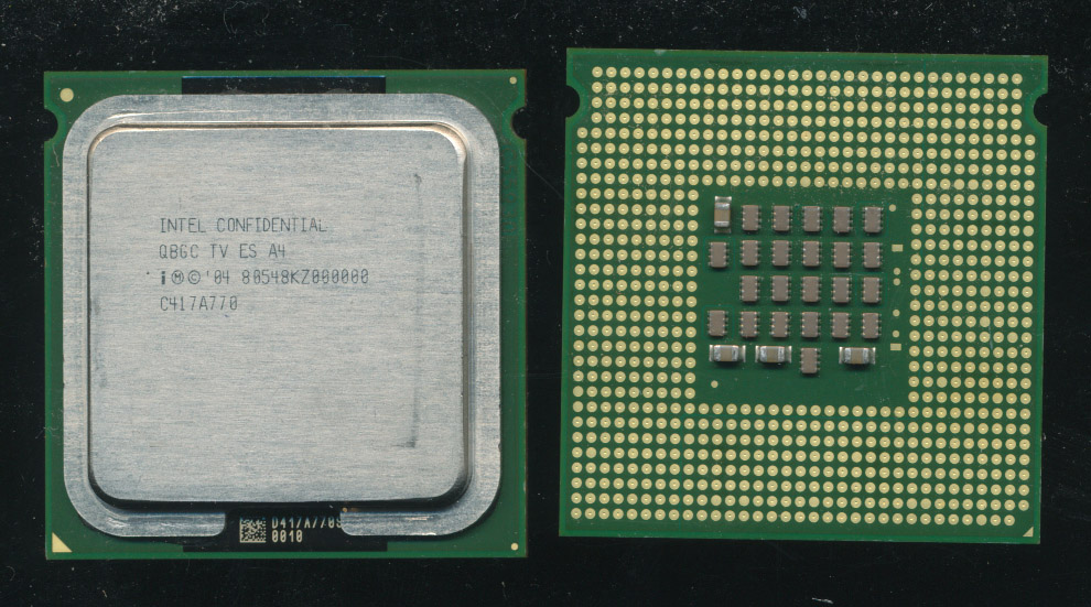
Intel Jayhawk Thermal Sample – 80548KZ000000 QBGC TV ES – Made in April 2004 Just 3 weeks before it was canceled
Perhaps fittingly the Jayhawk is not a bird, but rather a term used for guerilla fighters in Kansas during the American Civil War. It is also the name of a small town in California 150 miles Northeast of Intel’s headquarters in Santa Clara. It was also the chosen code name for a Processor Intel was working on back in 2003. In 2003 Intel was working on the Pentium 4 Prescott processor, to be released in 2004 and its Xeon sibling, the Nocona (and related Irwindale), The Prescott was a 31 stage design made on a 90nm process. There was hopes it would hit 4+ GHz but in production it never did, though overclockers, with the help of LN2 cooling were able to achieve around 8GHz. Increasing the length of the pipeline helps allow higher clock speeds, the Northwood core had a 20-stage pipeline so the Prescott was a rather big change. There is a cost of lengthening the pipe, processors don’t always execute instructions in order, often guessing what will come next to speed up execution. This is called speculative execution, processors also guess what data is to be needed next, and stick it in cache. If either of these ‘guesses’ is wrong, the processor needs to flush the pipeline and start over, at a comparatively massive hit in performance. This is what performance doesn’t always scale very linearly with clock speed.
Intel figured that this wouldn’t be an issue and so the Prescotts successor was to have a 40-50 stage pipeline. THe hopes were for 5GHz at 90nm and 10GHz at 65nm. The desktop version was known as Tejas, and the server version, Jayhawk. Initially these were to be made on the 90nm process, same as Prescott, before being transitioned to a 65nm process. It increased the L1 cache to 24k (some sources say 32k) from the Prescotts 16k. The Instruction trace cache was still 16k micro-ops, though this could have been increased. L2 cache would have been 1MB at introduction and 2MB once the processor moved to a 65nm process. Eight new instructions were to be added called ‘Tejas New Instructions’ or TNI, these later would become part of the SSSE3 instructions released with the Core 2 processor. It also would bring ‘Azalia’ Intel’s High definition audio codec, DDR2 support, a 1066MHz bus, and PCI-Express support. It turns out there was a problem….
Posted in:
CPU of the Day