The Forgotten Ones: HP Nanoprocessor
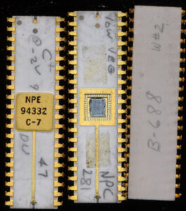
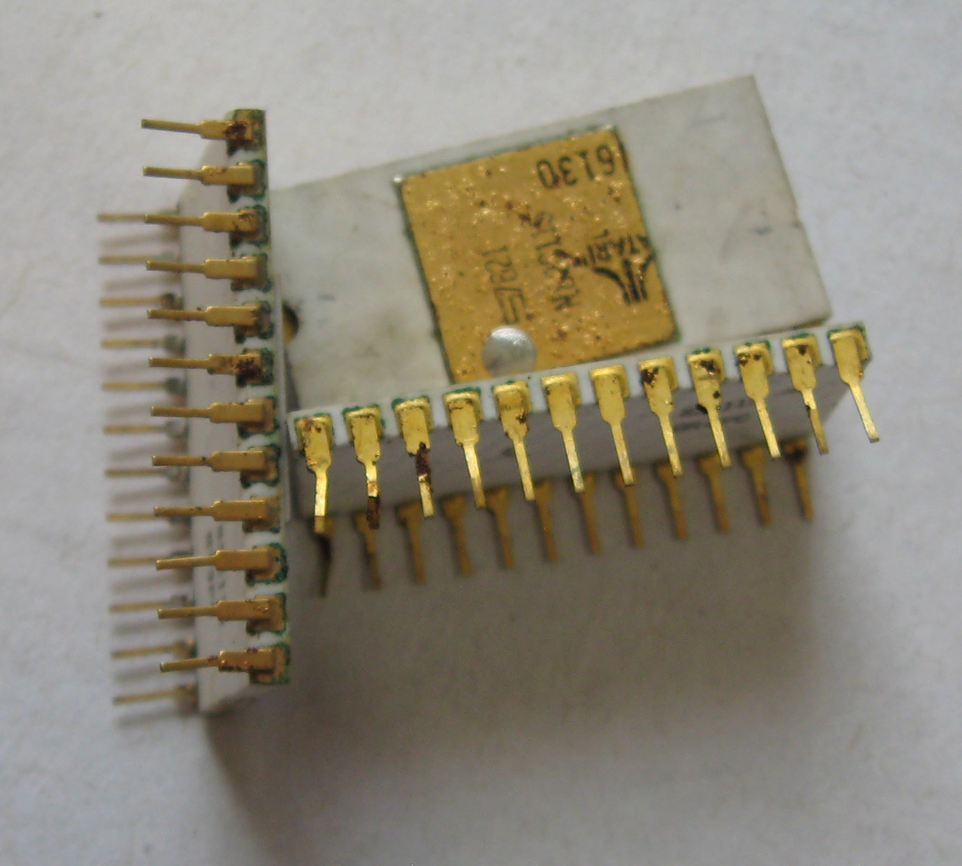
Original Nanoprocessor prototypes from 1974-75. Note hand written wafer number, open die cover and early part number (94332)
Back in the 1970’s the Loveland Instrument Division (LID) of HP in Colorado, USA was the forefront of much of HP’s computing innovation. HP was a leader, and often THE leader in computerized instrumentation in the early 1970’s. From things like calculators, to O-scopes to desktop computers like the 9825 and 9845 series. HP made their own processors for most all of these products. The early computers were based on the 16-bit Hybrid processor we talked about before. At around the same time, in 1974, the HP LID realized they needed another processor, a control oriented processor that was programmable, and could be used to control the various hardware systems they were building. This didn’t need to be a beast like the 16-bit Hybrids, but something simpler, inexpensive, and very fast, it would interface and control things like HPIB cards, printers, and the like. The task of designing such a processor fell to Larry Bower.
The result was a Control Oriented Processor called the HP nanoprocessor. Internally it was given the identifier 94332 (or 9-4332), not the most elegant name, but its what was on the original prototypes and die. The goal was to use HP’s original 7-micron NMOS process (rather then the new 5-micron NMOS-II process) to help save costs and get it into production quickly.
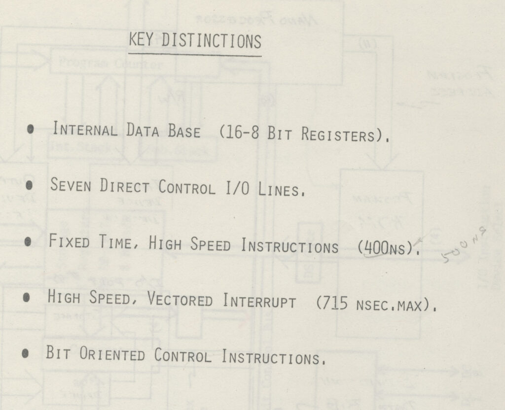
Nanoprocessor Features – Note the speed has been ‘adjusted’
The original design goal was a 5MHz clock rate and instructions that would execute in 2 cycles (400ns). The early datasheets have this crossed out and replaced with 4MHz and 500ns, yields at 5MHz must not have been high enough, and 4MHz was plenty.
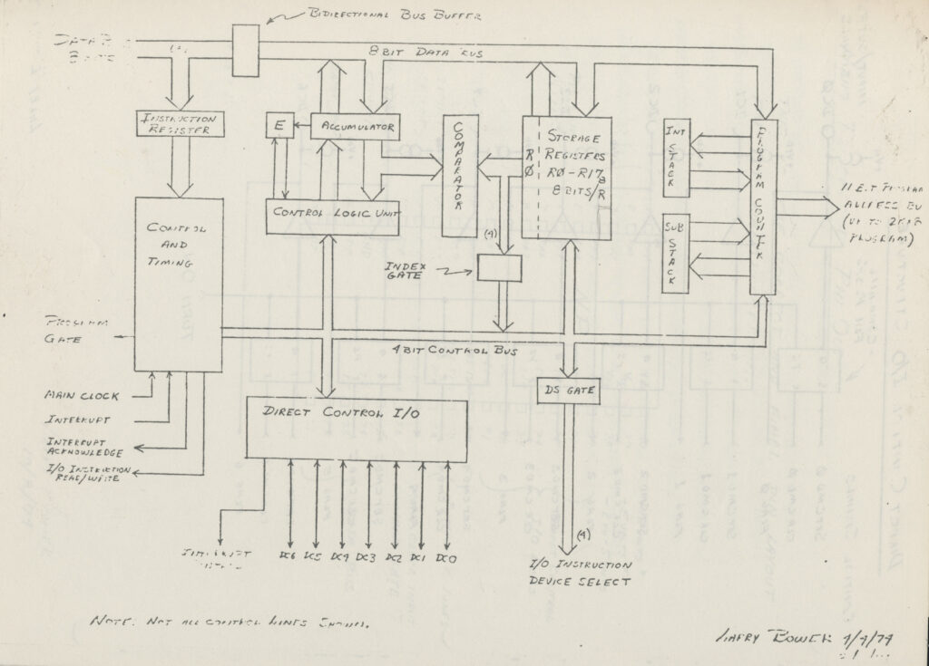
Handwritten Block diagram
The Nanoprocessor is interesting as it is specifically NOT an arithmetic oriented processor, in fact, it doesn’t even support arithmetic. It has 42 8-bit instructions, centered around control logic. These are supported by 16 8-bit registers, an 8-bit Accumulator and an 11-bit Program Counter. Interface to the external world is via an 11-bit address bus, 8-bit Data bus and a 7-bit ‘Direct Control’ bus which functions as an I/O bus. The nanoprocessor supports both external vectored interrupts and subroutines. The instructions support the ability to test, set and clear each bit in the accumulator, as well as comparisons, increments/decrements (both binary and BCD), and complements.
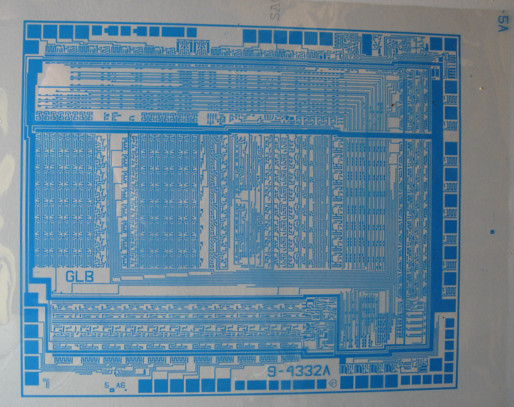
Here is one mask (Mask 5 of 6) for the prototype Nanoprocessor. You can see its simplicity. On the bottom of the mask you can see the 11-bit address buffers and Program Counter
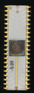
2.66MHz 1820-1691 – note the -5V Bias Voltage marked on it
The Nanoprocessor required a simple TTL clock, and 3 power supplies, a +12 and +5VDC for the logic and a -2VDC to -5VDC back gate bias voltage. This bias voltage was dependent on manufacturing variables so was not always the same chip to chip (the goal would be -5VDC). Each chip was tested the and voltage was hand written on the chip. The voltage was then set by a single resistor on the PCB. Swapping out a Nanoprocessor meant you needed to make sure this bias voltage was set correctly.
If you needed support for an ALU you could add one externally (likely with a pair of ‘181 series TTL). Even with an external ALU the Nanoprocessor was very fast. The projected cost of a Nanoprocessor in 1974 was $15 (or $22 with an ALU), In late 1975 this was $18 for the 4MHz version (1820-1692) and $13 for the slower 2.66MHz version (1820-1691).
At the time of its development in 1974-1975 the Motorola 6800 had just been announced. The 6800 was an 8-bit processor as well, made on a NMOS process, and had a maximum clock rate of 1MHz. The initial cost of the 6800 was $360, dropping to $175, then $69 with the release of the 6502 from MOS. By 1976 the 6800 was only $36, but this is still double what a Nanoprocessor cost
An early ‘slide deck’ (the paper version equivalent) from December 1974 sets out the What Why and How of the Nanoprocessor. The total cost of its development was projected to be only $250,000 (around $1 million in 2020 USD). The paper compares the performance of the Nanoprocessor to that of the 6800. The comparisons are pretty amazing.
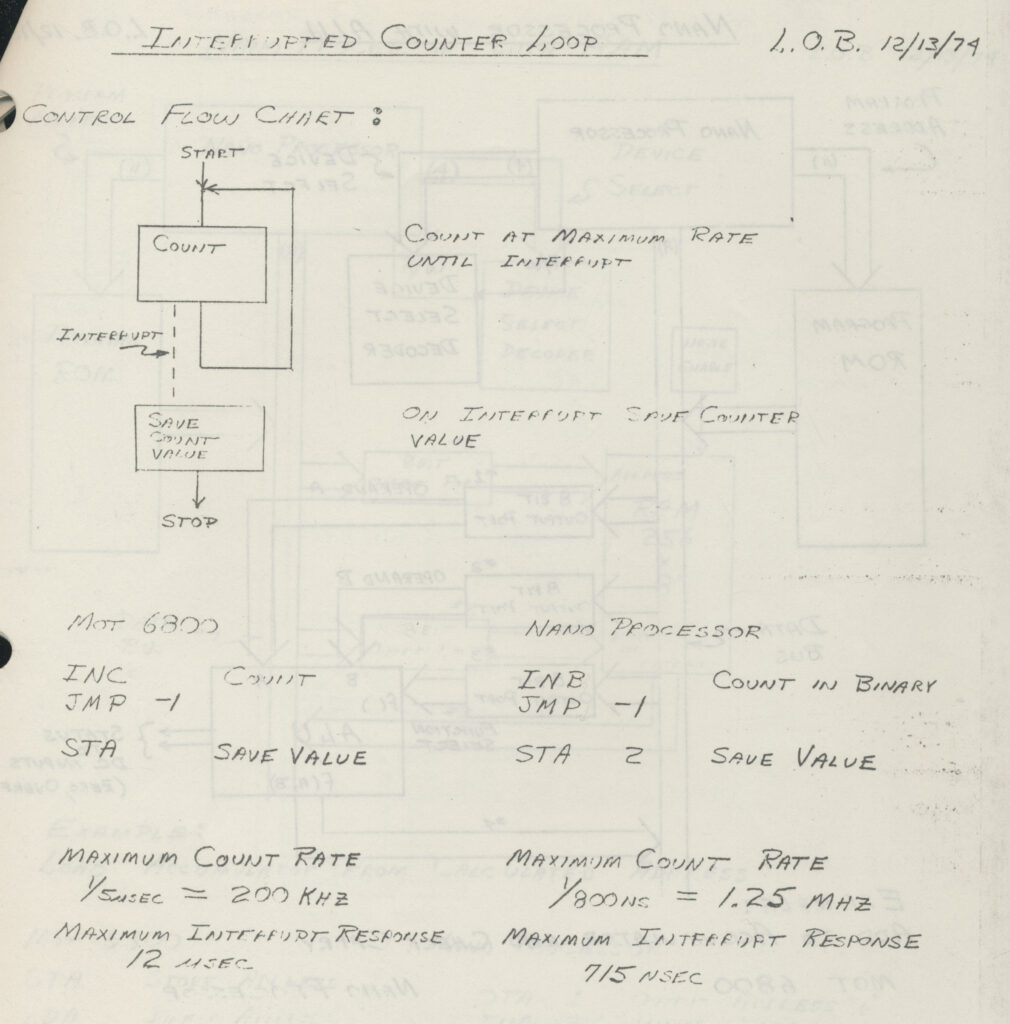
Interrupted Count Benchmark
For control processing interrupt response time is very important, the Nanoprocessor can handle interrupts in a max of 715ns, compare that to 12usec for the 6800. The clock rate of the Nanoprocessor is 4 times faster but the efficiency of its interrupts and instructions are what really provides the difference here.
The clock rate difference (1MHz vs 4) really shows here, but the Nanoprocessor is also executed 3 times the instructions to do the same task, and still is faster.
Even using an external ALU compared to the Motorola’s internal ALU, the nanoprocessor is better then twice as fast (thanks here to its much higher clock frequency)
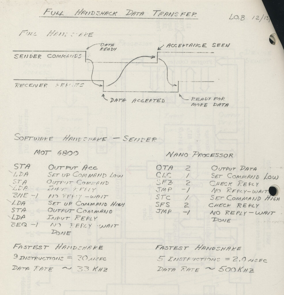
Full Handshake Data Transfer. Interfacing to the outside world was the main driver of the Nanoprocessor. Here we see that it can ‘talk’ to other devices much faster then the 6800
All instructions on the Nanoprocessor take 500ns to execute compared to the 1-10u for the 6800.
Today we do benchmarks based on framerates in games, or render times, but you can see that benchmarks were even important back then. How fast a processor could handle things determined how fast the printer could be, or how fast it could handle external data coming in. It’s no wonder that the Nanoprocessor continued to be made into the late 1980’s and many of them are still in use today running various HP equipment.
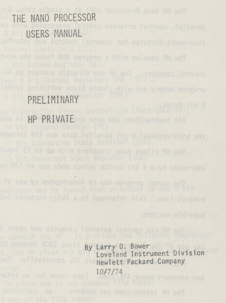
Nanoprocessor User Manual – October 1974
A big thank you to Larry Bower, the project lead and designer of the Nanoprocessor, who donated several prototypes, a complete mask set, and very early documentation on the Nanoprocessor (amongst some other goodies)
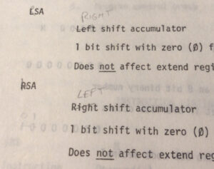
Documentation so ealy it has many hand written parts, and some corrections. This had to be a very annoying oops if it wasn’t caught early on. Even Engineers get their left and right mixed up on occasion