The Story of the Soviet 8080 Processor – The 580
Before beginning the history of the Soviet 580 series microprocessor, we need to say a little bit about the level of Soviet computing technology before the advent of integrated microprocessors. This is really a topic for a separate article, so just two facts.
This article is largely from guest author Vladimir Yakovlev, translated from Russian, and edited/expanded by me. It is part of a series on Soviet microprocessors that started with the Soviet T34 Z80 article.
In 1950 the “Small Electronic Computing Machine” (SECM) was made in the USSR. It should be noted that in the USSR this computer was launched at a time when there was only a few computers in Europe, the English EDSAK, launched just a year earlier and Zuse’s Z4 in Zurich in ~1947. But the processor of SECM was much more powerful by parallelizing the computational process.
In the creation of the SECM, all fundamental principles of computer creation were used, such as the presence of input and output devices, the encoding and storage of the program in memory, the automatic execution of the computation based on the stored program, etc. Most importantly, it was a computer based on binary logic used and currently used in computational engineering (the American ENIAC used a decimal system (!!!)).
In 1975, during the historic Soyuz-Apollo space mission, the control was carried out by the complex, which included the BECM-6 (Big Electronic Computing Machine), a direct descendant of SECM. This system allowed for one minute of flight computation time, while on the American side of the flight it took 30 minutes of computation.
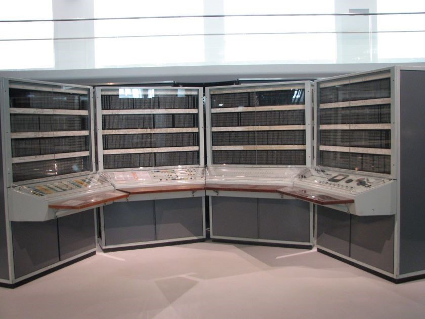
BECM-6 (Science Museum, London)
The real tragedy was the decision to produce IBM-360 clones in the USSR, that is, the transition to copying American architecture. I mean, obviously, whoever’s copying doesn’t have a chance to outrun (THe the USSR regularly added enhancements to Western designs). Copying has only one meaning – as a stage of learning. When you don’t have your own technology. Today, China is demonstrating the effectiveness of this approach. But the logical end of such an approach is still a shift to proprietary developments.
From that moment on, the Soviet Union was catching up.
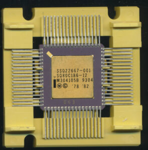
At the end of 1962, by the decision of the Government of the USSR, the Kiev Design Bureau was established in Kiev, later the Kiev Institute of Microdevices (KNIIMP), with an experienced plant. It was KNIIMP that was chosen to copy Intel’s products. The first task was to create a copy of the i8080 and was started in August 1976, just 2 years after Intel introduced the 8080 to the Western World.
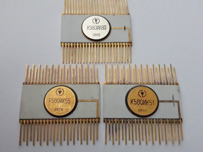
In 1977-1978, the first prototype chips were completed. The first basic set of the series contained three chips, K580IK80 (8080 CPU), K580IK51 (8251 USART) and K580IK55 (8255 PIO Controller).
They were produced in 48-lead metal-ceramic planar package. Contrary to popular belief, it is not a layer-by-layer copy of the Intel 8080 (some blocks are similar, but the layout and location of the bonding pads are significantly different). On November 6, 1980, the New York Times published an article “Soviet Gaining in Computers”. in which the author of article also reached this conclusion. These ran at 2MHz (500,000 ops/ec) and were made on a 6 micron NMOS process.
In 1981-1982 the package were replaced with the standard (Soviet pin spacing) DIP. Both versions for the domestic economy in plastic cases and for special applications in metal ceramics were released.
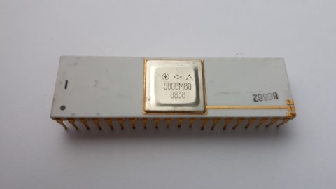
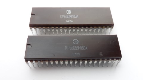
580VM80 – 1988 – Military spec
Around 1983, the names were changed from IK80 to VM80, IK55 and IK51 to VV55 and VV51 respectively. The additional letter “A” denotes an upgraded version of the processor from the extended base set of the series. In this variant, the speed was increased to 2.5MHz 625,000 op/s, the area of the die was reduced by 20%, (resulting from a process shrink to 5 microns) and the periphery of the crystal was redesigned.
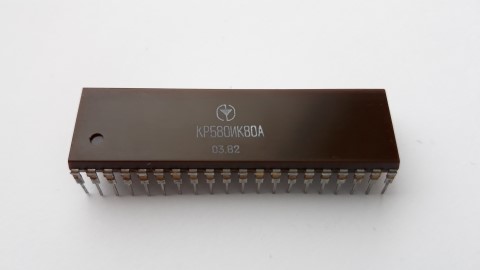
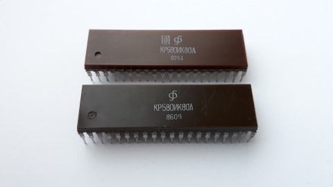
KR580IK80A – 2.5MHz – 1982 – “KWAZAR” (KIEV, UKRAINE)
The 580 series was produced by many of the Soviet IC design houses, for many years. Including, Kvazar, Electronpribor, Rodon, Kvator and Dnepr.
KR580IK80A “ELECTRONPRIBOR” (FRYAZINO, RUSSIA)
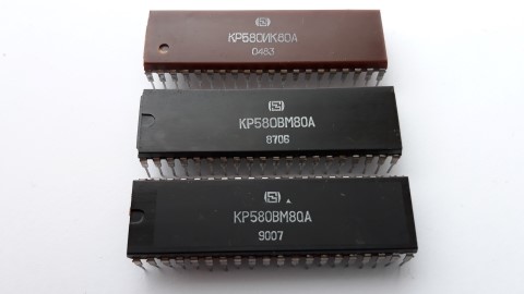
( “O” – pre-production sample)
“KVANTOR” (ZBARAGH, UKRAINE)
“RODON” (IVANO-FRANKIVSK, UKRAINE)
Top package is a early (1983) ‘Chocolate’ Brown PDIP
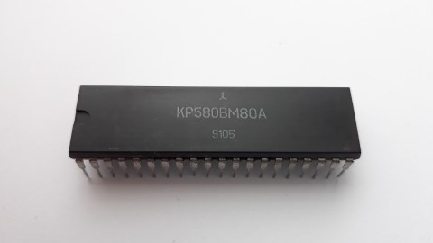
Late Production (1991) KR580VM80A – “DNEPR” (KHERSON, UKRAINE)
Chips manufactured for export were marked with the inscription Сделано в СССР and didn’t have the logo of the manufacturer. The ‘manufacturer’ was the USSR, as that was more important then which state enterprise it came from, as a matter of national pride.
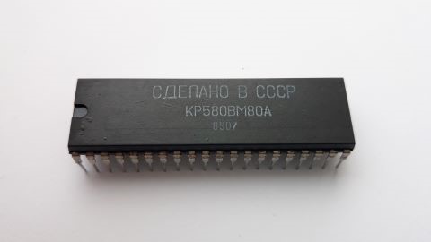
Export version (for Export to other Soviet Aligned countries)
In a sense, reproduction of microcircuit analogues is akin to a very high quality translation of foreign literature into native language. It is necessary not only to completely transfer the purpose of the product itself, but also to make it technologically compatible for the domestic producer. This is a very difficult task.
While the 8080 and 8086 microprocessors were at issue, the KNIIMP was successfully performing its task. But once Intel developed and started the 80286 and then the 80386, the Soviet Union was unable to produce similar microprocessors.
It can be argued that Intel Vice President Robert Noyce’s suggestion has been fully realized – the Soviet Union had fallen behind the United States in the development and production of modern microprocessor circuits forever. Even to this day Russia continues to make variants of Western processors, from the MCS-96 series, to Microchip PIC17’s. It should be noted that they did make a myriad of somewhat custom microcontrollers for specific tasks, that did not have direct Western Analogs (though sometimes they claimed these devices to be analogs of chips that they were not, in order to meet the direction of ‘copy the West’)