The Intel N60066: Unwrapping a Mystery
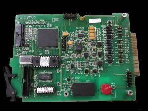
Fischer & Porter 53MC5 – The beginning of the Mystery
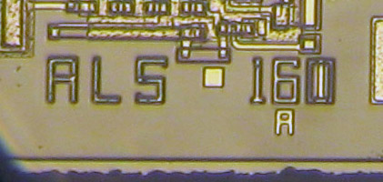
One day last summer, I was browsing the deep dark corners for processors, a fun, yet dangerous activity. I happened upon a lot of PCBs from some older industrial automation equipment. No real information was provided (those buying these boards clearly would already know what they needed). They did however have a RTC, an EPROM a 16MHz crystal, and a large 84-pin PLCC. That PLCC was marked as an Intel N60066. Seeing such a large chip, surrounded by such components almost always means its some sort of processor or microcontroller. The problem is, there is no known Intel 60066 part. The chips were all made in the late 80’s and early 90’s and had 1980 and 1985 copyrights. A 1980 copyright typically screams MCS-51, as that was when it was introduced and nearly all such chips bear an Intel 1980 mark.
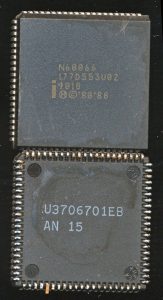
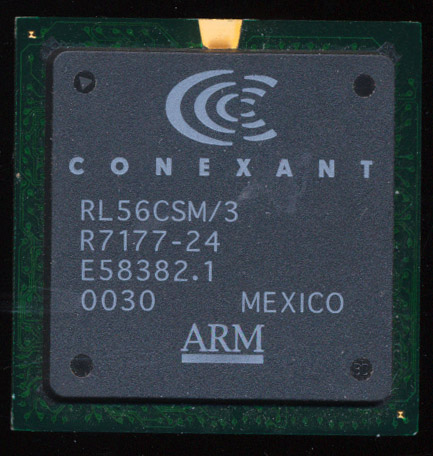
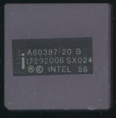
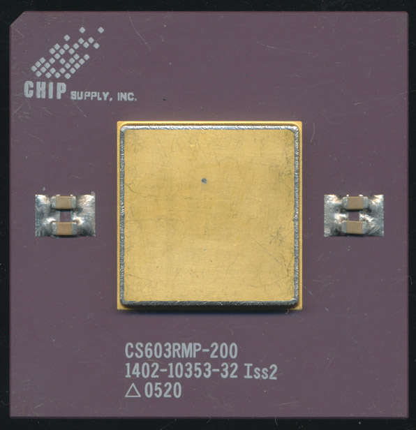
Intel N60066
The boards themselves were dated from 1990 all the way to the early 2000’s (I bought a lot of them, another problem I have). Some had the part number 53MC5 and the logo of Fischer & Porter. Fischer & Porter has existed since the 1930’s and was a leader in instrumentation. They were bought by Elsag Bailey Process Automation (EBPA) in 1994 which itself was swallowed up by ABB in 1999. The boards design was largely unchanged through all of these transitions. Searching for documentation on the 53MC5 part number (its a Loop Controller) didn’t yield details on what the N60066 was unfortunately. The only thing left to do was to set it on fire…
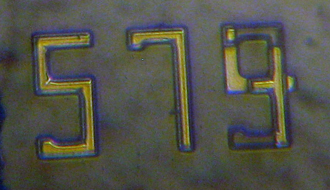
Unfortunately this is the only way I currently have for opening plastic IC’s (I need to get some DMSO to try apparently). After some careful work with the torch and some rough cleaning of the resulting die it was readily apparent that this was an MCU of some sort. The die itself was marked… 1989 60066. This wasn’t a custom marked standard product, this was a custom product by Intel for this application, a very surprising thing indeed. Unlike other companies such as Motorola, Intel was not well known for custom designs/ASICs. This wasn’t their market or business plan. Intel made products to suit the needs they saw, if 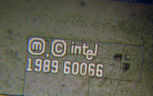 that worked for the end user, great, if not, perhaps you could look elsewhere. They would gladly modify specs/testing of EXISTING parts, such as wider voltage ranges, or different timings, but a complete custom product? Nope, go talk to an ASIC design house. Its likely Fischer & Porter ordered enough of these to make it worth Intel’s effort.
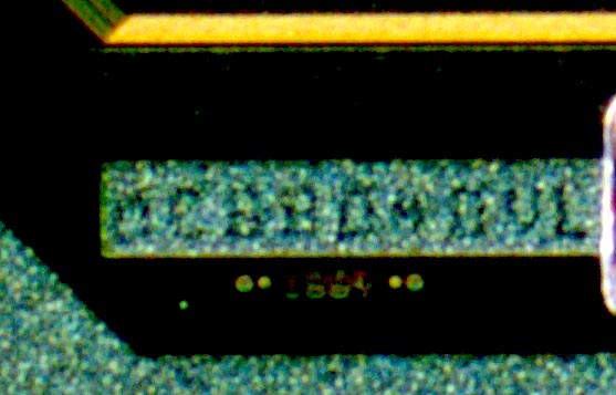
Knowing this was an MCU and suspecting a MCS-51 further searching revealed the answer, and it came from the most unusual of places. In 2009 the US NRC (Nuclear Regulatory Commission) determined there was no adequate Probabilistic Risk Assessment (PRA) for Digital systems in their agency, so set about determining how best to calculate risk of digitally controlled systems. They analyzed a system used to control feedwater in nuclear reactors. These are critical systems responsible for making sure the reactor is kept with the right amount of cooling water at the right time, failure of course is not an option. The 53MC5 is what is used for controlling the valves. In this document we find this nugget:
The controller is an 8051 processor on board an application-specific integrated circuit (ASIC) chip that performs a variety of functions.
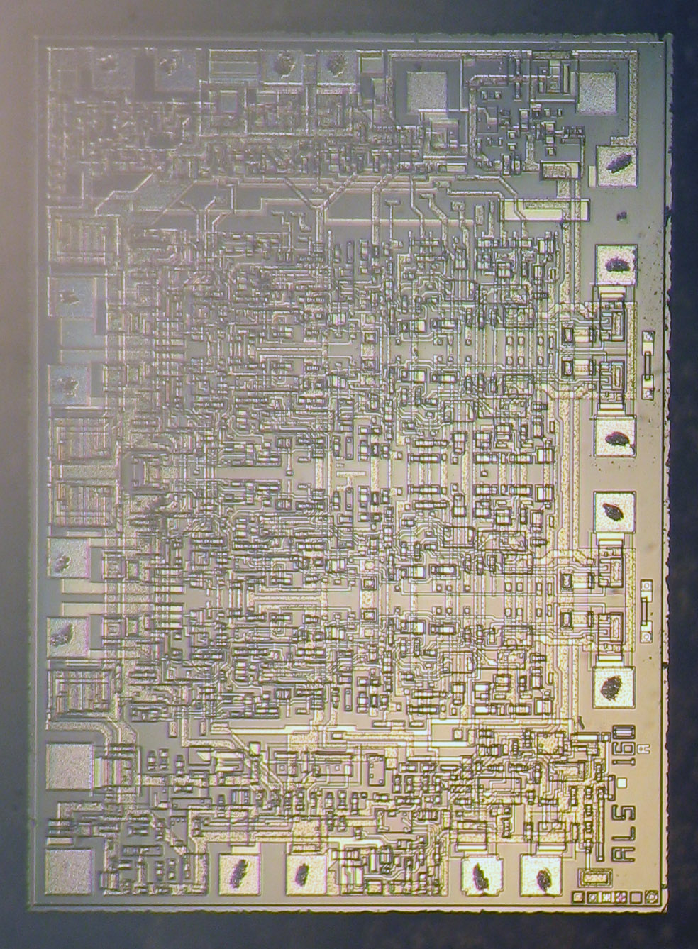
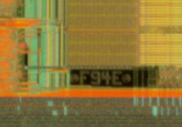
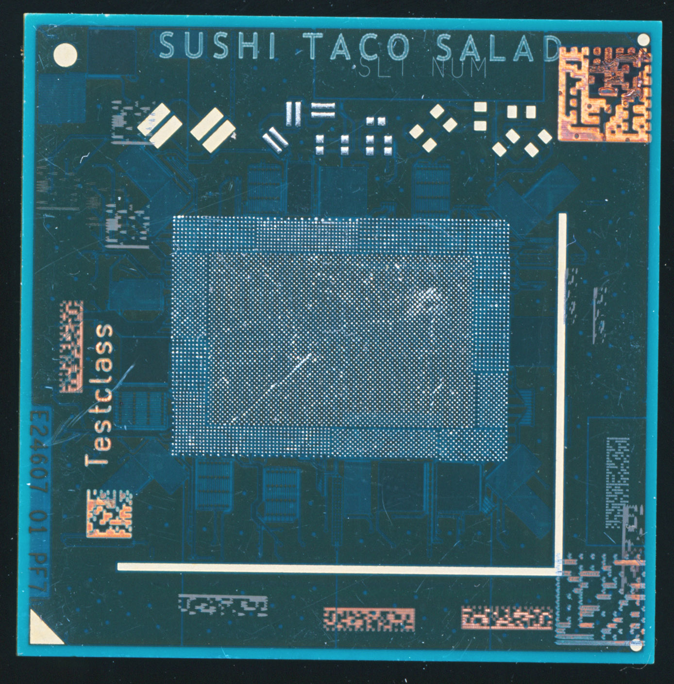
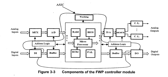
Well that certainly helps, it is indeed a custom ASIC based on an 8051. The report also provided a diagram showing the ASIC system. This is an 8051 core with RAM/ROM (normal) as well as a Watchdog timer, a PAL, I/O Buffers, and Address Logic.
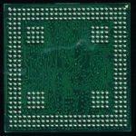
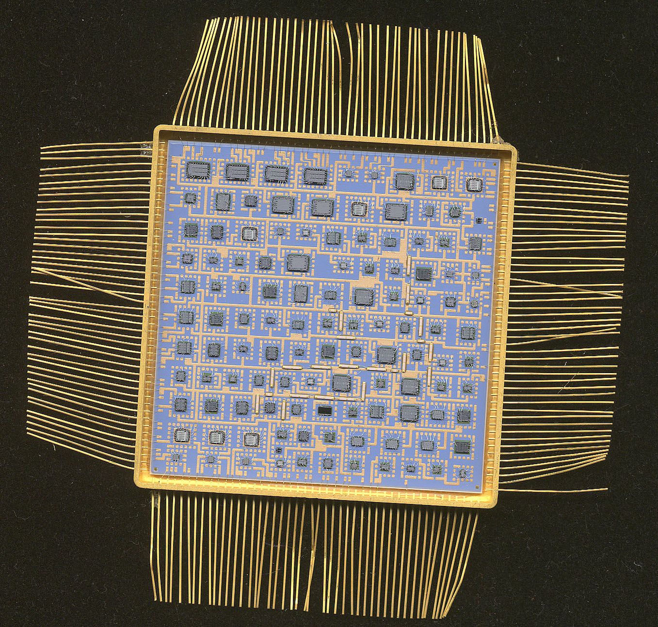
I sent a couple of these chips to my friend Antoine in France for a proper die shot, which he is quite amazing at.
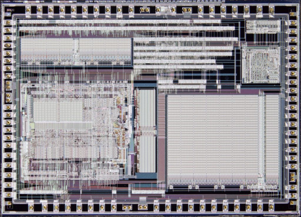
Intel N60066 die – 8051 core on the left. Die shot by Antoine Bercovici
The 8051 core is on the left of the die, with its RAM/ROM. A very large PLA occupies the bottom right side of the day. In the upper right is presumably the external watchdog timer for the ASIC. The lines crossing the die mostly vertically are a top metal layer used for connecting all the various sections.
The hunt for a new CPU/MCU is part of the thrill of collecting. The satisfaction of finding out what a mystery chip is can be worth many hours of dead ends in researching it. Its not common to have to go to the NRC to find the answer though.
Posted in:
CPU of the Day