
Tiered up for 3D-FPGAs: The Story of the Tier Logic FPGA-ASIC
100K LUT Tier Logic FPGA TL1F100 on the left and TL1A100 ASIC on the right
This is the CPU Shack Museum, but occasionally I find a chip thats not really a CPU but is of such interest that I keep it, especially if its novel and relatively unknown. So today we have a bit of the story of Tier Logic. Tier Logic set out to make FPGA (Field Programmable Gate Arrays) better, and to make the transition (or choice) between them and ASICs (Application Specific Integrated Circuit) easier.
FPGA’s are great for smaller product runs, they are configurable, and relatively easy to reprogram, designs can easily be updated/tested with no additional cost. FPGA’s however are large in terms of die area, power budgets, and cost per chip. ASIC’s on the other hand, take longer to develop (re-spinning silicon every time an error is found) and have a much larger upfront cost, as well as an entirely different tool chain to design with. They are however smaller, use less power, and once the design is finalized, the per unit cost is very low. This presents a dilemma in design, which should one choose for a project? What if you didn’t have to choose? What if you could have the flexibility of an FPGA, and the benefits of an ASIC all at once?
It is exactly this that Tier Logic set out to do. Tier Logic was founded by FPGA process-technology pioneer Raminda Madurawe (from Altera) in 2003 and was led by Doug Laird, a founder of Transmeta (famous for the Crusoe VLIW processors). For 7 years they worked to design a solution, working in what is known as ‘stealth mode.’ Stealth mode is a way for companies to work quietly, with little to know PR, until they have a product ready to release. Often the company exists but is completely unknown to outsiders. This has some definite benefits, there is no constant barrage of having to answer/report to the media and others, and their is less risk of someone seeing what you are doing and trying to beat you to market to it. Seven years, however, is a very long time to be in stealth mode, and the reason for this is Tier Logic not only was inventing a new style of FPGA/ASIC, they had to develop a new silicon process to make it work.
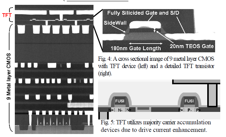
Cross section showing TFT layer (180nm) on top of 9 90nm CMOS layers with Cu-interconnects)
In most traditional FPGAs SRAM is used to store configuration information (essentially Look up Tables that determine where all the gates are connected/routed). These SRAM cells are rather large on a standard CMOS process, and are integrated amongst all the logic on the die. This results in larger dies, larger power consumption, and more expense. Tier Logic wanted to seperate the SRAM from the rest of the design, allowing all the logic to be much more compact. The process they developed (with Toshiba, their fab partner) was to use a standard 90nm CMOS 9 Metal layer process, and use 8 of those layers for the FPGAs logic, on top of this they added a layer of TFT (thin Film Transistors) based SRAM cells (the 9th layer as then used to connect these to the logic below). Each TFT SRAM bit uses 9 transistors, and the Tier Logic design used 230 million of them (to give around 26Mb of SRAM) to support is 100k LUT design. TFT SRAM isn’t anything new, but integrating it onto a CMOS process was. TFT SRAM is usually made at over 400C in manufacturing, which is more than standard CMOS with Cu interconnected can handle without degradation, so Toshiba found a way around this, allowing the TFT transistors to be built on the same die with no ill-effects. The TFT layer was done on a 180nm size (twice as large as the underlying metal layers) using technology from Toshiba’s 65nm node. This made for a FPGA that was much smaller, and had much smaller power budgets then a traditional FPGA as well as being much faster, 1.8-3.5 times faster than a traditional FPGA on the same process. That’s 1-2 process nodes of improvement for free. Tier Logic wasn’t done however, having the SRAM completely separate (top layer, thus being a 3-D part) allowed them to do something quite remarkable.
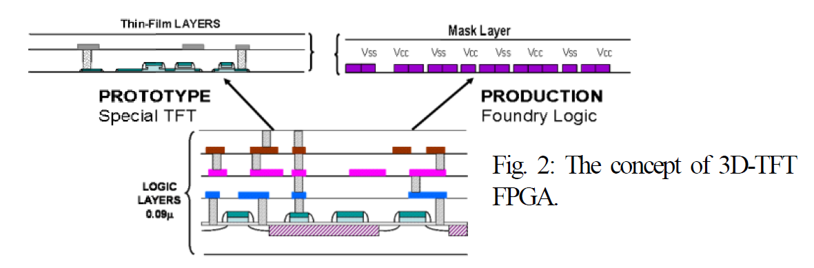
Only one layer has to change to switch from FPGA to ASIC
If a customer wanted to convert their FPGA design to an ASIC, the TFT SRAM layer is omitted and the 9th layer becomes a MaskROM layer, essentially hard coding what would have been stored in the SRAM cells. Timing and logic remains identical, and it could be done for less then $50,000 and 4 weeks time. Customers could also develop an ASIC using the FPGA version, and FPGA tool chains (specifically Mentor tools) which are industry standard, and then when they are ready for the final version, have the ASIC created. Tier Logic held wafers at Metal Layer 8, so that they could be finished as an FPGA or ASIC without having to fab/test all the logic for every device. For large orders (over $100,000) Tier Logic even offers to custom package the parts to match the pin-out of your existing FPGA design (whether it was a Xilinx, Altera, or other FPGA part).
Tier Logic had plans for larger and faster designs as well, including integrating switch fabric into the 3-D mix.
In March of 2010 Tier Logic exited stealth mode, and with early orders in hand, went public with their technology and products. They needed funding of $20 million to ramp up the business and begin the 3D-FPGA revolution, but for reasons that are still unclear, that funding never came, and on July 16th of that year, only 5 months after exiting stealth mode, Tier Logic was closed. Its possible this was a result of having been unknown for so long, one wonders if they would have been more successful if they had been public earlier. Its also possible that the existing FPGA companies were not a fan of what Tier Logics technology could have caused in the market and pressured customers/investors away form them, but we likely will never know. Perhaps most tragically is the technology was never marketed. The relevant patents ended up in the hands of Callahan Cellular LLC, a shell company of Intellectual Ventures, which makes the majority of its money not from making actual products, but by licensing and litigation the vast portfolio of patents they have acquired. They are the 5th largest patent holder in the US and often referred to as a ‘Patent Troll’ due to their techniques for extracting revenue by litigation.
FOr a company that exited in the public eye for but a fleeting moment, it is nice that the memory and history can be preserved in having a few of the only samples made of their technology. Truly it was top tier engineering.
June 18th, 2019 at 8:14 am
Hello,
Very interesting read, thanks for the article 🙂
Rik
July 4th, 2019 at 1:36 pm
Wow, that’s really sad. One of the many inefficiencies of capitalism, despite there not supposed to be any. Aren’t there cost disadvantages though, to replacing a real ASIC with basically-an-FPGA-but-with-ROM? On smaller runs I suppose it’s OK, and I suppose it reduces testing cost. But am I right in thinking it’s not cut out for really big products?
July 4th, 2019 at 1:41 pm
It makes the development of the ASIC much cheaper, as you can start with a FPGA based design, do all your testing their, and THEN put it to silicon. Its a bit more cost then a pure ASIC, but there is a lot of savings on the front end, so time to market and initial cost go way down.