CPU of the Day: National Elentari x86 and What Lies Beyond – Part 1
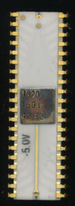
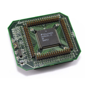
National Semi NS486SXF-25 Rev C0 -1999
While I was casually reading an issue of ‘Boot’ Magazine from 1997 I was sent down the rabbit hole by a mention of a processor in a small blurb in a footnote of an article. Just a few lines really is all, but about a processor I was not familiar with, an x86 one at that! So nearly a month later, I have emerged from the rabbit hole. We will begin not with what sent me to the hole in the first place, but when and where the hole itself came from, and that is the year 1995, the place? National Semiconductor.
As mentioned in the 486 Overclocking article, the 1990’s were a boon for up and coming x86 processors. In some ways it was similar to the processor bonanza of the 1970’s but centered on x86. Many companies wanted to have a go at the x86 architecture market. National Semiconductor was of course interested in making something with x86 as well. They rightly decided that a head to head competition with Intel for mainstream PC processors wasn’t the best idea, but that embedded computing, low cost set top box (as they later would become) and ‘Network PC’s’ would be a good market. The goal was to design a simple efficient x86 processor and integrate it with many peripherals, and sell it for $20-30 each.
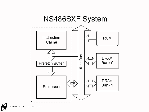
Elentari Core. 16-byte Prefetch Buffer, 1K Cache ,16-bit Data Bus and support for 2 8M DRAM Pages
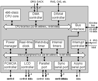
NS486SXF/L Block Diagram (SXL omits blocks in dashed lines)
The core project began in very early 1995 (or late 1994) and was known as the Elantari, Queen of the Stars in Lord of the Rings Mythology. The Elantari (aka the ESF94001) had three priorities in its development (in order): 1) Schedule, 2) Low Cost, 3) Performance. Time to market was essential, even at the expense of performance optimization. The core (which the Marketing dept quickly renamed to the NS486) was to be a 486 compatible core (using protected mode only) with some optimizations and was organized officially under a new unit at National Semiconductor called the Arador Unit (someone really liked LotR). Target speed was 25MHz at 5V on Nationals 0.65u process using a very simple 3-stage pipeline (Fetch/Decode, Execute, Write Back).
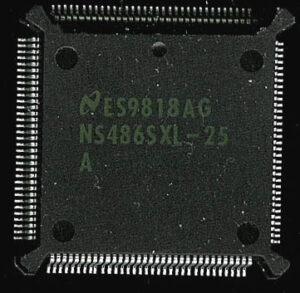
NS486SXL-25 No Rev Marked 1996 (courtesy xSecret)
Balancing cost and performance meant that die area should be minimized, as this effects yields and parts per wafer. This, on a 0.65u process, allowed for a small area of cache. National ended up, after a fair amount of analysis, going with a 1K direct mapped instruction cache (that can bus snoop) and a 16 byte prefetch buffer. This is in great contrast to the Intel 486 which had a 8KB unified cache (and 16K on later 486s). But for embedded use instructions have a better performance increase when cached then data. Cache also presents some difficulties with real time computing, as its difficult to know how long an operation will take if you don’t also know whether it s from cache or the main memory. National provided a method on the NS486 to load and lock the cache with a set of instructions that would ALWAYS operate out of cache. This combined with assigning one DRAM page to Data, and another for stack use, made timing more predictable and consistent when needed. As part of the development process National used IP they had licensed from another IIT, whom had earlier designed a 486 class processor. IITs IP was not used in the NS486 itself, but was used in helping debug, design and develop it and its testing environment.
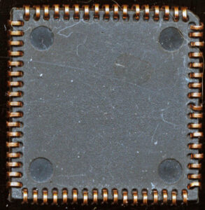
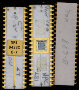
NS486SXL-25 Rev A – SXL unique die – 1998
The NS486 core lacked both a FPU and MMU, and had a 16-bit data bus. This allowed for a fairly small core size. The core alone took up about 256,000 transistors (roughly half of what the Intel 486 integer core used) and on the initial 0.65u 3-layer process results in a core die size of 29.6mm2 including the cache. (the SXL die with limited peripherals pushed that to around 64mm2) The short pipeline greatly restricts the speed, it never made it above 25MHz (though 33MHz was apparently achievable.
National Semiconductor by this time had become dominate in integrated peripheral chips, led by its ‘SuperIO’ chip line, and it was this integration that made the NS486 unique. National designed two versions of the NS486, the NS486SXF with a full set of peripherals, and the smaller NS486SXL with a few less. The integration of peripherals was one of the most challenging aspects, the core itself is relatively simple, but adding other features, often with different clock and signal domains is much harder to design and test. This is where National’s expertise on SuperIO chips came in handy.
The other challenging aspect of a x86 design in the 1990’s was from the legal department. Intel claimed that even a clean design of anything x86 ‘MUST’ violate at least one Intel patent. National however had designed the NS486 from the ground up, including the microcode, AND as a backup, also possessed a license from Intel dating back to the 1970’s (it was that license that helped lead to the National/Cyrix merger).
| NS486SXF | NS486SXL | |
| Package | 160PQFP | 132PQFP |
| Cost | $25 | $15 |
| 486 Core |
X |
X |
| DRAM Controller |
X |
X |
| DMA Controller |
X |
|
| LCD Controller |
X |
|
| ISA Bus Interface |
X |
X |
| External Bus Master Controller |
X |
|
| UART/IrDA |
X |
X |
| ECP Parallel Port |
X |
|
| PCMCIA Controller |
X |
|
| Real-Time Clock, Timers |
X |
X |
| Programmable Interrupt |
X |
X |
| Reconfigurable I/O |
X |
X |
| Programmable Chip Select |
X |
X |
| 3-Wire Serial Peripheral |
X |
X |
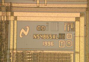
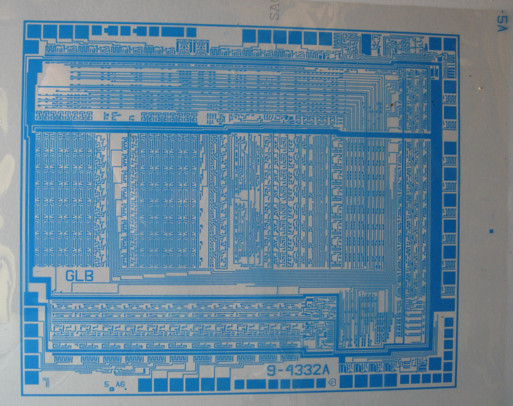
NS486SXL Rev A0 die – matches package markings – Still 0.65u (courtesy aberco)
Initially both the NS486SXL and SXF used the same die, with the SXL having some of the onchip features disabled. National planned on making a seperate die later for the SXL to further reduce costs. They did this in around 1998. Their goal was also to shrink the design to their upcoming 0.35u process but it is unknown if they successfully did this (dies from 1998 continue to be of the 0.65u variety).
Initial samples were available by early 1996, a rather quick development. The NS486 was well supported in both hardware and software. It supported a number of common real-time operating systems of the time, including pSOS+, QNX, VxWorks, and VRTX. It did not however support DOS, having no real mode support. In 1997 the NS486SXF was used to implement Jav Nanokernel, a Java based OS running the Java VM directly on hardware. Hardware vendors included PARVUS (NS486 based PC104 board), BCT (Dev Boards) and several others making ready made NS486 based SBCs. In November of 1996 National released a full Web Browser based Network computer Reference design using the NS486 called the ‘Odin’ This was the first sub-$200 web browser capable computer of the time.
NS486SXL die – Peripherals take up about a third of the die (die photo from aberco)
In 1997 things got a bit more interesting. National Semiconductor decided to merge (in all reality it was an acquisition) with Cyrix. The NS486 continued to be made, but by 1999 National listed it as ‘not recommended for new designs’ It would also appear that some things never really got finished. Datasheets up through at least Dec of 1997 were still ‘Preliminary’ though the silicon had been produced for sometime. Production of the NS486 continued well into the 2000s, with chips being made at least into 2003 and probably later.
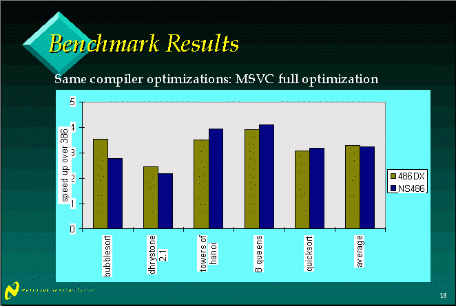
The NS486 Performance in integer tasks was pretty good. In some cases beating the Intel 486DX. THis is largely because of its optimized instruction timing, many are single cycle, much faster then other cores.
 At the time of its introduction it had little competition (in the x86 realm). Intel had the 386EX and AMD had an the 386SC (what later became the ElanSC300 line). Both of these were 386 class parts that were slower (and in the case of the 386EX) more expensive. Intel themselves did not have a good embedded 486 option largely due to lack of trailing edge fab capacity. Most of their fabs had been (or were being) converted to higher end processes to make new Pentiums and P6 chips, while their older fabs were filled to the brim with Intel’s then booming chipset business.
| ARM 610 | Motorola 68349 | Hitachi SH7032 | NEC V820 | MIPS LR33020 | Intel i960CA | AMD 386SC | Intel 386EX | NS486SXF | |
| Frequency | 20 MHz | 25 MHz | 20 MHz | 25 MHz | 25 MHz | 25 MHz | 25 MHz | 25 MHz | 25MHz |
| Dhrystone MIPS | 18 | 9 | 16 | 18 | 14 | 30 | 5.4 | 7.1 | 12 |
| FPU | No | No | No | Yes | No | No | No | No | No |
| MMU | No | No | No | No | No | No | Yes | No | No |
| Cache | None | 1K Inst | None | 1K Inst | 4K/4K | 1K Inst | None | None | 1K Inst |
| Periphs. | Some | Some | Some | Some | Some | Some | Full Set | Some | Full Set |
| Transistors | 359k | 550k | 593k | 380k | 700k | 600k | 335k | ?? | 500k* |
| Process | 1.0u | 0.8u | 0.8u | 0.8u | 0.7u | 1.0u | 0.7u | 0.8u | 0.65u |
| Price | $20 | $33 | $30 | $80 | $67 | $90 | $49 | $33 | $25 |
*Estimated Core = 256k Cache = ~50k
It was suggested that if National lengthened the pipeline of the NS486 to the then standard 5-stages, and moved it to their new 0.35u process that it could ‘easily’ hit 133MHz at 3.3V. But what embedded designer would want to have to deal with that fast of a processor? It would seem that the NS486 team had ideas beyond just the purely embedded market, as something more then the NS486 was their ultimate goal, and exactly what led me down this Rabbit hole……
In Part 2 we’ll look at what National developed from the NS486, and if it wasn’t for the MediaGX they acquired, very likely would have made it to market.
Posted in:
CPU of the Day