
IBM Blue Gene/Q: The Heart of a Supercomputer
Usually we find vintage processors here at the CPU Shack Museum, however, from time to time, we get our hands on something very new, and usually significant. If by significant one means the processor from a Top500 supercomputer then yes, it is significant.
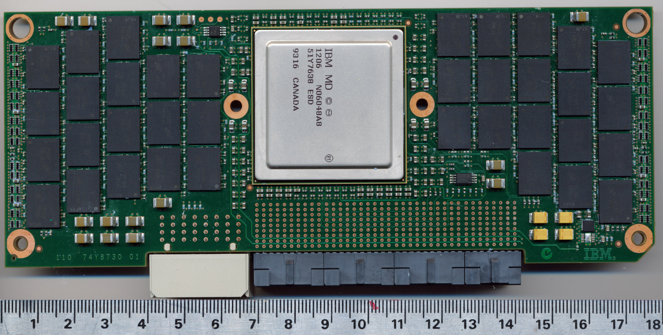
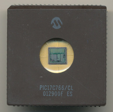
IBM 51Y7638 – Produced Early 2012 – Blue Gene/Q 1.6GHz 18 Core PowerPC-A2
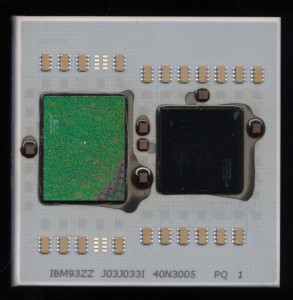
This is a Compute card from an IBM Blue Gene/Q (specifically the 6 rack BG/Q running at England’s Science & Technology Facilities Council Daresbury Lab in Cheshire). A Blue Gene/Q system is made up of these cards, 32 per ‘Node Card’, and 1024 per rack. This doesn’t count the I/O board which use a similar design and contains 8 Compute cards per rack.
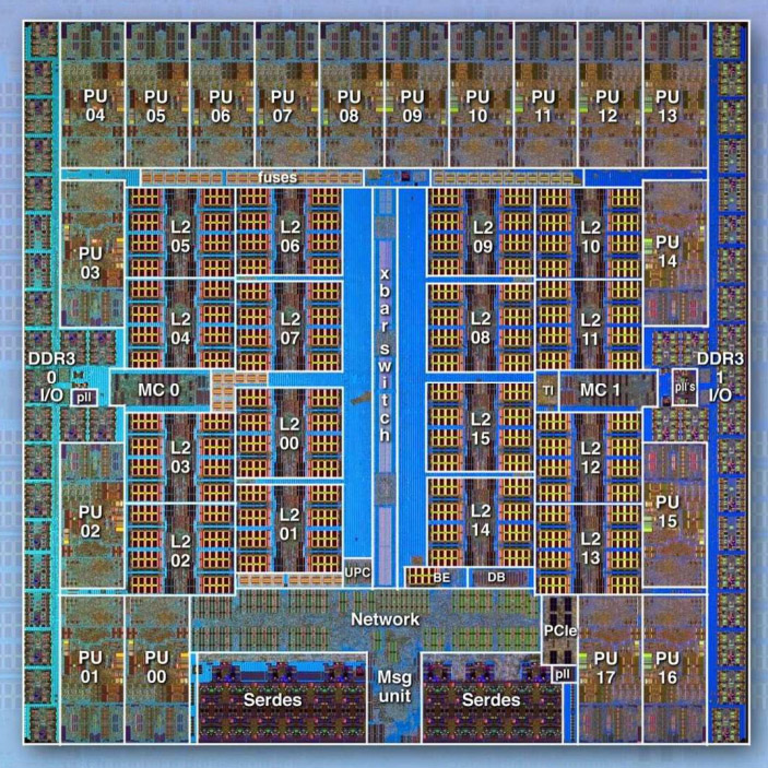
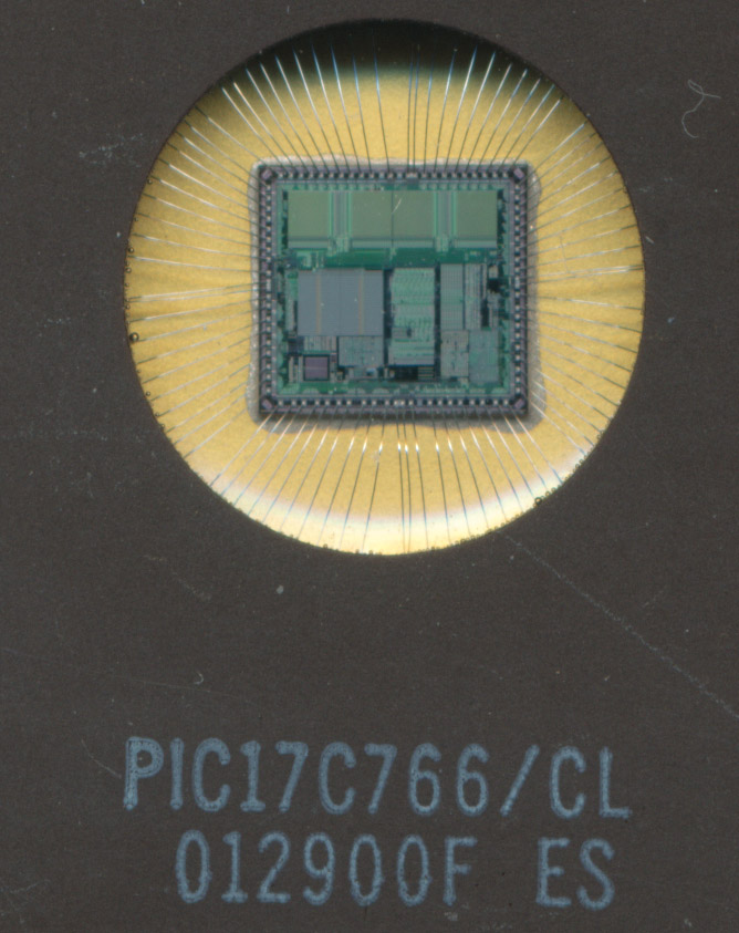
BlueGeneQ ASIC die shot
Each of the Compute cards contains a large ASIC (the large chip in the middle). This ASIC contains 18 PowerPC-A2 processor cores running at 1.6GHz. 16 of them are ‘User’ cores, 1 is for system management (handles interrupts message passing, etc) and the 18th is a spare, for increased fault tolerance. The ASIC also contains 32MB of shared L2 cache and a dual 1.3GHz memory controller for the 16GB of DDR3 memory on the card. All said this 45nm chip contains 1.47 Billion transistors, but only dissipates 55Watts, granted, that adds up when you have thousands of them.
A ‘basic’ system contains 4 racks, so 4096 compute cards (4128 if you count the the I/O boards). Together this is 65,536 user cores and consumes upwards of 85kW of power (this actually makes it one of the most efficient super computers available).
So how do these cards become available? Simply put when you have so many in a system, statistically you are going to have failures, and somewhat frequently. IBMs target failure rate, based on a 96 rack system (which is massive) is 70 hours. That’s one failure every 3 days. At this point the common reaction is to express shock at the dismal reliability of such a system, however, lets put it another way, that’s one failure out of 98,000+ Compute cards (yes there are other failure points but for the sake of argument we’re using just the compute cards). If you run an IT department that services nearly 100,000 computers and you only have to fix something twice a week, there is a good chance you should get a raise.
Posted in:
CPU of the Day


