
A history of the EPROM in the Soviet Union
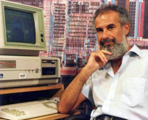
Dov Frohman
In 1971 Intel came out with the first memory that could be not only programmed by the user, but could be erased with UV light and programmed again. This was the 1701 EPROM (quickly revised into the 1702 EPROM and 1702A). It was 2048 bits (256×8), used PMOS, and required three voltage (+5V, +12V and -12V) to operate, and each data line required a strobed -48V pulse for programming.
The 1701 was introduced to the world in the May 10, 1971 issue of Electronics Magazine in an article written by Dov Frohman, the inventor of the EPROM. Today Intel is more known for, and remembered by their microprocessors, but until the early 1980’s it was EPROM’s that carried the company. They accounted for the largest share of profits at Intel for over a decade.
K505RR1
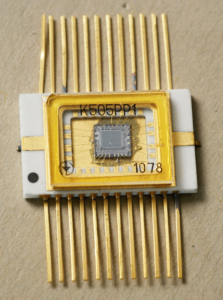 Soviet K505RR1 – 1978 |
 Intel 1701 – Unmarked |
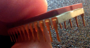
The first EPROM chip produced in the Soviet Union was the K505RR1, developed by the Kyiv Research Institute of Microdevices and manufactured by the Kvazar factory in Kyiv, Ukraine. The chip is a 2048-bit (256×8) electrically programmable read-only memory with ultraviolet erasure. It is an analogue of the 1702А.
They supported up to 20 (they wore out quite quickly) overwrite cycles and had a data retention period in on state of not less 5000 hours. This is one of the only EPROM chips manufactured in the flat pack package. NEC made a 2Mbit flat pack EPROM in the 1990s, quite a strange beast.
 |
 |
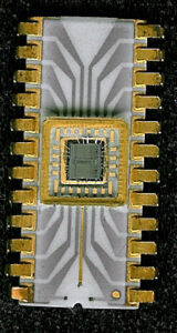
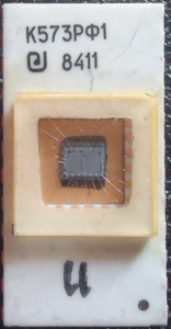
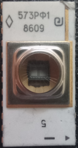
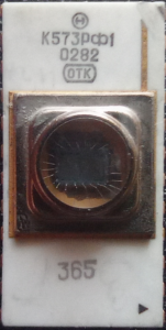
K573RF1
Analogue of the i2708. The microcircuit is a read-only memory device with a capacity of 8 Kbit (1024х8). Supply voltages of 12v, 5v, -5v. Data Retention period in on state is not less 15000 hours. Number of write cycles at least 100. (a nice improvement over the previous generation)
Microcircuits were manufactured at two factories: Novosibirsk Factory Vostok and Novosibirsk Electrovakuum Factory (NEVZ). The ‘3’ logo is an export version.
 NEVZ – 1984
|
 NEVZ military grade version(without letter K + rhombus) -1986 |
 Vostok – 1982
|
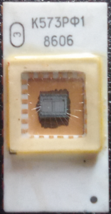 Export – 1986
|
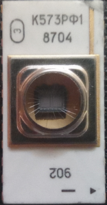 Export – 1987
|
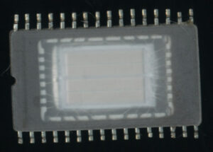
On microcircuits with a metal cover, you can see that a part of the conductor connecting this cover and GND pin has been mechanically removed. In electrochemical coating, it’s necessary that all surfaces on which gold is deposited in this case be connected to each other. But the K573RF1 chip has three power supplies. And minus 5 volts is applied to the die substrate. Part of the conductor has been removed to avoid a possible short circuit.
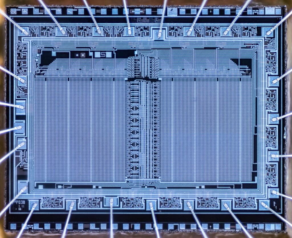
It’s clearly seen that the die of K573RF1 is divided into two memory blocks.
In the manufacture of dies, it happens that several memory cells turn out to be damaged. The manufacturer blocks access to damaged part of the die by connecting one or two input addresses to ground or a power supply. Either guarantees the operation of only half of the data bus of the microcircuit. K573RF11, K573RF12 have an information capacity of 4 Kbit (512×8) , K573RF13, K573RF14- 4 Kbit (1024×4).
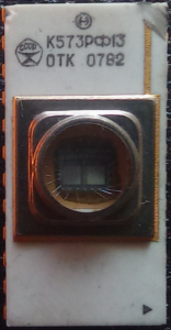 K573RF13 |
 K573RF14 |
 K573RF14 |
(I do not have any example of the 573RF11 or 573RF12 but would love to add some)
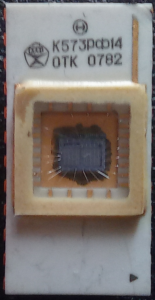
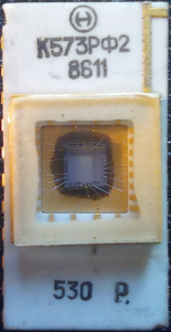
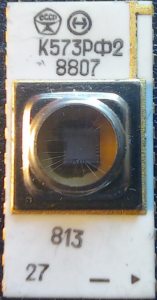
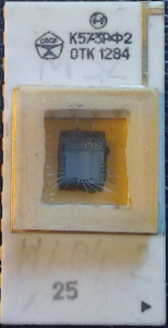
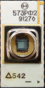
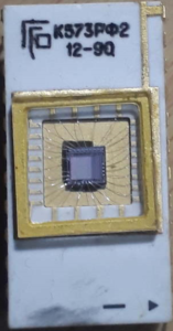
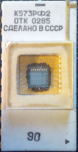
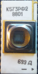
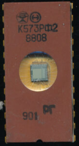
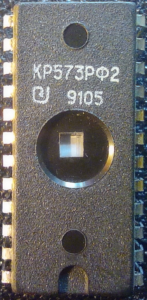
K573RF2
Analog of the i2716 with capacity of 16 Kbit (2048х8). Supply voltage +5v. Data retention period in on state is not less 25000 hours. Number of write cycles at least 100.
Initially, microcircuits were produced in white ceramic packages, the same as those of the K573RF1. Only the need to remove part of the conductor on top was no longer there. The die’s substrate was now connected to ground.
 |
 |
 |
 |
 |
 |
Many microcircuits were produced with the State Quality Mark of the USSR.
You can read more about this here:
https://www.cpushack.com/2014/04/22/soviet-k573rf23-quality-mark-cccp/
On some microcircuits, you can see the abbreviation OTK. This is the mark of the Technical Control Department. In economy of the Soviet Union, Technical Control Departments (Russian: OTK) were and are in charge of quality assurance of production. In the late Soviet Union the OTK existed in all socialist enterprises.
Manufacturing factories are the same that produced K573RF1. Only in the early 90s did a new manufacturer appear. Research and Production Cooperative «KVANT» (Latvia).
 |
 |
With and without production date
 |
 |
Part of the K573RF2 was produced without the manufacturer’s logo
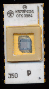
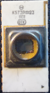 573RF23 |
 573RF24 |
Also, as in the case of K573RF1, there were half-capacity K573RF2 chips. K573RF21, K573RF22 have an information capacity of 8 Kbit (1024×8) , K573RF23, K573RF24- 8 Kbit (2048×4).
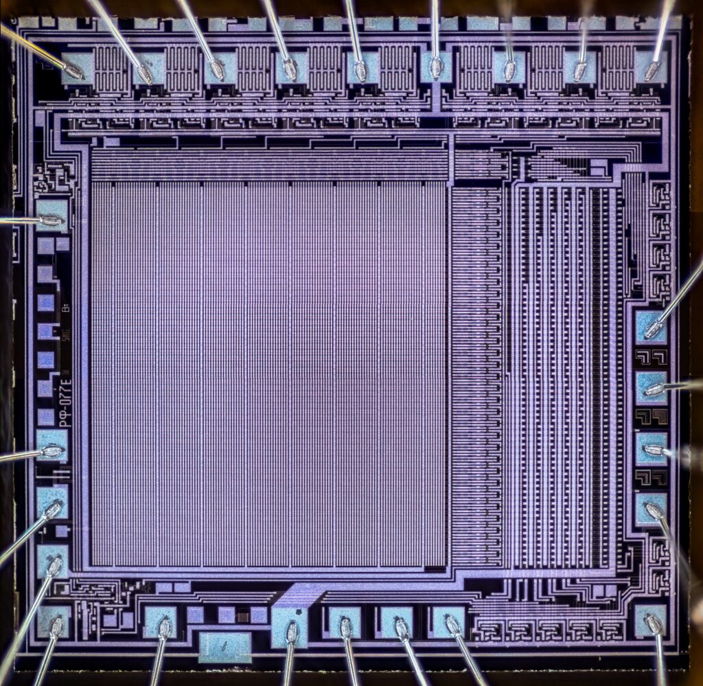
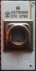
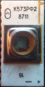
The K573RF2 die is very different from the K573RF1 die. Now it has a single field of memory cells.
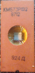
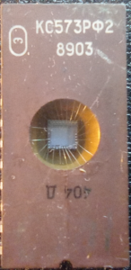
By the end of the eighties, 573RF2 microcircuits appeared in ceramic packages in terracotta shades. The package consists of two halves connected by a glass like compound. This was the same as standard western ceramic DIPs of the time, just with different compounds resulting in much different colors.
 |
 |
 |
 |
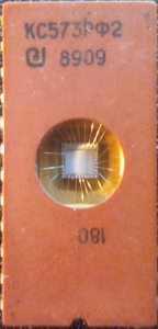 |
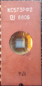
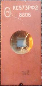
Together with the advent of these packages, a change of marking begins. Initially, microcircuits had the letter M in their name ( KM573RF2). After some time, the letter M was replaced by the letter S (Russian C).
 |
 |
 |
 |
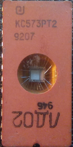
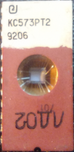
These chips are marked KS573RT2. Unusually, the letter combination RT refers to one-time programmable memory chips. Other companies, including Intel, National Semi. and Mostek, also resorted to painting over part of the surface of the microcircuit with subsequent re-marking, Basically converting EPROMs to OTP-PROMs. Intel did this a lot for their Dev boards.
 |
 |
 |
K573RF2, not KM, not KS. The thing is that the top of microcircuit is made of brown ceramics, and the bottom is made of white. The oddity lies in the fact that the resulting «sandwich» has the State Quality Mark. Clearly they were using left over parts. One wonders what the different materials did for heat cycles.
Well, the last chip of this series. In plastic package. The window for erasing is quite small. The Soviet’s were the only ones I know of that managed to make a plastic package EPROM. Finding suitable materials that would pass UV light, AND be thermally compatible is tricky.
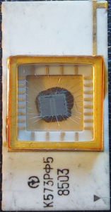
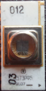
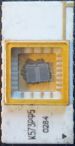
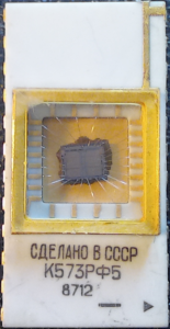
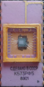
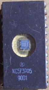
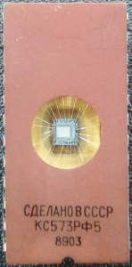
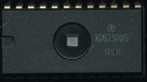
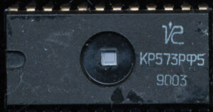
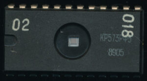
K573RF5
Microcircuits of this series are fully compatible with microcircuits of RF2 series. They were made in other factories. All chips in ceramic packages were manufactured at the Kvazar factory in Kyiv.
 |
 |
Some of the chips was made without the factory logo.
 |
 |
 |
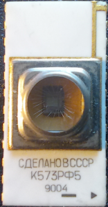 |
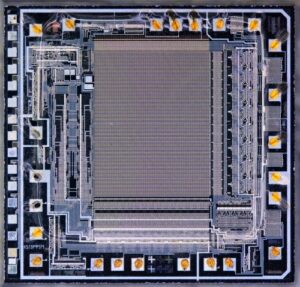
Until 1988, there was a die, divided into two memory blocks (made in 2 different sizes). After that, a die with a completely different topology was installed.
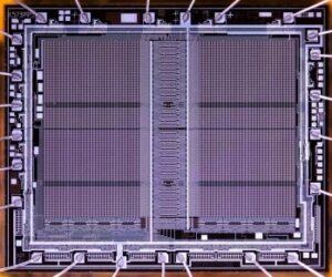 |
 |
At the end of the eighties, there was a transition to another type of package, similar to RF2 packages.
 |
 |
573RF5 microcircuits were also produced in plastic packages. Another manufacturer has been added to the Kvazar factory. KVADR factory, Chernihiv region, Ukraine.
 Kvazar |
 KVADR |
 No Logo |
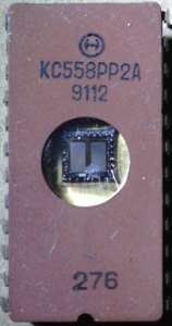
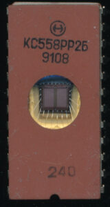
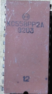
I want to finish this article with a curious fact. These are KC558RR2A/B EEPROMs. These are Electrically Erasable parts, not UV Erasable. It was also produced in a package with a quartz window. But the die was painted over with brown lacquer. It’s impossible to erase it with ultraviolet light. Socialist economy had the planned nature. Maybe the factory was behind schedule on chip production. And this was the solution.
 |
 |
 |
We’ll discuss more SOviet EPROMs in Part 2 of the article, such beauties as the RF3 , 4 6 and 8 series
I express my gratitude to Andrey Perfiliev (Andrey_cpu) and Victor Fyodorov (Victor_F) for their assistance
in writing this article.
The pictures of the dies from the site radiopicture.listbb.ru
Photos of chips are partially taken from the site 155la3.ru, as well as from the Andrey Perfiliev and John Culver (The CPU Shack) collections.
Written by: Vladimir Yakovlev
Edited by: John Culver (CPU Shack)
References:
1. www.jmargolin.com/patents/eprom.htm
2. 155la3.ru
February 27th, 2023 at 5:06 am
Memories! Wowsers I have not seen any of these since my first full time job. We were making Loran C receivers and used the Intel 4004 CPU and the 1702 eproms. Circa 1976.