Archive for March, 2021

March 23rd, 2021 ~ by admin

CPU of the Day: National Elentari x86 and What Lies Beyond – Part 2

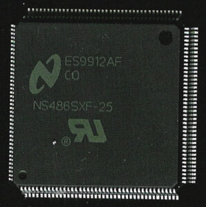
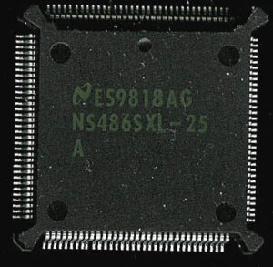
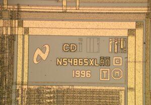
Last week we talked about a little known, but not unheard of 486 built by National Semiconductor called the NS486 Elentari.  As interesting as a non-Intel x86 architecture is, thats not what led me down the aforementioned rabbit hole.  This is what did…

The entrance to the Rabbit hole lay in an issue of Boot Magazine.

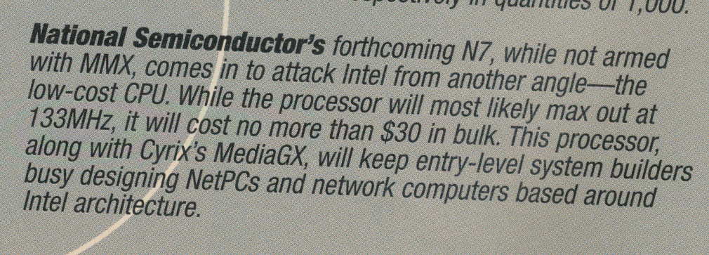
This small blurb in Boot magazine from back in August of 1997 is all it took.  What was this mysterious N7 processor that even Boot Magazine felt the need to mention?  It is being compared to the Cyrix MediaGX, which coincidently National had agreed to merge with right about the time this issue went to press, a fact that may or may not have been known to the authors at the time.  Regardless, the deal wasn’t officially completed until 1998, so that meant this mysterious N7 had been in development for some time, and probably had reached something a bit more then a glitter in an engineers eyes….and indeed it had.

Mentions of the ‘N7’ in the press at the time start in early 1996 and continue through 1997, this indicates that the N7 was likely planned soon after the beginnings of the NS486 core.  Its very likely that the NS486 was to be a stepping stone to the bigger more powerful N7.  The N7 is described as a 133MHz ‘Pentium compatible’ processor.  The NS586 core (as it was called by National) was an enhanced NS486, with the pipeline extended to 5-stages and using Nationals new 0.35u process, just as some had originally suggested for the NS486.  This resulted in a 3.3V processor running at 133MHz.

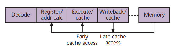
NS586 5-Stage Pipeline – Cache could happen on Stage 3 or 4 and Memory Access was non-blocking (image (c) MPR)

The NS586 was planned to be at least 2, and most likely 3 different processors (in similar fashion to the NS486SXF and NS486SXL).  The common core to all of the designs was the 5-stage NS586.  This took the NS486 and greatly enhanced it, adding 8 of L1 cache (4K Instruction + 4K Data). The pre-fetch buffer is doubled in size to 32-bytes as well as some Out of Order execution support.  The decode and memory/cache access logic is also further optimized.  Cache accesses can be shifted between the 3rf and 4th stages as needed, allowing modifying, loading or storing of cache data in two consecutive cycles.  Unlike the K6 or PII the NS586 does not use intermediate instructions in executing x86 code, it directly executes each x86 instruction (like the NS486 before it).  The updated pipeline executes all code as fast or faster then a 486 and in some cases faster then a Pentium.  National claimed that the 133MHz core would perform as a Pentium 95, compared to say a AMD 5×86-133 being rated at a Pentium 75 level. As with the NS486 before it, it lacked an onchip FPU.

The NS586 core was not exactly small, even on the 0.35u process it took 930,000 transistors (426,000 of which is the cache).  This resulted in a die size of around 25.8mm2. (roughly the same size as the core only NS486 on 0.65u).  And it was intended to be even bigger…

Lise the NS486 before it, the NS586 was to be integrated with a variety of peripherals, and this time National was going big on the integration.   At the top was the N7-Lite, which integrated the NS586 core with a SVGA 2D graphics controller, TI TMS320C50 based DSP and Audio controller.  This in addition to a PCI bus, DMA controller USB, IrDA, and other normal peripherals of the era.  The N7-Lite does not have a traditional DRAM controller, instead using a controller geared towards a UMA (Unified Memory Architecture) to use the system RAM for the CPU and the onboard GPU. The GPU is designed to support only a TV out (NTSC PAL and SECAM outputs) as this was to be a full NetworkPC on a chip, basically what became Set-Top Boxes of the 1990’s.

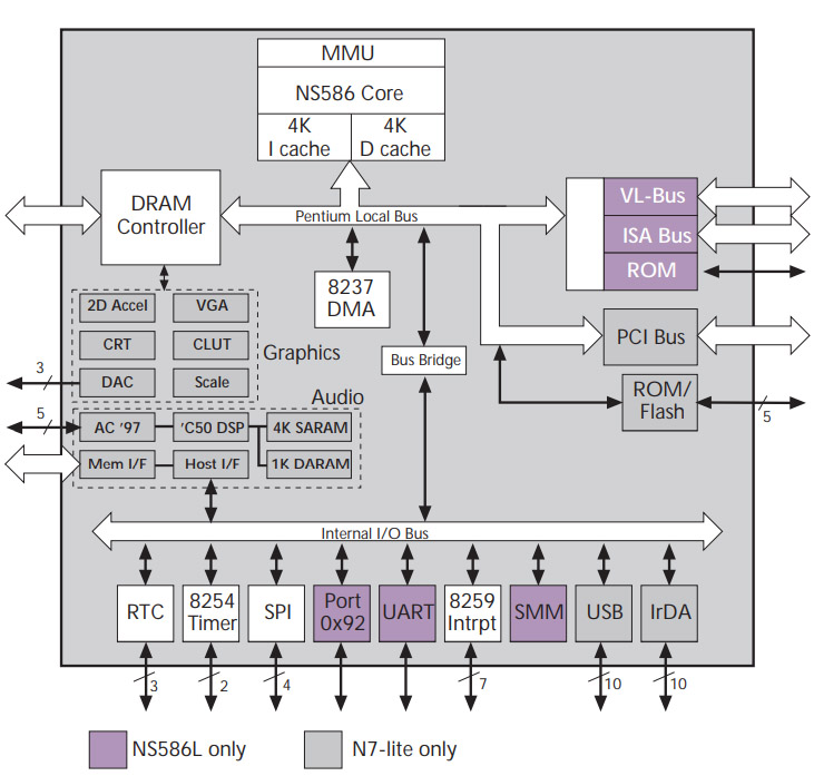
NS586L and N7-Lite shared the same core but with different peripherals as well as busses (image (c) MPR)

On the low end was the NS586L, which dropped the audio, video, and PCI bus and added a standard Pentium compatible VL-Bus, ISA, and DRAM/ROM controller, this is more of a enhanced NS486 with a similar set of peripherals, and likely would be the logical successor to designs using the 486.  Speed was to be 100MHz (again to differentiate it from the N7-Lite) and estimated cost was to be $25/chip.  Pricing for the N7-Lite was not announced. It’s unknown how far these designs progressed, whether actual silicon was made or not.  Having a transistors count and die size was indication they were pretty far along, perhaps having the chips floor plan finalized and working on taping it out for masks (6 months seems reasonable for samples after tape out).

Both of these chips were scheduled (as of October of 1997) to begin sampling in the second quarter of 1998.  Its very likely that a third chip was planned, if only due to the naming of the ‘N7-Lite.’ ‘Lite’ indicates that it is something less then the full version, and the Boot blurb (as well as some other press mentions) only refers to the ‘N7.’  In all likelihood there was to be a top end version known simply as the N7.  Such a chip would likely replace the TV only GPU in the N7-Lite with something that supports standard CRTs or LCD panels, perhaps more RAM support and Ethernet and/or an EIDE hard drive controller (something that the competing Cyrix derived ST STPC included).  We may never know, as despite the efforts of the engineering team the project was inevitably canceled in favor of the newly acquired MediaGX line from Cyrix.  This line continued to be developed at National even after they sold the rest of Cyrix off to VIA (eventually selling the MediaGX division to AMD).

Sadly they didn’t

Perhaps someone who worked in the Arador group at National can offer more insight, but until then we can only speculate of what could have been another interesting processor on the x86 scene in the 1990’s.

Posted in:
Uncategorized

March 18th, 2021 ~ by admin

CPU of the Day: National Elentari x86 and What Lies Beyond – Part 1

National Semi NS486SXF-25 Rev C0 -1999

While I was casually reading an issue of ‘Boot’ Magazine from 1997 I was sent down the rabbit hole by a mention of a processor in a small blurb in a footnote of an article.  Just a few lines really is all, but about a processor I was not familiar with, an x86 one at that! So nearly a month later, I have emerged from the rabbit hole.  We will begin not with what sent me to the hole in the first place, but when and where the hole itself came from, and that is the year 1995, the place? National Semiconductor.

As mentioned in the 486 Overclocking article, the 1990’s were a boon for up and coming x86 processors.  In some ways it was similar to the processor bonanza of the 1970’s but centered on x86.  Many companies wanted to have a go at the x86 architecture market.  National Semiconductor was of course interested in making something with x86 as well.  They rightly decided that a head to head competition with Intel for mainstream PC processors wasn’t the best idea, but that embedded computing, low cost set top box (as they later would become) and ‘Network PC’s’ would be a good market.  The goal was to design a simple efficient x86 processor and integrate it with many peripherals, and sell it for $20-30 each.

Elentari Core. 16-byte Prefetch Buffer, 1K Cache ,16-bit Data Bus and support for 2 8M DRAM Pages


NS486SXF/L Block Diagram (SXL omits blocks in dashed lines)

The core project began in very early 1995 (or late 1994) and was known as the Elantari, Queen of the Stars in Lord of the Rings Mythology.  The Elantari (aka the ESF94001) had three priorities in its development (in order): 1) Schedule, 2) Low Cost, 3) Performance.  Time to market was essential, even at the expense of performance optimization. The core (which the Marketing dept quickly renamed to the NS486) was to be a 486 compatible core (using protected mode only) with some optimizations and was organized officially under a new unit at National Semiconductor called the Arador Unit (someone really liked LotR). Target speed was 25MHz at 5V on Nationals 0.65u process using a very simple 3-stage pipeline (Fetch/Decode, Execute, Write Back).

NS486SXL-25 No Rev Marked 1996 (courtesy xSecret)

Balancing cost and performance meant that die area should be minimized, as this effects yields and parts per wafer.  This, on a 0.65u process, allowed for a small area of cache.  National ended up, after a fair amount of analysis, going with a 1K direct mapped instruction cache (that can bus snoop) and a 16 byte prefetch buffer.  This is in great contrast to the Intel 486 which had a 8KB unified cache (and 16K on later 486s).  But for embedded use instructions have a better performance increase when cached then data.  Cache also presents some difficulties with real time computing, as its difficult to know how long an operation will take if you don’t also know whether it s from cache or the main memory.  National provided a method on the NS486 to load and lock the cache with a set of instructions that would ALWAYS operate out of cache.  This combined with assigning one DRAM page to Data, and another for stack use, made timing more predictable and consistent when needed.  As part of the development process National used IP they had licensed from another IIT, whom had earlier designed a 486 class processor. IITs IP was not used in the NS486 itself, but was used in helping debug, design and develop it and its testing environment.

NS486SXL-25 Rev A – SXL unique die – 1998

The NS486 core lacked both a FPU and MMU, and had a 16-bit data bus.  This allowed for a fairly small core size.  The core alone took up about 256,000 transistors (roughly half of what the Intel 486 integer core used) and on the initial 0.65u 3-layer process results in a core die size of 29.6mm2 including the cache. (the SXL die with limited peripherals pushed that to around 64mm2)  The short pipeline greatly restricts the speed, it never made it above 25MHz (though 33MHz was apparently achievable.

National Semiconductor by this time had become dominate in integrated peripheral chips, led by its ‘SuperIO’ chip line, and it was this integration that made the NS486 unique.  National designed two versions of the NS486, the NS486SXF with a full set of peripherals, and the smaller NS486SXL with a few less.  The integration of peripherals was one of the most challenging aspects, the core itself is relatively simple, but adding other features, often with different clock and signal domains is much harder to design and test.  This is where National’s expertise on SuperIO chips came in handy.

The other challenging aspect of a x86 design in the 1990’s was from the legal department.  Intel claimed that even a clean design of anything x86 ‘MUST’ violate at least one Intel patent.  National however had designed the NS486 from the ground up, including the microcode, AND as a backup, also possessed a license from Intel dating back to the 1970’s (it was that license that helped lead to the National/Cyrix merger).

  NS486SXF NS486SXL
Package 160PQFP 132PQFP
Cost $25 $15
486 Core
X
X
DRAM Controller
X
X
DMA Controller
X

LCD Controller
X

ISA Bus Interface
X
X
External Bus Master Controller

X
UART/IrDA
X
X
ECP Parallel Port
X

PCMCIA Controller
X

Real-Time Clock, Timers
X
X
Programmable Interrupt
X
X
Reconfigurable I/O
X
X
Programmable Chip Select
X
X
3-Wire Serial Peripheral
X
X

NS486SXL Rev A0 die – matches package markings – Still 0.65u (courtesy aberco)

Initially both the NS486SXL and SXF used the same die, with the SXL having some of the onchip features disabled. National planned on making a seperate die later for the SXL to further reduce costs.  They did this in around 1998.  Their goal was also to shrink the design to their upcoming 0.35u process but it is unknown if they successfully did this (dies from 1998 continue to be of the 0.65u variety).

Initial samples were available by early 1996, a rather quick development.  The NS486 was well supported in both hardware and software.  It supported a number of common real-time operating systems of the time, including pSOS+, QNX, VxWorks, and VRTX. It did not however support DOS, having no real mode support. In 1997 the NS486SXF was used to implement Jav Nanokernel, a Java based OS running the Java VM directly on hardware. Hardware vendors included PARVUS (NS486 based PC104 board), BCT (Dev Boards) and several others making ready made NS486 based SBCs.   In November of 1996 National released a full Web Browser based Network computer Reference design using the NS486 called the ‘Odin’  This was the first sub-$200 web browser capable computer of the time.

NS486SXL die – Peripherals take up about a third of the die (die photo from aberco)

In 1997 things got a bit more interesting.  National Semiconductor decided to merge (in all reality it was an acquisition) with Cyrix.  The NS486 continued to be made, but by 1999 National listed it as ‘not recommended for new designs’  It would also appear that some things never really got finished.  Datasheets up through at least Dec of 1997 were still ‘Preliminary’ though the silicon had been produced for sometime.  Production of the NS486 continued well into the 2000s, with chips being made at least into 2003 and probably later.

The NS486 Performance in integer tasks was pretty good. In some cases beating the Intel 486DX. THis is largely because of its optimized instruction timing, many are single cycle, much faster then other cores.

At the time of its introduction it had little competition (in the x86 realm).  Intel had the 386EX and AMD had an the 386SC (what later became the ElanSC300 line).  Both of these were 386 class parts that were slower (and in the case of the 386EX) more expensive.  Intel themselves did not have a good embedded 486 option largely due to lack of trailing edge fab capacity.  Most of their fabs had been (or were being) converted to higher end processes to make new Pentiums and P6 chips, while their older fabs were filled to the brim with Intel’s then booming chipset business.

ARM 610 Motorola 68349 Hitachi SH7032 NEC V820 MIPS LR33020 Intel i960CA AMD 386SC Intel 386EX NS486SXF
Frequency 20 MHz 25 MHz 20 MHz 25 MHz 25 MHz 25 MHz  25 MHz  25 MHz 25MHz
Dhrystone MIPS 18 9 16 18 14 30 5.4 7.1 12
FPU No No No Yes No No No No No
MMU No No No No No No Yes No No
Cache None 1K Inst None 1K Inst 4K/4K 1K Inst None None 1K Inst
Periphs. Some Some Some Some Some Some Full Set Some Full Set
Transistors 359k 550k 593k 380k 700k 600k 335k ?? 500k*
Process 1.0u 0.8u 0.8u 0.8u 0.7u 1.0u 0.7u 0.8u 0.65u
Price $20 $33 $30 $80 $67 $90 $49 $33 $25

*Estimated Core = 256k Cache = ~50k

It was suggested that if National lengthened the pipeline of the NS486 to the then standard 5-stages, and moved it to their new 0.35u process that it could ‘easily’ hit 133MHz at 3.3V.  But what embedded designer would want to have to deal with that fast of a processor?  It would seem that the NS486 team had ideas beyond just the purely embedded market, as something more then the NS486 was their ultimate goal, and exactly what led me down this Rabbit hole……

In Part 2 we’ll look at what National developed from the NS486, and if it wasn’t for the MediaGX they acquired, very likely would have made it to market.

Posted in:
CPU of the Day

March 10th, 2021 ~ by admin

The Story of the Soviet 8080 Processor – The 580

Before beginning the history of the Soviet 580 series microprocessor, we need to say a little bit about the level of Soviet computing technology before the advent of integrated microprocessors. This is really a topic for a separate article, so just two facts.

This article is largely from guest author Vladimir Yakovlev, translated from Russian, and edited/expanded by me.  It is part of a series on Soviet microprocessors that started with the Soviet T34 Z80 article. 

In 1950 the “Small Electronic Computing Machine” (SECM) was made in the USSR. It should be noted that in the USSR this computer was launched at a time when there was only a few computers in Europe, the English EDSAK, launched just a year earlier and Zuse’s Z4 in Zurich in ~1947. But the processor of SECM was much more powerful by parallelizing the computational process.

In the creation of the SECM, all fundamental principles of computer creation were used, such as the presence of input and output devices, the encoding and storage of the program in memory, the automatic execution of the computation based on the stored program, etc. Most importantly, it was a computer based on binary logic used and currently used in computational engineering (the American ENIAC used a decimal system (!!!)).

In 1975, during the historic Soyuz-Apollo space mission, the control was carried out by the complex, which included the BECM-6 (Big Electronic Computing Machine), a direct descendant of SECM. This system allowed for one minute of flight computation time, while on the American side of the flight it took 30 minutes of computation.

BECM-6 (Science Museum, London)

The real tragedy was the decision to produce IBM-360 clones in the USSR, that is, the transition to copying American architecture. I mean, obviously, whoever’s copying doesn’t have a chance to outrun (THe the USSR regularly added enhancements to Western designs). Copying has only one meaning – as a stage of learning. When you don’t have your own technology. Today, China is demonstrating the effectiveness of this approach. But the logical end of such an approach is still a shift to proprietary developments.

From that moment on, the Soviet Union was catching up.

At the end of 1962, by the decision of the Government of the USSR, the Kiev Design Bureau was established in Kiev, later the Kiev Institute of Microdevices (KNIIMP), with an experienced plant. It was KNIIMP that was chosen to copy Intel’s products. The first task was to create a copy of the i8080 and was started in August 1976, just 2 years after Intel introduced the 8080 to the Western World.

In 1977-1978, the first prototype chips were completed. The first basic set of the series contained three chips, K580IK80 (8080 CPU), K580IK51 (8251 USART) and K580IK55 (8255 PIO Controller).

They were produced in 48-lead metal-ceramic planar package. Contrary to popular belief, it is not a layer-by-layer copy of the Intel 8080 (some blocks are similar, but the layout and location of the bonding pads are significantly different). On November 6, 1980, the New York Times published an article “Soviet Gaining in Computers”.  in which the author of article also reached this conclusion.  These ran at 2MHz (500,000 ops/ec) and were made on a 6 micron NMOS process.

In 1981-1982 the package were replaced with the standard (Soviet pin spacing) DIP. Both versions for the domestic economy in plastic cases and for special applications in metal ceramics were released.

580VM80 – 1988 – Military spec

Around 1983, the names were changed from IK80 to VM80, IK55 and IK51 to VV55 and VV51 respectively. The additional letter “A” denotes an upgraded version of the processor from the extended base set of the series. In this variant, the speed was increased to 2.5MHz 625,000 op/s, the area of the die was reduced by 20%, (resulting from a process shrink to 5 microns) and the periphery of the crystal was redesigned.

KR580IK80A – 2.5MHz – 1982 – “KWAZAR” (KIEV, UKRAINE)

The 580 series was produced by many of the Soviet IC design houses, for many years.  Including, Kvazar, Electronpribor, Rodon, Kvator and Dnepr.


KR580IK80A “ELECTRONPRIBOR” (FRYAZINO, RUSSIA)
( “O” – pre-production sample)

“KVANTOR” (ZBARAGH, UKRAINE)

“RODON” (IVANO-FRANKIVSK, UKRAINE)
Top package is a early (1983) ‘Chocolate’ Brown PDIP

Late Production (1991) KR580VM80A – “DNEPR” (KHERSON, UKRAINE)

Chips manufactured for export were marked with the inscription Сделано в СССР and didn’t have the logo of the manufacturer.  The ‘manufacturer’ was the USSR, as that was more important then which state enterprise it came from, as a matter of national pride.

Export version (for Export to other Soviet Aligned countries)

In a sense, reproduction of microcircuit analogues is akin to a very high quality translation of foreign literature into native language. It is necessary not only to completely transfer the purpose of the product itself, but also to make it technologically compatible for the domestic producer. This is a very difficult task.

While the 8080 and 8086 microprocessors were at issue, the KNIIMP was successfully performing its task. But once Intel developed and started the 80286 and then the 80386, the Soviet Union was unable to produce similar microprocessors.

It can be argued that Intel Vice President Robert Noyce’s suggestion has been fully realized – the Soviet Union had fallen behind the United States in the development and production of modern microprocessor circuits forever.  Even to this day Russia continues to make variants of Western processors, from the MCS-96 series, to Microchip PIC17’s.  It should be noted that they did make a myriad of somewhat custom microcontrollers for specific tasks, that did not have direct Western Analogs (though sometimes they claimed these devices to be analogs of chips that they were not, in order to meet the direction of ‘copy the West’)


Posted in:
CPU of the Day