Archive for the 'EPROM of the Day' Category

January 19th, 2023 ~ by admin

A history of the EPROM in the Soviet Union
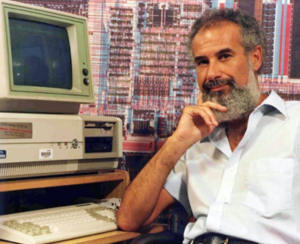
Dov Frohman

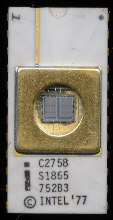
In 1971 Intel came out with the first memory that could be not only programmed by the user, but could be erased with UV light and programmed again. This was the 1701 EPROM (quickly revised into the 1702 EPROM and 1702A). It was 2048 bits (256×8), used PMOS, and required three voltage (+5V, +12V and -12V) to operate, and each data line required a strobed -48V pulse for programming.

The 1701 was introduced to the world in the May 10, 1971 issue of Electronics Magazine in an article written by Dov Frohman, the inventor of the EPROM.  Today Intel is more known for, and remembered by their microprocessors, but until the early 1980’s it was EPROM’s that carried the company.  They accounted for the largest share of profits at Intel for over a decade.
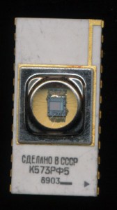
K505RR1

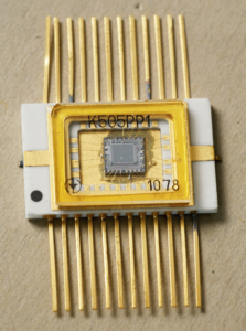
Soviet K505RR1 – 1978

Intel 1701 – Unmarked


The first EPROM chip produced in the Soviet Union was the K505RR1, developed by the Kyiv Research Institute of Microdevices and manufactured by the Kvazar factory in Kyiv, Ukraine. The chip is a 2048-bit (256×8) electrically programmable read-only memory with ultraviolet erasure. It is an analogue of the 1702А.
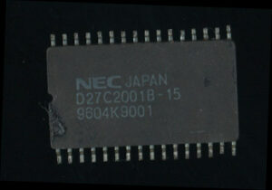
They supported up to 20 (they wore out quite quickly)  overwrite cycles and had a data retention period in on state of not less 5000 hours. This is one of the only EPROM chips manufactured in the flat pack package. NEC made a 2Mbit flat pack EPROM in the 1990s, quite a strange beast.
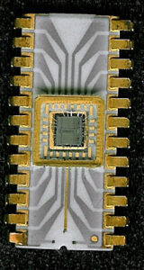
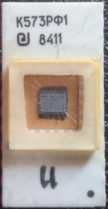
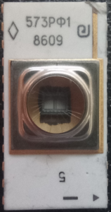
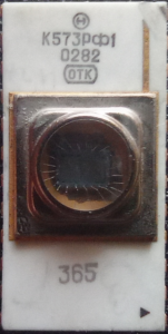
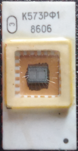
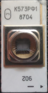
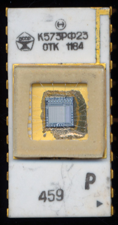
K573RF1

Analogue of the i2708. The microcircuit is a read-only memory device with a capacity of 8 Kbit (1024х8). Supply voltages of  12v, 5v, -5v. Data Retention period in on state is not less 15000 hours. Number of write cycles at least 100. (a nice improvement over the previous generation)

Microcircuits were manufactured at two factories: Novosibirsk Factory Vostok and Novosibirsk Electrovakuum Factory (NEVZ). The ‘3’ logo is an export version.

NEVZ – 1984


NEVZ military grade version(without letter K + rhombus) -1986

Vostok – 1982


Export – 1986


Export – 1987


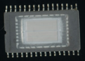
On microcircuits with a metal cover, you can see that a part of the conductor connecting this cover and GND pin has been mechanically removed. In electrochemical coating, it’s necessary that all surfaces on which gold is deposited in this case be connected to each other.  But the K573RF1 chip has three power supplies. And minus 5 volts is applied to the die substrate. Part of the conductor has been removed to avoid a possible short circuit.

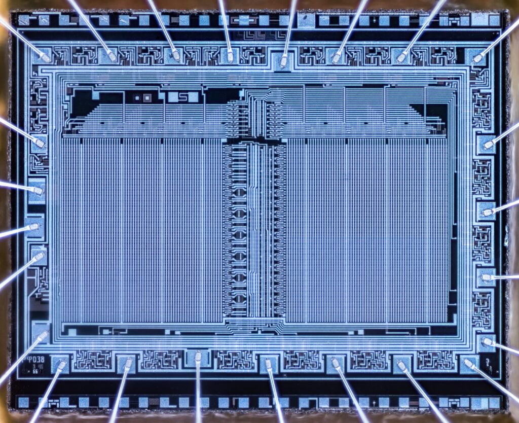
It’s clearly seen that the die of K573RF1 is divided into two memory blocks.

In the manufacture of dies, it happens that several memory cells turn out to be damaged. The manufacturer blocks access to damaged part of the die by connecting one or two input addresses to ground or a power supply. Either guarantees the operation of only half of the data bus of the microcircuit. K573RF11, K573RF12 have an information capacity of 4 Kbit (512×8) ,  K573RF13, K573RF14- 4 Kbit (1024×4).

Read More »

Posted in:
EPROM of the Day

November 22nd, 2016 ~ by admin

More EPROM Die Fun

National 2758 - Intel 2758 (1979) - Intel 2758 (1980)

National 2758 – Intel 2758 (1979) – Intel 2758 (1980) – Click for larger version

Recently I got in some nice 2758 EPROMs.  The 2758 was a 5V 8k EPROM and really the first of the standard EPROMs (with industry standard pinouts, voltages, etc).  The original 2708 required 3 supplies (5V, -5V and 12V) while the 2758 required only +5VDC.  EPROMs are particularly nice as due to the fact that they need a window to allow UV light in for erasure, you can also have a clear shot of the die (in most cases).

Two things caught my eye on these 3 EPROM’s.  First, the National Semiconductor 2758 die looked suspiciously like the Intel die.  This isn’t too unusual as National was one of Intel’s primary second sources throughout the 1970’s.  Intel did not have the best fab’s early on so second sourcing was a must.  As a product of this some strange things happened, such as Intel die’s being in National labeled parts (though the reverse is not known to have happened).

Intel 2758 w/ 2716 die

Intel 2758 w/ 2716 die

The second thing you can see in the picture is the difference in die structure between the otherwise seemingly same Intel 2758’s.  One has bonding wires on all 4 sides, while the second one has bonding wires only on the top and bottom of the die, and a completely different layout to the die.  My first suspicion was that the Intel and National may both be the same die, so I put them on my scanner (I REALLY need  a microscope). At 4800dpi (or 9600dpi on one) you can see that they are in fact different dies, and both are not 2758 dies….

National 2758 also using a 2716 die

National 2758 also using a 2716 die

Both are actual 2716 dies! We saw this several years ago with 2708s being used as 2704’s as well as in Soviet designs.  The third die is a 2716 die as well.  All Intel (and National) did was leave one address line unused (tied to ground in this case).  Its likely these dies had a defect so the affected area was effectively disabled by not using that address line.


C2758 S1865 - Defective 2716 die using only the upper 8k

C2758 S1865 – Defective 2716 die using only the upper 8k

The difference in the Intel dies is also interesting.  Early in the production of the 2716 Intel changed the die layout to increase density. That’s why one die has the bonding wires on all 4 sides and the newer die only on top and bottom (which made assembly faster and more reliable

as well as increasing density).  The 2716 was released BEFORE the 2758, the 2758 being almost an afterthought, it is very likely that ALL 2758 dies are actually 2716 dies, as it would make little sense for Intel to create a separate mask set for a product that was likely to be low volume.  The 2758 data sheet lists pin 19 as AR (Address reference) and specifies it to be driven low, or for the S1865 driven high.  Pin 19 on a 2716 is A10 so AR on the 2758 is simply selecting the lower 8k or for the S1865 the upper 8k.  Being as there was 2 versions of the 2758 using different parts of the die, its clear Intel was using defective 2716 die to make the 2758, at least early on.  Later documentation simply has Pin 19 listed as GND.

As a side note, the CPU Shack REALLY needs a microscope, sorry for the blurry photos from the scanner.

Tags:
,

Posted in:
EPROM of the Day

April 22nd, 2014 ~ by admin

Soviet K573RF23 and the Mark of Quality

Soviet Vostok K573RF23 - 2kx4 - 1984

Soviet Vostok K573RF23 – 2kx4 – 1984

This EPROM, made in November of 1984 at the Soviet Vostok factory in Novosibirsk started life as a 2716 2kx8 EPROM.  A Soviet 2716 would be marked as 573RF2, whereas this particular example is marked 573RF23.  The die is a 2716 that was found to be defective, and thus converted to a  2kx4 EPROM, this is denoted by the adding of the 3 to the part number.  This certainly was not an uncommon procedure, even Intel regularly sold 2708 EPROMs as 2704s, whether to use a die with an imperfection, or to simply meet demand.

There are two other interesting markings on this particular EPROM.  First is the CCCP logo, this is the State Quality Mark of the USSR.  This quality mark was used to signify that products met the following conditions:

  • “meets or exceeds the quality of the best international analogs”,
  • parameters of quality are stable,
  • goods fully satisfy Soviet state standards,
  • goods are compatible with international standards,
  • production of goods is economically effective and
  • they satisfy the demands of the state economy and the population.

Meeting these conditions allowed the factory to sell such devices at a 10% premium.  So not only was Vostok able to pass a defective part as a quality part, they were able to do so and make a bit extra revenue.  Thats something Intel would be quite envious of.

Some references show that 573RF23 as being the equivalent of a 2758 EPROM (5V 2708).  This is in fact incorrect.  A 2716 converted to a 2708 is done so simply by removing a single address line (going from 11 to 10)  The 573RF23 retains 11 address lines, but it removes 4 data lines, thus making it 2kx4, same number of address locations, but each locations contains only 4 bits, vs 8 bits.  Rewiring address lines likely did not allow for a working EPROM due to where the defect was, thus cutting the word size down.  The first condition of the State Quality Mark is that said EPROM should meet or exceed the best international analog.  Intel did not make a 2kx4 EPROM, the closest western analog would be the Harris/Intersil IM6657, though it was made in CMOS, vs the 573RF23s NMOS, so one could say that it was easy to beat a analog that did not exist.

The other mark on this EPROM is OTK, which literally means “Technical Control Department,” in others words this part passed the quality control dept, hopefully after it was converted to the lower capacity device, and them marked with the State Quality Mark.  Perhaps it was the best NMOS 2kx4 EPROM the world was to see, certainly it came in a beautiful package.

Tags:
,

Posted in:
EPROM of the Day

January 7th, 2013 ~ by admin

2012: Year in Review: UV EPROMs

Unusual double marked Intel HC2708. Intel used 'H' for a brief time to denote a windowed DIP package.

Unusual double marked Intel HC2708. Intel used ‘H’ for a brief time to denote a windowed DIP package.

UV-EPROMs are a technology made obsolete in an incredibly short period of time by widely available, and more flexible, Flash and EEPROM technology.  Processors evolved, DRAM and SRAM evolved, EPROMs simple ceased to exist.  There were attempts to make them faster, lower-power, or in more convenient packages, but at the end of the day (or the end of the 90’s) shining a UV light into a small round window to erase them simply became a sign of an era long passed.  That window, however, also allows for the beauty and in some cases massiveness, of their silicon dies to be seen by all, something today’s black plastic flash simply cannot do.

Here are a few of the interesting EPROMs I found in 2012 (click to enlarge)


AMIS5204A-7604

AMI made many custom chips for clients, as well as second sourced various designs.  This is a S5204A, a copy of the National Semiconductor MM5204.  Made in 1976 it stored 4kbits and had a ‘fast’ access time of only 750ns.  It could be fully programmed in ‘less then a minute’ and took ‘only’ 10 minutes to erase all 4096 bits.  Power draw was 750mW max, about the same as a 800MHz Intel Atom processor.

AtmelAT27C256R-55LC_600dpi

The Atmel AT27C256R-55LC was a CMOS 55ns 256kbit EPROM in a surface mount package.  Made in late 1996 it was the beginning of the end for EPROMs.

IntelC27C202-70V05-ES

Intel used some unusual packages for a few of their EPROMs.  This package was more commonly used on things like C8751s.  Here it is a C27C202-70V05 Engineering Sample.  This is a 2Mbit EPROM.

SovietK573RF5-8903

No EPROM collection is complete without at least a few examples of Soviet EPROMs.  If anything for their amazing packages.  Here a Soviet of unknown plant K573RF5 made in 1989.  This is a clone of the Intel 2716.

TITMX2532-35NL

The Soviet bloc mastered making EPROMs with plastic packages, but this never caught on in the western market.  I have never seen a production EPROM in a plastic package out side of East German/USSR.  However I did acquire a plastic TI TMX2532-35NL.  TMX denotes it as a prototype.

WSI27C256L-15-5962-8606305XA

The military and industrial markets continued to use EPROMs far longer then the commercial/consumer markets.  Cost being less of a concern then reliability.  EPROM’s had a proven track record and thus were used until Flash had proven itself.  This is a Waferscale Integration (WSi) 27C256L-15 mil spec EPROM.

Tags:
, ,

Posted in:
EPROM of the Day

September 27th, 2012 ~ by admin

EPROM of the Day: AMD AM27C2048 – Shrinking Dies

AMD AM27C2048-150DC – 3 Dies (Click to view larger)

In the semiconductor industry process shrinks are highly sought after.  They result in smaller die sizes for the same part, which results in more chips per wafer, thus increasing revenue.  There are other benefits (typically speed increases and power decreases (aside from leakage)) but from a purely economical stand point, the smaller dies result in more profits.

Rarely do you get to SEE the result of these process changes.  UV-EPROMs fortunately have a window, for erasing them with UV light, that also lets the die be seen.  Here are three AMD AM27C2048 EPROMs.  These are CMOS 2-Mbit EPROM, pretty common in the 1990s.  As you can see that while they are all the same part, the dies are significantly different. While its hard to say for sure without a die analysis, we can make some good estimations based on what foundries AMD had at the time these devices were made.  The first EPROM is date late 1993 which will likely be a 1 micron process.  The second EPROM, dated mid 1997 is a bit smaller, around 20% smaller, which fits with AMD’s 0.8 micron fabs.  The last, and latest, EPROM was made in 1998, likely at the joint AMD-Fujitsu (FASL) plant in Japan.  This would mean it is a 0.5 micron device. The plant was transitioning to 0.35 micron at the time, but that was most likely used for the higher profit Flash memory devices.  By 1998 EPROM’s were on the decline.

Also of note is the different copyrights.  The first two are copyright 1989 while the third is 1997.  Its hard to know for sure (I do not have the microscopes/tools needed to do die analysis) but it is likely the 1 micron to 0.8 micron was an optical shrink. Literally this means that the die (and masks) are scaled down to a new smaller process with no architectural changes.  This is simple and inexpensive.  Sometimes changes will have to be made to support a new process, or make full use of its benefits, so a new layout/masks are made.  This is likely the case with the 1997 copyrighted EPROM.  The design was altered to work with the new, smaller process, and it was significant enough to warrant a new copyright.

Tags:
,

Posted in:
EPROM of the Day

September 16th, 2012 ~ by admin

EPROM of the Day: Plastic MME U552D – Intel 1702 Clone

MME U552D – Plastic 1702

Today’s EPROM is a very rare early prototype from MME (VEB MikroElektronik “Karl Marx” Erfurt ).  Part of the East German state-owned electronics business.  MME (and their predecessor FWE) made clones of Intel 1702, 2708-2764 EPROMs as well as many processors.  These were all unlicensed, reverse engineered, or copied via industrial espionage since this was all before the end of the USSR, and the technology blockade put in place to ‘prevent’ Eastern Europe from using Western technologies.  This particular U552D is a clone of an Intel 1702A, however, it is made in a plastic package (with what appears to be a actual quartz window).   A very unusual package that was used in Soviet devices mainly and very rarely in the west.

The only western EPROM I have found in plastic is a prototype TMX2532-35NL from Texas Instruments (thus the TMX prefix).


However, the MME U552D actually has the window glued to the top of the plastic package, rather then integrated into it like the TI, and the Soviet designs.

Tags:
,

Posted in:
EPROM of the Day

April 29th, 2011 ~ by admin

EPROM of the Day: Intel D87C75PF The 8755 gets a boost

Intel C8755A - 1977

When Intel released the 8755 in 1976 and 8755A in 1977 it provided an easy way to interface the 8080 and the 8085 to other components. It was a 16k (2kx8) EPROM with a pair of latched 8 bit I/O ports.  This greatly reduced system chip counts and complexity of board design. The basic 8755A ran at 3Mhz (the later 8755A-2 ran at 5MHz) which allowed interfacing with the 8085AH with zero wait states. The 8755A continued to be used well into the 1980s with many processors (Intel and others)

Intel D87C75PF - 1988 Engineering Sample

By 1988 the 8755A was out of date, its 16k of EPROM space was insufficient for most designs and its power consumption was much higher then contemporary parts. Intel sought to remedy this with the release of the 87C75.  The 87C75 is essnetially a 27C256 EPROM, and 82C55A port expander, and latches combined on a single chip. It was made on Intel CHMOSII-E process which reduced power consumption (from 1.5Watts to 500mW). It ran at a max of 5MHz and the EPROM was bumped up from 16k to 256k. It was designed to interface direction to the 8051, MCS-96 and i188 processors.

Why then do we find so few examples of the 87C75PF?  The late 80’s and early 90’s also ushered in dozens of microcontrollers and embedded processors that had all of the 87C75’s features on chip; larger EPROM on die, more I/O ports, and the widespread use of Flash on microcontrollers effectively made the 87C75PF obsolete.

June 8th, 2010 ~ by admin

Unlocking EPROM cores?

Its well known that manufacturers such as Intel and AMD will sell quad cores as dual cores, or 6-cores as quad-cores in order to meet demand, or to use dies that didn’t ‘make the cut.’ This process has been going on for over 30 years though. Back in the 70’s and 80’s it was very common for a device such as this:

Intel D2704 4k EPROM

Which is a 2704 4k EPROM, to actually be made from a 2708 die, just with not all the leads connected, or sometimes, with them connected but just labeled as the smaller part. In a production environment, it is cheaper to have a single production line making dies that can be used in more then one device, then having an entire seperate production line just to make a product that may not be the most popular.  Look at this die shot (its a bit blurry) but you can see its a 2708 die.

2704 with 2708 die

Once again, whats new, really isn’t we have just went from small EPROMs, to CPUs with billions of transistors

November 9th, 2009 ~ by admin

EPROM of the Day: ST M27C160

As EPROM capacities increased due to insatiable demand for more storage, die sizes increased rapidly as process shrinks could not keep pace. This is the result.

ST M27C160-150F1

ST M27C160-150F1

This is a 16Mbit EPROM from ST from around 1995. Today we have Flash, and in the same space can store Gigabytes of data.

Posted in:
EPROM of the Day

April 8th, 2009 ~ by admin

EPROM of the day: Intel MC1702A/C – Miltary Antique

Intel who we know as a CPU company, actually got its start, and most of its revenue, by making EPROM’s (Electrically Programmable Read Only Memory).  EPROM’s were actually Intel’s most profitable product line through 1985.


Intel MC1702A/C EPROM

Intel MC1702A/C EPROM

The 1702A was introduced in late 1972, it holds all of 256bytes. (2048 bits). This particular device is MIL-STD-883 Class C compliant (Class C no longer is used today).  It had to undergo much more testing and process control then a regular commercial device, as well as work in higher/lower temperatures.  This particular part was made in late 1976. Sadly it has a couple missing pins, but for being 32 years old is not bad.

Posted in:
EPROM of the Day