
The 486 CPU Era – The Birth of Overclocking. – Part 1
Introduction
486 CPU Era – the birth of Overclocking – this is how I decided to call everything that was in the pre-Pentium era, which I did not find and become familiar with until a couple of months ago.
(Another Article in cooperation with max1024 of Belarus – Edited/Expanded by Me)
 If we abstract from the very first Pentiums, which appeared using Socket 4 in two speeds of 60 and 66 MHz, then these processors won popular fame and love in motherboards based on Socket 5 and 7. Such machines could be seen in the early 90s on which while playing C&C, Warcraft and other RTS games. The Sega Mega Drive II and Super Nintendo game consoles competed with expensive computers. Moreover, the consoles were far ahead in popularity (and to be honest, the graphics and game play were better) and I got used to the joystick much earlier than to the mouse and keyboard.
The question arises, what was there before all these Pentiums? And the answer, if you dig deeper, can discourage or even confuse any inveterate computer enthusiast, since the cultural layer of “hardware” from the very first processor belonging to the x86 architecture to the first representatives of the superscalar architecture is much larger than from the Pentium 4 to the freshly released Intel Core i9-11900K, which belongs to the Rocket Lake family of 11th generation Intel Core processors. It is not so easy to digest this entire historical layer, so I have outlined the framework for myself.
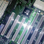 To simplify the chosen concept, I decided that the platform should in any case support the PCI interface, since it is, firstly, relatively fashionable and “modern” and, secondly, gives more room for my experiments with the accumulated PCI expansion cards. I did not impose other, special requirements on the test platform, except that according to the established tradition, it should be the most powerful and fastest set that is possible to assemble.
Here I think some of the readers of this article the “True oldies” will say: “what is this nonsense, where is the ISA, VLB and 8-bit only?”, But everything has its time, we will gradually dive into the depths of the prehistoric hardware sea, otherwise decompression cannot be avoided. [Editor’s note, I grew up on an 8-bit 8088 and of course connected the PC Speaker to a 100 Watt Stereo Amp, the loudest 8-bit beeps ever]
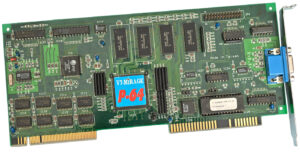
typical VLB videocard – V7 Mirage P64 on S3 Vision 864, 2 Mb (before they hid all the good stuff with a heatsink)
So, let’s play from the presence of the PCI bus, which appeared just during the heyday of 4th generation processors, “fours” or simply – four hundred and eighty-sixths, which first appeared back in 1989 or today it is 32 years ago. “Almost like yesterday” the oldies will say, “We were not born yet,” the rest will answer, although this is not the point.
 The previous generation of 386 processors was content to exchange data with peripheral devices more often at the “width” of 8 and 16 bits, although the entire generation of processors belongs to the first microprocessor architecture supporting 32 bits, but despite this, motherboards designed for them had no 32-bit PCI bus. Although this could not have happened historically, since the specification is new, in relation to the previous buses, it (PCI) was first implemented in 1992. This means that the whole choice comes down to the whole variety of 486 processors, and there was enough variety in those years, not that today there is a choice between “red” and “blue”.
Species diversity
Charles Darwin “Each species is fertile enough for the surviving offspring to multiply, to ensure the growth of the population”
 In his landmark and world-famous work “The Origin of Species by Natural Selection”, Charles Darwin devoted a special role to species diversity and natural selection. If his theory of the origin of species is empirically correlated with the struggle for survival in the processor market, then we can conclude that Evolution has already ended and only two subspecies remain on the highest pedestal of the food chain – “red” and “blue”. And we just have to be unwitting witnesses of the Revolution, when finally one species completely engulfs or annihilates the other and reigns … I think we don’t need such happiness =) However, Charles Darwin’s theory remained a theory.
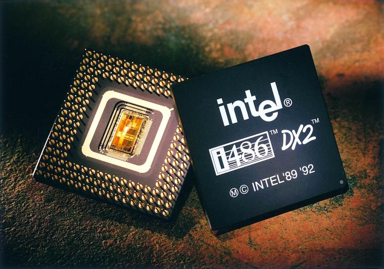
Returning to the species diversity of all 486 processors, I want to note that they were produced at different times by as many as seven manufacturers who produced not one processor model, but even several parallel lines for various tasks with different processor models. Modern users only dream of such a variety, there is not much to choose, and this is precisely the result of evolution and natural [and unnatural selection in the case of Intel suing several out of existence] selection. Before getting to know the representatives of processors from different manufacturers, I will start with an advertising kit from Intel, designed specifically for their 486 processors.
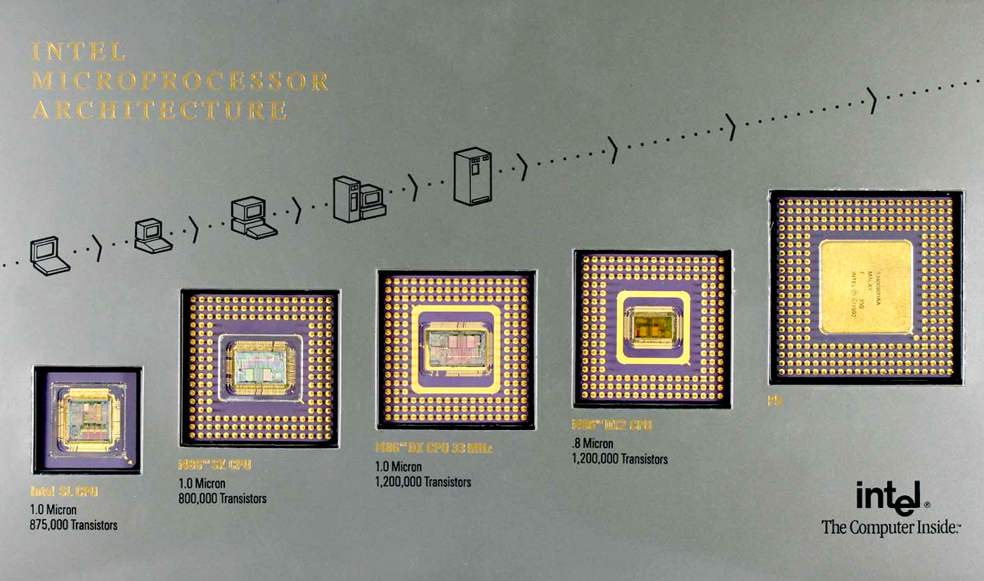
Before you is a masterpiece of art, more correctly – an advertising product released in 1992, which tells about the outstanding microprocessors released by Intel.
 The first exhibit is a processor from the 386 family – Intel 80386SL. It is a mobile microprocessor with a 386 core and power-saving features not found in the desktop 386. This processor has an unusual design for x86 microprocessors – the land grid array (LGA), most were in a Plastic QFP. Interestingly, the 80386SL had over 800,000 transistors – three times as many as the desktop 386SX / DX (integrating many chipset features onto the die).
The second processor belongs to the 80486 family – Intel 80486SX. The first 486 processor without FPU. The product ad claims the i486SX has 800,000 transistors, although this is contradicted by other Intel sources. According to them, the i486SX processors had about 1.2 million transistors for 1 micron chips and 0.9 million transistors for 0.8 micron chips. Conclusion – no one is immune from errors, even inside the CPU, though they may have deducted the transistors that were used by the disabled FPU.

80486-25 Pre-DX SX249
The third exhibit is the DX version of the i80486 processor. The difference between DX and SX processors is that DX chips have a working built-in module for calculating floating point operations, while SX does not (it was disabled in early chips, and removed in later versions completely). The die of this chip is the same size as the SX die- approximately 16 mm x 10 mm, that is, 160 mm2.
The Intel Pentium 60 microprocessor closes the evolutionary branch of development. This microprocessor is an early production version with the FDIV error, which was in the floating point unit in the original Pentium processors manufactured by Intel in 1994. The error was expressed in the fact that when performing division on floating point numbers using the FDIV processor instruction, in some cases the result could be incorrect.
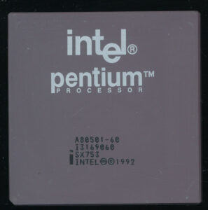
Early 1993 Pentium 60 – With the FDIV bug (and overheating problems later fixed by moving to a huge heatspreader package)
Intel knew about the problem, but preferred not to expand on it. They believed that since this defect is significant only for a narrow circle of users (mathematicians and other scientists), then users who want to replace the processor should contact the company and prove that it is they who need this replacement. (Charles Darwin would say about this in our time that if you need a modern video card, then you must first prove that you cannot play modern games without ray tracing the best one with an acceptable FPS for you =))
Intel had had many bugs in their processors before (early 486s and early 386s were VERY buggy, some 386s so much so that they were limited to 16-bit code, the FDIV error though became a bit of a media sensation. Perhaps a sign that computers had finally become mainstream enough that a bug could generate that level of attention.
And then I will briefly talk about those seven manufacturers of 486 processors, the models of which I will test below and even try to overclock them =)
Intel
Let’s start with Intel. In the fall of 1989, at the Comdex Fall computer show, held in Las Vegas, Nevada, USA, Intel presented its new fourth-generation 32-bit x86-compatible microprocessors built on a hybrid CISC-RISC core. They received the name Intel 486 or i486 for short. The frequency range of processors started at 16 MHz and ended at 100 MHz. The entire 486 CPU line was divided into two camps, with and without an integrated floating point unit (FPU). The first type of processors received the suffix “DX”, and the second “SX”. It should be noted that initially the FPU was embodied in silicon, but if a defect was found in this block during the production of processors, with the remaining processor blocks fully functional, the processor was simply turned into the “SX” version, or some kind of “Celeron” these days. The very first production of 486s (in 1989) did not make this distinction, it was simply the 80486, no DX to be found, the DX was added at the turn of the decade, in 1990.
Early processor models had 8 KB of unified L1 cache for code and data. In later versions of the CPU, the cache size has been increased to 16 KB. The early i486 models worked with the cache on the Write Through principle (WT for short), but later learned to work with the cache using the Write Back (WB) function. When using this more productive principle of working with data, if there was a copy of the data in the cache, the information was written only to the cache memory, writing to the RAM was not performed, while with the pass-through write, the data was always written to the RAM, even if they were already present in cache.
classic 486 set – external L2 cache with a 1 MB capacity)
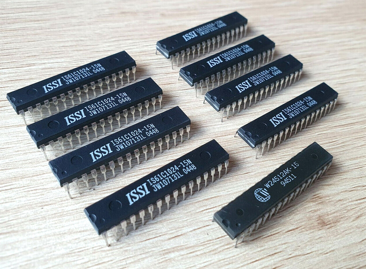
The i486 processors did not have a second-level cache; instead, an external cache was located on the motherboard (it worked at the CPU bus frequency), the volume of which could be increased with your own hands by adding more capacious memory chips to special sockets, or simply increasing their number, if, of course, the motherboard had this function. Some motherboards has a special slot for a cache module called a COAST (Cache On A STick) to simplify this. The L2 cache size was measured in kilobytes and in the maximum configuration could reach 1024KB.
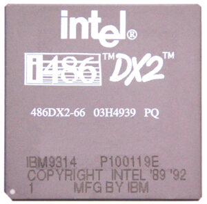
 Speaking of the i486 processors on this overclocking resource, it is worth noting that it was this generation of processors that gave the whole world such a concept as – Overclocking, in its full understanding, since it was in the i486 that the first multipliers of the base frequency or simply multipliers appeared. Previously overclocking required clock crystals on the motherboard to be replaced. The i486DX2 processors had a multiplier of x2, and the lineup consisted of models with frequencies from 40 to 66 MHz. The manufacturer’s assortment included the only model i486SX2 processor with a frequency of 50 MHz. The i486DX4 processors had a x3 multiplier, although the name of the model itself hints at a x4 multiplier. These models included processors with a frequency of 75 and 100 MHz.
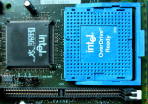
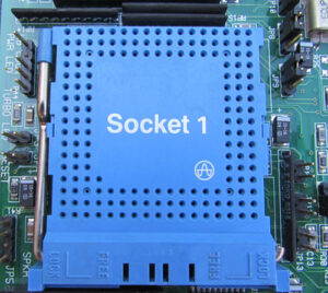 During the 486s, there was also a fashion for Upgrade processors, and even Intel itself encouraged this activity and even released a separate line of Intel 486 OverDrive processors. These processors were intended (initially) to be installed in a special Socket, which was designed to install the i487SX mathematical coprocessor, which, in fact, was an ordinary i486DX, but with a different sequence of contacts (CPU legs). Often on motherboards one could find a soldered i486SX and a second socket for installing a mathematical coprocessor i487SX or OverDrive, or even two sockets, one of which was made of blue plastic and had the inscription “Intel OverDrive ready” or just a blue socket without designations.
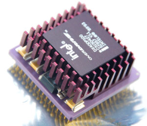
Ordinary 486 processors had 168 pins, special “Overdrives” designed to replace CPUs soldered on motherboards had one more pin – 169. An additional pin served as a kind of key for installing such a solution into the socket, and also had a shutdown function the processor soldered on the motherboard.
 When an i487SX or OverDrive was installed in the second socket, the first soldered i486SX or any other processor installed in the socket was automatically completely disabled and the second processor intended for the upgrade was already engaged in all the calculations.
After Intel introduced the 486 OverDrive processors in 1992, they used a convoluted model numbering system. Each CPU was labeled the same as the CPU it was supposed to replace. If, for example, you had an i486SX-25 MHz, then you had to buy an OverDrive labeled ODP486SX-25. Such an upgrade system was misleading and later Intel abandoned it, starting to mark OverDrive processors with their real frequency. This is because the first OverDrive processors worked at double the clock speed with built-in coprocessors, that is, they were i486DX2 processors. So the ODP486SX-25 was actually an i486DX2-50.
The popularity of these i486 OverDrive processors was great. The main advantages of the Intel 486 OverDrive processors were as follows:
• OverDrive processors contained built-in voltage regulators
• Supported write-back (WB) cache
• had a non-removable radiator and were able to operate without forced air cooling
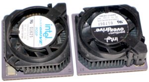
To extend the lifespan of the 486 platform, Intel in February 1995 releases a special version of the processor – Intel Pentium OverDrive with a frequency of 63 MHz. The 83 MHz version was released only 8 months later, when the age of 486 machines was rapidly approaching its end. The processor itself is a real Pentium core! Modified to interact with the i486 bus. Its bus was 32-bit, which is half the size of a full-fledged Pentium, but to compensate for the processor, the L1 cache size was doubled.
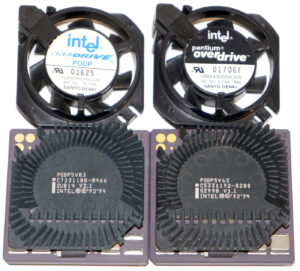
The processor is rated at 3.3 volts with an onboard voltage regulator providing 5 volts from the motherboard. The fan built into the CPU heatsink is powered directly from the CPU chassis.
AMD
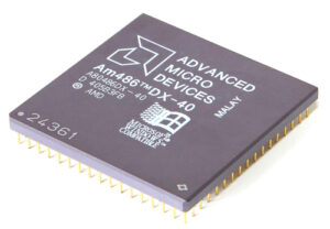 The main competitor to Intel in those days was AMD. Processors of the Am486 family were functional analogs of the competitor’s processors and initially used the same microcode of the Intel 80386 processor and the Intel 80287 math coprocessor.
Later, some models used their own microcode. In April 1993, the first processors with the Am486DX and Am486SX markings were born, similar to Intel models. DX and SX processors worked at the system bus frequency, the frequencies corresponded to similar Intel models, but the cost was 20% or more percent less. These original AMD processors also used Intel microcode, and are nearly impossible to distinguish from their Intel brethren.
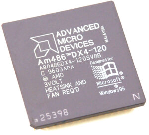
 A little later, a year later, there were models with multipliers, as well as with write-back cache. The frequencies of the Am486DX2 models were in the range from 50 to 80 MHz, and the Am486DX4 from 75 to 120 MHz, which by 20 MHz in clock frequency exceeded the TOP of the line i486DX4-100 from Intel.
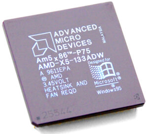
But AMD did not stop there and in 1995 released the following processor models called Am5x86. The processor die was manufactured using a 350-nm process technology and had 1.6 million transistors. The L1 cache was doubled to 16 KB, and the multiplier was 4. The processor was running at 33 MHz FSB, and thanks to the x4 multiplier, the resulting core clock speed was an impressive 133 MHz. In terms of performance, the Am5x86 was comparable to a Pentium processor with a frequency of 75 MHz, which was clearly indicated on the processor marking in the form of the inscription “Am5x86-P75”, while the processor model itself looked like AMD Am486DX5-133ADW/Y/Z.
 These processors overclocked well and easily turned into the Pentium 90 equivalent when running at 160 MHz (40 x4). Not a large percentage of processors could even work at 200 MHz (50 x4). It is believed that processors with a “Z” at the end are more successful overclocking, since according to the manufacturer’s specification they have an operating temperature of 85 C, versus 55 C with a marking ending in “W” or 75C for the “Y”. Another popular saying says that the later the processor is released, the higher the chance of it working at 200 MHz. I have personally met processors made in 1996, 1997 and 1998, but even now they are more often found from 1996.
Although the Am5x86-P75 processor is labeled with the number “5”, which should symbolize the 5th generation of processors, in fact, this processor belonged to the fourth, such a marketing move from AMD.
IBM
 “Blue giant” or IBM stood at the origins of all computer History, it is not for nothing that the slogan “IBM compatible PC” already meant that buying such a computer you will receive a hardware platform compatible with a large number of software products. Until the mid-80s of the last century, IBM felt very confident in the PC market, but when a new market player appeared – Compaq, which in 1985 released its first 80386 Deskpro 386 computer, the situation for IBM changed dramatically. To increase the share of its PCs sold in the computer market, IBM entered into contracts for the supply of processors with Intel, and then with AMD. Additionally, IBM at its manufacturing facilities produced Intel processors, the 486 version of which looked like this:
The lineup of Intel clones consisted of 33, 50 and 66 MHz models. If the bare processor was a regular version of Intel i486DX and apart from the marking on the case “MFG (manufactured) BY IBM” did not stand out, then the version with a heatsink immediately catches the eye, thanks to its unusual blue color and the name “BLUE LIGHTNING”. The BLUE LIGHTNING name was borrowed from another line of QFP only 486 processors that IBM had designed and made inhouse. The PGA versions are NOT related to the earlier QFP BL, BL2 and BL3 x86 processors.
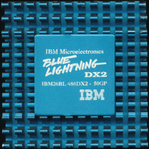
IBM Blue Lightning – Cyrix Based Version
When IBM’s contract with INTEL ended, the Blue Giant signed a new one with Cyrix and subsequent IBM processors were already clones of another American processor manufacturer (Cyrix). IBM models from Cyrix ranged from 50 to 100 MHz. The difference between the same model from Cyrix and IBM was that the IBM manufacturing facility had stricter quality control as well as tolerances [for their own marked chips], resulting in better die quality and lower operating voltage. IBM (as well as ST and TI) manufactured dies for Cyrix as Cyrix was a fabless company.
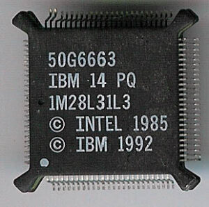
IBM 50G6663 486SLC2-66 – IBMs Own design
So if you come across an ancient IBM processor, this does not mean that it is IBM, it could be an Intel, or a Cyrix…or an IBM.
Cyrix
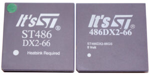
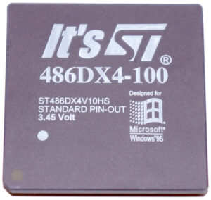
 Cyrix Corporation was an American microprocessor developer that was founded in 1988 and specialized in the supply of mathematical coprocessors for 286 and 386 processors. Cyrix was a CPU manufacturer with no manufacturing facilities of its own (fabless). For the manufacture of processors, they used the manufacturing facilities of SGS-Thomson (now ST Microelectronics), Texas Instruments and IBM (all three of which possessed x86 licenses from Intel to make such manufacturing ‘legal’) . Since 1993, Cyrix had launched its 486 processors, which include the Cx486S, Cx486DX, DX2 and DX4 models.
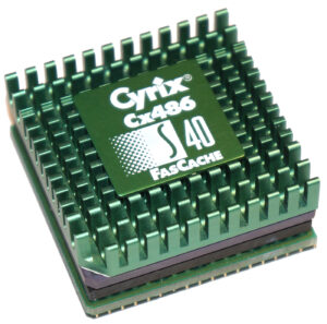
Cyrix’s first 486 processor was the Cx486S (codenamed M5). It was designed as an alternative to the Intel 486SX as it did not have an integrated floating point unit (FPU). However, the processor had a 2KB write-back cache and a special “Write-Burst” (WB) signal that gave a slight performance boost in some applications, provided the motherboard was able to use this feature. These processors were labeled “FasCache” to emphasize this feature, as most processors used slower write-through (WT) caches. Three models of such processors were released with frequencies of 25, 33 and 40 MHz.
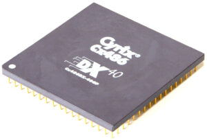 A little later, the Cyrix Cx486DX models (codenamed M6) appeared, which in their essence were Cx486S plus an internal floating point unit (FPU) and a fourfold increase in L1 (8 KB) cache size. The operating voltage for the processors was 5 V, and the lineup consisted of models with 33, 40 and 50 MHz (50MHz models were very often faked from slower ones). Despite the impressive 50 MHz, such processors were not in demand, since at such a bus frequency the peripheral devices installed with them worked extremely unstable, as were the motherboards (the same was true of Intel’s DX-50 processors).
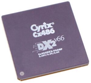 Five months, it took such a period of time to release models with doubled and tripled frequency, in relation to the release of the first 486 processor. All of these processors had 8KB internal L1 cache. Many models had writeback L1 cache (WB) and were available in 3.3V, 4V, and 5V versions (and several voltages in between, and multi voltages, the variety was mainly due to making them compatible with what motherboards could provide) . The processors were based on their own microcode and were about 5-10% slower than the real Intel 486. The processors were produced with or without proprietary green heatsinks. At this time, Cyrix processors gained popularity thanks to upgrades of old systems designed for a single 5 volt supply, since they could install the popular 66 and 80 MHz models, which were powered by Cyrix from 5 V, versus 3.3 V from competitors.
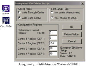
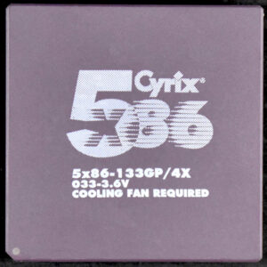
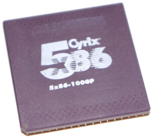 In 1995 Cyrix released its fastest and latest Socket 3 processor, the Cx5x86 (codenamed M1sc). It was no longer just a 486 processor, but something more, as it contained elements of the next fifth generation architecture (Pentium, P5). Cyrix 5×86 had a 64-bit internal and 32-bit external data bus, had a parallel operation system, branch prediction (which sometimes was enabled, and sometimes not) and optimization of instruction execution. The large 16K internal L1 cache could be configured for both write-through and write-back. Cyrix Cx5x86 processors have a voltage of 3.6 V and are designed to operate at 80, 100, 120 and 133 MHz.
However, the 133 MHz version is extremely rare and is in great demand among CPU collectors. Most CPUs can be configured to use x2 or x3 multipliers, but some models support x3 and x4 multipliers. Sometimes this can be seen in the markings on the surface of the processor or heatsink, and sometimes not. The processor also has the ability to programmatically disable multiplication, and special knowledge and utilities are required to properly configure it in different operating systems. Now everyone relies on Plug & Play, before it was much more complicated.
As a result, the Cx5x86 turned out to be a very productive processor and only had the Intel Pentium Overdrive 83 MHz and AMD Am5x86-P75 with a frequency of 133 MHz to truly compete with. But, despite the lower clock speed, the Intel Pentium Overdrive had a much more powerful coprocessor and the Cx5x86 processors lagged behind in the speed of floating point calculations (something that would ‘plague’ Cyrix CPUs for many years.
 The decline of the Cyrix Corporation as an independent structure began in the fall of 1997, when Cyrix was bought by National Semiconductor. In 1999, the combined company Cyrix National Semiconductor was acquired by the Taiwanese company VIA Technologies. National Semiconductor retained the MediaGX designs (based on the Cyrix 5×86) which then were later sold to AMD, who went on to continue making the GX line for several years. The Cyrix Cx486DX core continued to be licensed and used by other companies for nearly 20 years, including by ST, and ZF Micro.
ST – IT’s ST and Texas Instruments
For Socket 3, you can still find processors whose name is not very familiar to anyone these days and these processors have a very unusual appearance. These are all Cyrix processors manufactured by two semiconductor giants ST Microelectronics and Texas Instruments under license.
ST Microelectronics (ST) is a multinational electronics and semiconductor manufacturer headquartered in Geneva, Switzerland, formed from the merger of two semiconductor companies in 1987: SGS Microelettronica from Italy and Thomson Semiconducteurs from France. In accordance with the agreement between SGS-Thomson and Cyrix, Cyrix has granted SGS-Thomson the right to use certain microprocessors developed by Cyrix as part of SGS-Thomson’s intellectual property. SGS-Thomson was authorized to manufacture and sell such processors under its own name in unlimited quantities, with Cyrix receiving royalties from the sale of such CPUs. In addition, Cyrix is authorized to sell SGS Thomson chips under its own name.
The lineup of ST processors consisted of different models from the usual DX version with a frequency of 40 MHz to the DX4-120 model operating at 40 MHz FSB and having a x3 multiplier, as well as a processor model based on the Cyrix Cx5x86 core with a clock frequency of 120 MHz. Such processes were configured as well as Cyrix processors.
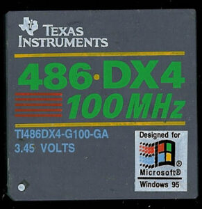
TI TI486DX4-G100-GA – Cyrix Based
Texas Instruments Incorporated (TI) is an American technology company headquartered in Dallas, Texas that develops and manufactures semiconductors and a variety of integrated circuits that are used in virtually all areas of life. The field of activity and history of this company is so vast, and the number of scientific discoveries and achievements is so great that suffice it to say that TI produced the world’s first silicon transistor in 1954, and the people from this company were later involved in the emergence of such large IT companies, like Intel.
So processors marked ST – IT’s ST are not something unusual, but the same models Cyrix Cx486S, Cx486DX, DX2 and DX4, but with some minor modifications, about which little is known. The collaboration between Cyrix and TI was shorter, and despite the fact that the development of a modified processor based on the Cx5x86 was carried out by TI, the management of TI decided to leave the processor business and the processor was never released. TI made the usual Cyrix DX2 and DX4 clones, with very colorful markings. These are identical to their Cyrix counterparts. But TI didn’t just make Cyrix clones. They had a 486 entirely of their own design as well.
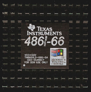
TI 486SXL2-G66-GA – TI’s own design – no FPU – odd pinout
The SXL2 is a clock doubled 486 processor without an FPU. They also had a non clock doubled SXL-40 (curiously these actually secretly support clock doubling). These had a bit different pinout and are almost always found on upgrade adapters (or special motherboards that support them)
UMC
UMC Fab
UMC is another very interesting manufacturer of the 80486 processor family. UMC or United Microelectronics Corporation is a Taiwanese microelectronics manufacturer founded back in 1980. Now UMC is one of the three world leaders in contract manufacturers of semiconductor microcircuits along with Taiwanese TSMC and American GlobalFoundries inc. I think these three manufacturers are familiar to you, because news about them appears on a regular basis in news feeds and all major manufacturers of central processors and graphics accelerators directly depend on their production capacity and the degree of mastering more subtle technical processes.
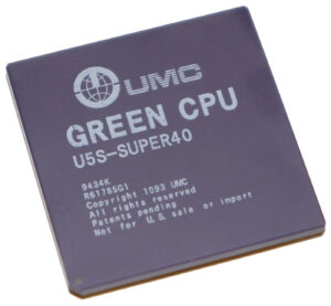 Let’s go back to 1993, when UMC presented its 486 processor called GREEN CPU. Unlike the clones from AMD that are practically indistinguishable from Intel i486 in terms of performance (and microcode), and the slower 486s from Cyrix, the UMC processor worked faster than the i486 from Intel at the same clock speed. UMC engineers revised the Intel product code and added their own developments that increased the processor’s performance. In addition to the processor, UMC also produced its own motherboard chipsets, I/O controllers, network and graphics chips, and other necessary chipsets needed to create a complete and unified computer ecosystem. And it should be noted that it was the system logic from UMC that was the fastest among all chipset manufacturers.
In 1994, Intel filed a lawsuit against UMC for infringement of its patents for their i486 processor, as a result of which the sale of UMC processors in the United States was prohibited. There is even a special inscription on UMC processors that reads: “Not for U.S. sale or import ”. As a result, the habitat of the processors fell on Eastern Europe and the countries of the former USSR. You can learn more about Intel vs the World in a previous article. In many ways it was less ‘survival of the fittest’ and more ‘survival of he who has more lawyers and money’ to the detriment of the consumer in many cases.
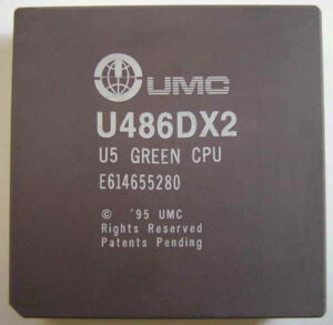 What were the UMC GREEN processors? These are processors with a frequency of 25-40 MHz, in a plastic or ceramic case. The first level cache was 8 KB, the standard voltage is 5 volts. Versions of the processor with the “SUPER” prefix worked at a reduced voltage equal to – 3.3 V. A distinctive feature of the processors was the absence of a floating point unit, but even despite this, the processor was very fast and in terms of speed at 40 MHz it could easily compete with other models manufacturers operating at 66 MHz.
Due to litigation with Intel, UMC released an analogue of the i486DX with an FPU unit, but without settling all the disputes and did not include it in the final versions of processors, which were extremely small in number. Engineering samples with the doubled frequency of the UMC486DX2 were released, but the matter did not go beyond samples. In the same 1994, Intel filed lawsuits against UMC and its distributors, UMC responded to the lawsuits with an antitrust lawsuit, and ultimately the case was settled out of court, as a result of which UMC withdrew its product and stopped production of its 80486 processors.
In Part 2 we will discuss choosing motherboards and the appropriate testing hardware, and then?! Benchmarks and some overclocking!