October 6th, 2013 ~ by admin

Decryption by an Intel 80386 – Military Style

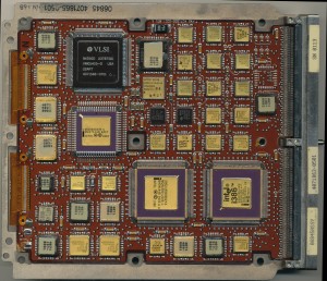
Raytheon KGV-25

Raytheon KGV-25 – Click to Enlarge

Sometimes we get processors in on boards that are just too interesting, or too good looking to remove.  That is the case with this KGV-25 correlator board.  It is a processing systems used for decrypting communications that was in wide use by the US (and likely other) militaries in the 1990’s.  The KGV-25 could receive encrypted UHF data at rates of up to 400Mbps as part of the Multi-Mission Advanced Tactical Terminal (MATT). More information on the MATT can be found here on the FAS website.

As is typical of military equipment the system did not use the latest and greatest available at the time (this board is from 1994 so the Pentium era).  The board is run by a time proven and reliable Intel 80386 processor running at 25MHz. In addition to the MQ80386-25/B (MIL-STD-883B spec 386 processor) the board contains:
Intel MQ82380-20/B  – DMA Controller for interfacing with all the assorted SRAM on the board
Intel MQ82592/B – LAN Controller for interfacing with the rest of the system
VLSI VM05403 USART – Universal Asynch/Synch Receiver Transmitter
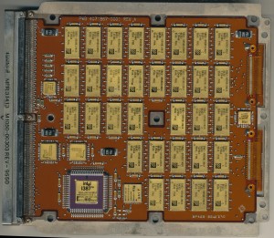
and on the back is a MQ80387-25/B Math-coprocessor for the 386 and 4MB of 35ns SRAM

Raytheon KGV-25 - Back

Essentially a complete 80386 system, of similar performance to a higher end system int he late 1980’s.  Just with a lot more gold, and built to take a lot more abuse then your average beige box of the 80’s


Posted in:
CPU of the Day

July 21st, 2013 ~ by admin

CPU of the Day: Intel Pentium Mechanical Sample

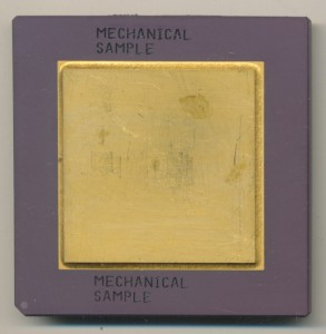
Intel Pentium Mechanical Sample - 1994

Intel Pentium Mechanical Sample – 1994

Intel and other processor companies spend a vast amount of time testing a processor design before it is released.  They want to be sure that it meets the specifications set forth in the datasheets and is free of undocumented errata.  Intel gained fame, or notoriety for the FDIV bug int he original Pentiums that caused a certain set of floating point calculations to result in an incorrect answer.  This led to the recall and replacement of many millions of processors.

Operational testing however is only one part of the testing a processor undergoes.  The package itself must also be tested.  It is tested for proper fit and function in a socket and with a variety of cooling apparatuses.  Its thermal characteristics must also be tested.  The original Pentiums were a ceramic package but quickly moved to a package with a heatspreader as they ran very hot.  In additional sample are made for testing the electrical supply of the mainboard, so that mainboard manufacturers may test their VRM (Voltage Regulation Module) design to ensure it can meet the demands of the processor.

A Mechanical Sample, like the early Socket 5 Pentium above, were used to test heatsinks, sockets, and other tasks that did not require a functioning chip.  Usually these samples did include a die (as does this one) they just are pulled from the line before final testing and speed binning.  Mechanical Samples were also used by Intel in their ‘The Journey Inside: The Computer’  education kits which typically included a processor sample, a wafer and some cut processor dies as well as some basic electronics for students to conduct experiments with.  Sometimes Mechanical Samples are devoid of marking, or like this one clearly state what they were intended for.  Some processor companies also made Marketing Samples, which were non-functioning, but often marked with color logos/graphics to advertise the processor.  Both are ivery rare to find as they were made in very limited quantities and were not widely distributed.

March 23rd, 2013 ~ by admin

Intel Pentium Processor Turns 20 Years Old

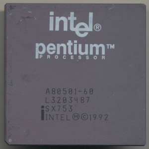
Intel Pentium 60

Intel Pentium 60 – Produced May 1993

On March 22nd, 1993 the Intel Pentium Processor was released to the public (so yah yesterday but hey whose counting). This was Intel’s first processor with an actual name.  Turns out you cannot trademark a number, so the ‘486’ name was being used by everyone (AMD, Cyrix, TI, UMC, IBM etc).  Initially known by its core name, P5, the Pentium was also the first superscaler Intel x86 processor   It had dual Integer pipelines, and a single Floating point unit allowing it to issue and complete multiple instructions per clock.

The first Pentiums ran at 60 and 66MHz and were made on a CMOS 0.8micron process with 3.2 million transistors.  After only a few months it was discovered that they ran particularly warm and the package was updated with a Copper-Tungsten heatspreader (gold plated).

A modern desktop processor such as the Core i7 Quad Core Ivy Bridge contain 1.4 Billion transistors on a 22nm process.  The P5 still lives on in the embedded market, and in the Intel Larrabee project which is itself, an updated P54C core (supporting a few more modern features such as x86-64).

Tags:
,

Posted in:
Just For Fun

March 10th, 2013 ~ by admin

CPU of the Day: Intel RUPI-44 The 8051’s lesser known cousin

Intel C8744-8 Engineering Sample - Early 1983

Intel C8744-8 Engineering Sample – Early 1983

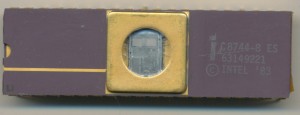
In 1980 Intel released the MCS-51 family of microcontrollers, a design that would go on to become one of the pillars of the 8-bit MCU market.  Initially the family consisted of the 8051, which included 4KBytes of on-chip ROM (or UV-EPROM in the case of the 8751) and 128 bytes of RAM as well as the 8031 which did not include the ROM, all program memory was off chip.

The 8051 was a wild success with Intel struggling to meet demand.  Intel did not have the fab capacity to produce both the 8051, and the very in demand 8088 (thanks to IBM).  In 1984 Intel opened a new fab in Albuquerque, New Mexico to build other chips, freeing up production space in the California fab for more 8051s.  Even so, an $8 8051 was routinely scalped for over $200 on the grey market and waiting periods of up to a year were common in order to receive orders, with many companies on allocation.  Intel licensed the design to both AMD (who built a fab in Austin to make it) as well as Signetics in an effort to keep up with demand.  The hardest to get part in the industry, was the 8051 from 1983-1984.

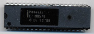
P8344 - A ROMLess 8044, so essentially an 8031 + SDLC controller.

P8344 – A ROMLess 8044, so essentially an 8031 + SDLC controller.

So in the midst of this insatiable demand for an MCU that they did not have the capacity to produce, Intel releases the RUPI-44 (Remote Universal Peripheral Interface). The RUPI-44, also known as the 8044, is an 8051 with an additional 64 bytes of RAM and a full serial communication co-processor on die.  Specifically it was an 8051 that handled the SDLC (Synchronous Data Link Control) protocol in hardware.  Intel had an SDLC controller, known as the 8273, but it was limited to 64kbps, the 8044 could handle data transfers of up to 2.4Mbps due to the 8051 core’s high speed and close coupling of the serial controller.

SDLC was developed in 1975 by IBM and was generally used as a way for mainframes to communicate with various peripherals and terminals.  It supports error correction and multi-point, point to point, and loop connections.  In 1979 SDLC was standardized as HDLC (High-Level Data Link Control) which the RUPI-44 also supports.  While popular in the 70’s and 80’s its use has faded out, though it achieved some long lived use in Europe running the Intel derived BITBUS protocol well into the 90’s.

Read More »

Posted in:
CPU of the Day

February 27th, 2013 ~ by admin

CPU of the Day: Intel 386 Double Stamp

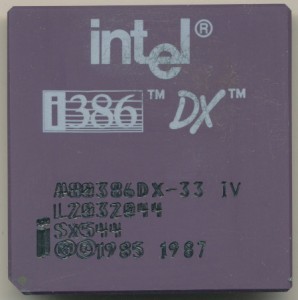
A80386DX-33-SX544DoubleMarkIn coin collecting often times an example is valued not because of its perfection, but because of its imperfections.  An off-center print, the obverse being printed upside down, or the double strike, where a coin doesn’t get cleared form the die and gets hit twice.

Such appears to be the case with this Intel A80386DX-33.  It clearly went through the engraver twice. A similar example (from the same exact lot) is fine, so clearly this one, made in early 1992, was a mistake that was not caught.  I have seen mis-aligned prints, off center etc, but this is the first example i have seen that was engraved twice.  It is interesting that even within the same lot, the spacing of the markings varied somewhat.  Notice that on the right side of the chips the sets of markings line up but they diverge towards the left.  It appears the stepper motors moving the tooling or the chips were a bit sloppy or out of calibration.

Have you seen any other double engraved comments? Let us know in the comments.

Tags:
,

Posted in:
CPU of the Day

January 12th, 2013 ~ by admin

The Intel 80186 Gets Turbocharged – VAutomation Turbo186

Original Intel 6MHz 80186 Made in 1984

Original Intel 6MHz 80186 Made in 1984

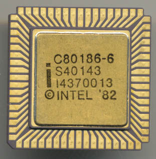
2012 marked the 30th anniversary of the introduction of the Intel 80186 and 80188 microprocessors.  These were the first, and arguably only, x86 processors designed from the beginning as embedded processors.  It included many on-chip peripherals such as a DMA channels, timers and other features previously handled by external chips.  Initially released at 6MHz, clock for clock many instructions were faster then the 8086 it was based on, due to hardware improvements.

In 1987 Intel move the 186 to a CMOS process and added more enhancement including math co-processor support, power down modes and a DRAM refresh controller.  Speeds were increased up to 25MHz (from the 10MHz max of the NMOS version).  Through the years Intel continued to developed new versions of the 186 with added features, lower voltages, and different packages.  It was not until 2007 that Intel finally stopped production of the 186 series.  It continued to be made by others under license including AMD, who made versions running up to 50MHz.  Fujitsu and Siemens also produced the 186 series. Like the 8051 the 186 gained significant support, being embedded in millions of devices.  The instruction set was familiar, debugging and development systems were (and are) plentiful so the 186 core continues to be in wide use.

As IC complexity and transistor counts increased the need for a processor core that could not just be embedded into a system, but be embedded into a custom ASIC or SoC became apparent. IC’s were being designed to handle things like DVD playback, set-top boxes, flat panel control and more.  These applications still required some sort of processor to handle them but having to have a separate IC for it was not economical.

pixelworks PW166B - 67MHz Tubro186 based Flatpanel Controller made in 2004

pixelworks PW166B – 67MHz Tubro186 based Flatpanel Controller made in 2004

VAutomation (founded in 1994) designed Verilog and VHDL synthesizable cores (meaning they could be ‘dropped’ into an IC design or FPGA).  In November 1996 VAutomation licensed the 8086/8, 80186/8 and the CMOS versions from Intel.   This gave them them ability to design their own compatible models of these processors without fear of litigation.  More importantly it allowed them to sub-license these designs to others.  In 1997 VAutomation demo’d their first 186, the V186 core.  This was a Intel 80186 compatible core that could be synthesized into a customers design.  It was ‘technology independent  which means it was not restricted to a certain process or even technology.  It could be used in CMOS, ECL, 0.35u, 1 micron, whatever the client needed.  On a 0.35u CMOS process it was capable of speeds in excess of 60MHz, and did so with less then 28,000 gates. One of the first licensees was Pixelworks, which made controllers for monitors.  Typical licensing was a $25,000 fee up front and royalties on a per device basis usually split into a high volume (over 500,000 units) and low volume.  Typical price per chip was $0.25-$2.00, which was cheaper then the $15 price Intel was charging for a discrete 80C186.

Read More »

January 7th, 2013 ~ by admin

2012: Year in Review: UV EPROMs

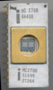
Unusual double marked Intel HC2708. Intel used 'H' for a brief time to denote a windowed DIP package.

Unusual double marked Intel HC2708. Intel used ‘H’ for a brief time to denote a windowed DIP package.

UV-EPROMs are a technology made obsolete in an incredibly short period of time by widely available, and more flexible, Flash and EEPROM technology.  Processors evolved, DRAM and SRAM evolved, EPROMs simple ceased to exist.  There were attempts to make them faster, lower-power, or in more convenient packages, but at the end of the day (or the end of the 90’s) shining a UV light into a small round window to erase them simply became a sign of an era long passed.  That window, however, also allows for the beauty and in some cases massiveness, of their silicon dies to be seen by all, something today’s black plastic flash simply cannot do.

Here are a few of the interesting EPROMs I found in 2012 (click to enlarge)


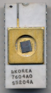
AMIS5204A-7604

AMI made many custom chips for clients, as well as second sourced various designs.  This is a S5204A, a copy of the National Semiconductor MM5204.  Made in 1976 it stored 4kbits and had a ‘fast’ access time of only 750ns.  It could be fully programmed in ‘less then a minute’ and took ‘only’ 10 minutes to erase all 4096 bits.  Power draw was 750mW max, about the same as a 800MHz Intel Atom processor.

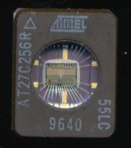
AtmelAT27C256R-55LC_600dpi

The Atmel AT27C256R-55LC was a CMOS 55ns 256kbit EPROM in a surface mount package.  Made in late 1996 it was the beginning of the end for EPROMs.

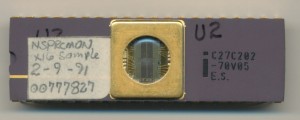
IntelC27C202-70V05-ES

Intel used some unusual packages for a few of their EPROMs.  This package was more commonly used on things like C8751s.  Here it is a C27C202-70V05 Engineering Sample.  This is a 2Mbit EPROM.

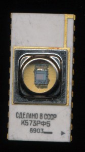
SovietK573RF5-8903

No EPROM collection is complete without at least a few examples of Soviet EPROMs.  If anything for their amazing packages.  Here a Soviet of unknown plant K573RF5 made in 1989.  This is a clone of the Intel 2716.

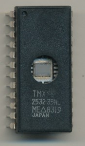
TITMX2532-35NL

The Soviet bloc mastered making EPROMs with plastic packages, but this never caught on in the western market.  I have never seen a production EPROM in a plastic package out side of East German/USSR.  However I did acquire a plastic TI TMX2532-35NL.  TMX denotes it as a prototype.

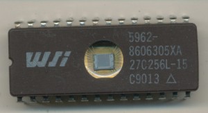
WSI27C256L-15-5962-8606305XA

The military and industrial markets continued to use EPROMs far longer then the commercial/consumer markets.  Cost being less of a concern then reliability.  EPROM’s had a proven track record and thus were used until Flash had proven itself.  This is a Waferscale Integration (WSi) 27C256L-15 mil spec EPROM.

Tags:
, ,

Posted in:
EPROM of the Day

January 5th, 2013 ~ by admin

2012: Year in Review: Processors and FPUs

Welcome to 2013!  2012, was a busy year here at the CPU Shack Museum. We added 716 new processors/EPROMs/MCUs, which works out to an average of 2 new chips per day.  This includes 16 New in Box Processors. We also added 53 new Graphics Processors, which isn’t bad for something we only collect on the side.

Some processor highlights (in no particular order, click to enlarge):

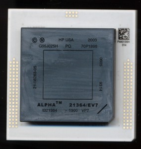
HPIB21364-1300VP7

Here is a HP/Compaq 21364 1300MHz, this was the end of the road for the DEC Alpha architecture.  It was killed off in favor of the Itanium, for better or for worse.

IBMPOWER5+19GHz

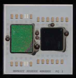
The IBM POWER5+ MCM is a stunning chip to look at, clocked at 1.9GHz its a dual core with on package L3 cache

IntelMG80387-16-SM156

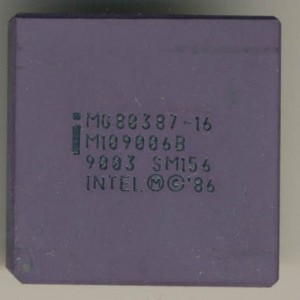
An Intel MG80387-16 SM156 US Military MIL-STD-883B spec math co processor for the 80386 processor.  Made in 1990

MME80A-CPU-9107

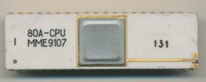
Going back in time further is this East German (MME) 80A CPU, a clone of  the Zilog Z80 made in 1991 (copied before unification, produced after, for this example).  Its always neat to see the white ceramic package, even well into the 1990’s.

NexGenNx586-P133-D-J

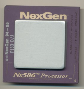
NexGen was a company that became victim of the wild processor wars of the 1990’s.  It was bought out by AMD which used its designs as the basis of the very popular and successful AMD K6.  Here is a very uncommon 133 (rated) without FPU.  Later they made a version with an integrated FPU.

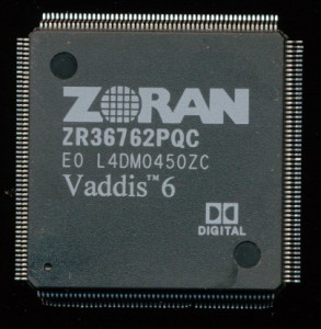
ZoranZR36762PQC-Turbo186

And to get all the way to ‘Z’ we shall go to the Zoran ZR36762.  Its a DVD controller SoC, with Dolby Digital support.  Not something one sees and thinks of as a processor.  However at its core, even in 2004, it is not an ARM, its not a MIPs, its a high speed (67MHz) Turbo186, the same 186 architecture Intel released in 1982, still being used, albeit in CMOS.

In the next few days I’ll post some EPROM highlights, then some GPU highlights.  2013 is already off to a great start with new chips coming in each week.

Tags:
, , , , ,

Posted in:
CPU of the Day

November 18th, 2012 ~ by admin

48 Cores and Beyond – Why more cores?

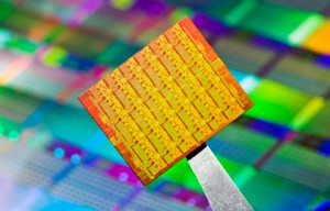
Intel 48 core Single Chip Cloud Processor

Recently two companies announced 48 core processors.  Intel announced they are working on a 48 core processor idea for smart phones and tablets. They believe it will be in use within 10 years, which is an eternity in computer terms.  Meanwhile Cavium, makers of MIPS based networking processors announced a new 64bit MIPS based 48-core networking processor.  The Octeon III, running at 2.5GHz is expected to beginning shipping soon.  Cavium already makes and ships a 32 core MIPS processor.  So clearly multi-core processors are not something we need to wait 10 years for.

Tilera, another processor company, is ramping up production of the TILE-Gx family.  This processor running at 1-1.2GHz supports from 9 to 100 cores (currently they are shipping 36 core versions).  NetLogic (now owned by Broadcom) made a 32 core MIPS64 processor and Azul Systems has been shipping a 54 core processor for several years now.  Adapteva is now shipping a custom 64 core processor (the Epiphany-IV).  This design is expected to scale to many thousands of cores.

Why is this all important?

Tilera multi-core wafer

While your personal computer, which typically is running a dual, or quad core, or perhaps even a new Intel 10 core Xeon is practical for most general computing, these processors are not adequate for many jobs.  Ramping up clock speed, the GHz wars, was long thought to be the solution to increasing performance in computing.  Just making the pipe faster and faster, and reducing the bottlenecks that fed it new instructions (memory, disk, cache, etc) was the proposed solution to needing more performance.  To a point it worked, until a wall was hit, that wall was power and thermal requirements.  With increasing clock speed processors ran hotter and began drawing immense amounts of current (some processors were pulling well over 100 amps, albeit at low voltage).  This was somewhat alleviated by process shrinks, but still, the performance, per watt, was decreasing.

Many computing tasks are repetitive, do the exact same thing to each of a set of data, and the results are not interdependent  meaning A does not have to happen before you can do B.  You can perform an operation on A, B and C, all at once and then spit out the results.  This is typically true of processing network data, processing video, audio, and many other tasks.  Coding and compiling methods had to be updated, allowing programs to run in many ‘threads’ which could be split amongst many cores (either real or virtual) on a processor, but once done, the performance gains were tremendous.
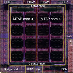
Clearspeed CSX700 192 cores @ 250MHz

This allows a processor to have increased performance, at a relatively low clock speed.  Work loads can also be balanced, a task that does not lend itself to parallelism, can be assigns to a single core, while the other cores can be busy doing other work.

There are several main benefits to multi-cores:

Increased performance for parallel tasks:  This was the original goal, split a single problem into many smaller ones, and process them all at once.  That is why massively multi-core processors began in the embedded world, dealing with digital signal processing and networking.

Dynamic Performance:  Dynamic clocking of multi-core processors has led to tremendous power savings.  Some tasks don’t need all the performance on all the cores, so a modern multi-core processor can dynamically scale the clock speed, and voltage, of each core, as needed.  If not all cores are needed, they can be put to sleep, saving power. If a non-parallel task is encountered, a single core can be dedicated to it, at an increased clock speed.

Upgradeability:  If a system is designed correctly, and the code is written/compiled well, the system does not know, or care how many cores the processor has.  This means that performance can, in general, be upgraded just by swapping out the physical silicon with one with more cores.  This is common in larger super computers, and other systems.  HP even made a custom Itanium, called the Hondo MX2 that integrated 2 Madison cores on a single Itanium module.  This allowed their Superdome servers to be upgraded with nothing more then a processor swap, much cheaper then replacing the entire server.

Not all tasks are easily handled in a parallel fashion, and for this reason clock speed is still important in some applications where B cannot happen until A is complete (data dependencies).  There are, and will continue to be systems where this is the focus, such as the IBM system Zec12 which runs at a stunning 5.5GHz.  However, as power becomes a more and more important aspect of computing, we will continue to see an ever increasing number of cores per chip in many applications. Is there a limit?  Many think not, and Intel has made a case for the use of 1000+ core processors.

Posted in:
Processor News

September 21st, 2012 ~ by admin

CPU of the Day: MicroModule Systems Pentium Gemini

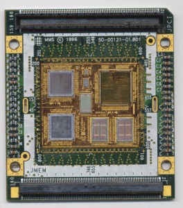
MicroModule Systems GV1-D0-3S-60-120A 120MHz (top side)

MicroModule Systems (MMS) began operations in 1992, following the completion of an agreement to acquire the assets and license rights to the technology of Digital Equipment Corporation’s MCM (Multi-chip Module) engineering and manufacturing business in Cupertino, California. The MicroModule Systems vision was to lead the next wave of electronic integration technology. Previous waves have been: discrete components (1950s), integrated circuits (1960s), large-scale integration (1980s), and system on a chip (mid 1990s).

The MMS Gemini was a module, that includes the National Semiconductor chipset die (x2) , a P54CSLM Pentium die, tag RAM, and cache RAM (128Kx2) as well as an LM75A temperature sensor for thermal management.   MMS used Intel D0 revision P54 processors (with the exception of some early C0 die), a stepping Intel never packaged themselves (it was solely used for the ‘known good die’ program).  When Intel discontinued selling fully tested dies, MMS had no way to build the Gemini and later MMX modules, so in 1998 went out of business. The Gemini was used in many mobile, and rugged PC applications such as the Motorola MW520 Computer used in many police cars.

MMS also produced MCM modules for ROSS, used to make the HyperSPARC processor as well as the Intel Pentium Pro 1MB MCM.   For a company that was only in existence for 6 years, their impact was tremendous. MMS was not alone in their production of Intel Pentium Processor modules…

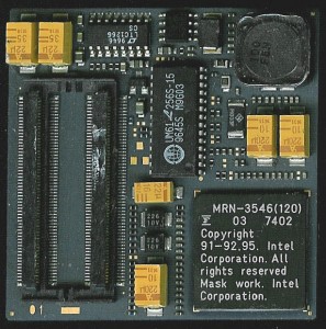
Fujitsu also made modules using Intel dies.  These were again used in rugged PC applications, laptops, and industrial computers.

Fujitsu MRN-3546 120MHz

Fujitsu made 100, 120, 133, and MMX processors on a MCM type package where the individual components are bonded/soldered to a ceramic substrate (rather then the PC Board)

Tags:
,

Posted in:
CPU of the Day