
AMD AM29501: 8-bits to the ByteSlice
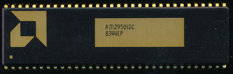
AMD AM29501DC – 10MHz Byte Slice
AMD is well known for its 2901 bit-slice processor of the 1970’s (being made well into the 1990’s), as well as the previously detailed AM29116 16-bit processor released in 1981. However, the 1980’s brought another AMD design as well, though not as complicated, it is no less interesting. In 1981, there was not a clear DSP (Digital Signal Processor) architecture, or really purpose built design. The Signetics 8X300 was well suited for such work, but was not inherently designed for it. DSP tasks were handled by other processors, or by completely custom designs. The AM29501 was not designed as a DSP, but it was marketed as a signal processor, at least for the first 5 years of manufacture. What the 29501 was, was a relatively fast, and pipelined, byte slice processor, basically a highly upgraded AM2901.
As the name suggests, the 29501 processes data 8-bits at a time, and as a slicer, it requires external program control (it lacks a PC (Program Counter) or sequencer). It has an 8-function ALU, and 6 sets of registers, which can be accessed independently, allowing for a pipelined architecture, multiple instructions may be issued before the first one is completed (as long as they don’t need the same resources). While the ALU is doing some addition, more data may be fetched, or output to one of the 3 8-bit buses. AMD designed the 29501 to be able to do advanced DSP work, and such work requires multiplication, which is something the ‘501 cannot do itself. The 29501, however, was explicitly designed to interface to the AM29516/7 16-bit multipliers. If a multiplication is needed the microprogram controller simply puts it on the multiplier bus and tells the 2951x to handle it. A fairly advanced system could be built by using a 29116 a 29516 as well as a 29501, building a complete pipelined DSP system. One of the first designs using the 29501 in such a way was a finger print recognition system, for matching images of fingerprints, a particularly intense DSP task for the 1980’s.
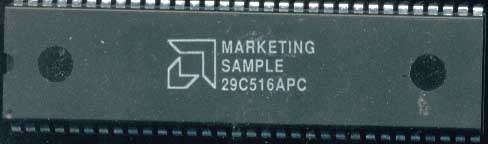
AMD 29C516APC – Marketing Sample of the CMOS 29516 multiplier, which could be mated to the 29501
When released the 29501 was a 850 gate design, made on AMD’s 2 micron (2-layer Al) IMOX bipolar process and reaching speeds of 10MHz. This resulted in a fairly small die size of 41.4mm2. A later die shrink (the 29501A) to a 1.5 micron process reduced this to 21.6mm2, though documentation does not show that this resulted in a speed increase, at lease officially. The ‘501 was packages in a rather large ceramic 64-pin DIP, with an aluminum heat spreader, owing to the heat generated by the ECL circuitry. The large package was required as the instruction input took a full 29 pins,this was not a microcoded design, the 29-bit directly manipulated drivers and MUX’s to facilitate where the data went (the 2901 was similar, though only needed 9-lines for instructions.) For example, the ALU control required 10 lines of the instruction, 4 to determine the function, and 6 to to determine where the 2 operands came from.
The 29501 enjoyed fairly wide use but was soon eclipsed by purpose built DSPs. By the late 1980’s (and with the introduction of the 29501A) AMD shifted marketing the 501 as a DSP, and more to a general processor, or parallel processor (such designs were also useful in vector operations). In 1986 LSI converted the 29501 into a megafunction for use in customers ASIC and gate array designs, named the CFA5010A. This was allowed the functionality of the 501 (and other building blocks) to be dropped into custom designs. This was later enhanced in 1990 as the CFA5012B which added some additional functionality. It is in these custom designs that the ‘501 likely enjoyed its widest success, taking only a few hundred gates, it could be added to most any array of the time.