February 14th, 2011 ~ by admin

Processor News Round-up: More cores in more places

The last week has been filled with new processor announcements, mainly for phones, but cameras as well. (yes they run some powerful processors now too).

TI is barely shipping products with its dual-core OMAP 4 applications processor and has already announced its successor, the OMAP 5.  The OMAP 5 will be a 2GHz dual core ARM Cortex-A15 (the next ARM generation after the A9). It also includes a pair of ARM Cortex-M4 processor.  the Cortex-M4 is a 150-300MHz microcontroller oriented processor.  This will allow the OMAP 5 to run basic background tasks on the slower (lower power) cores while reserving the high power cores for tasks that actually need them, increasing battery life.

Broadcom continues its drive to enter the smart phone business with the BCM28150, a 1.1GHz dual core ARM Cortex-A9 compatible with Google Android.  In December they released the BCM2157, a 500MHz dual core ARM11 processor for low-end smart phones

Samsung decided to rename the Orion processor (announced back in November) to the Exynos 4210.  A bit of a mouthful compared to Orion.

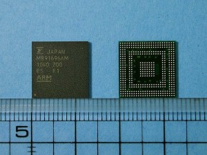
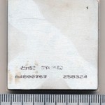
Fujitsu MB91696AM

Qualcomm showed off the  APQ8060 in HP’s new TouchPad.  This is a dual core version  Snapdragon processor we have become very familiar with. Qualcomm has an architecture license from ARM so they are free to design their own cores without having to stick to ARMs own implementations (such as Cortex-A9 etc).  This gives Qualcomm more flexibility to design in features they need, and tweak design more best efficiency.

Smart phones aren’t the only ones getting new processors.  Digital cameras now require immense amount of processing power (especially to handle 1080p video recording.  Fujitsu (yah, they still make a lot of processors) announced the Milbeaut MB91696AM.  This is a dual core ARM processor with many other DSP functions capable of handling 14Mpixel shooting at 8fps, as well as full HD video.

February 8th, 2011 ~ by admin

Qualcomm for Apple: The iPhone 4 CDMA

After years of waiting Apple has released the CDMA version of the iPhone 4.  Obviously the first carrier that comes to mind with the CDMA iPhone (and who it is being released with) is Verizon.  However, the largest CDMA carrier in the world, with over 90 million subscribers, is China Telecom.  One can imagine this is also going to be a pretty good market for Apple. The design is relatively the same as the GSM version with one major change.  The baseband processor has been changed from an Infineon X-Gold 618 to a Qualcomm MDM6600.  This is a pretty big detriment to Intel, who purchased Infineon’s wireless unit just last year. You can see the specs of the GSM iPhone 4 here, as well as all previous iPhones.

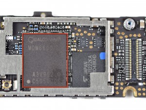
Qualcomm MDM6600 - 512MHz ARM1136 - image: iFixit

The MDM6600 (Gobi) is actually a GSM/CDMA solution, but due to antenna limitation (is anyone surprised?) it is built for CDMA only.  Once again this is an ARM powered chip.  The MDM6600 main core is a 512MHz ARM1136JS.  The X-Gold 618 of the GSM iPhone 4 runs a 416MHz ARM1176.  The ARM1136 is roughly the same as the 1176 with a few features removed.

This is good news for Apple, and certainly good news for ARM as millions of more devices with ARM processor cores will be sold.  It will be interesting to see which baseband provider Apple selects for the iPhone 5 which should support 4G.

February 5th, 2011 ~ by admin

Atmel Buys MHS, Again – The Twisted History of Atmel, Temic and MHS

Today Atmel purchased MHS Electronics, a French company.  Why is this interesting? Because this is not the first time Atmel has bought MHS, in one form or another.  Atmel, Matra, MHS, and Temic’s histories are rather intertwined, with mergers, acquisitions and name changes occurring frequently over the last 25 years.

A Bit of History….

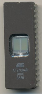
Atmel 4Mbit EPROM - 1995

Atmel was founded in 1984 by George Perlegos, a former Intel employee, as a fab-less semiconductor company.  Originally Atmel designed EPROM’s and PLDs.  They were manufactured by Sanyo, which had an Intel license.  Intel, however, sued Atmel (along with Hyundai, iCT, AAS, Cypress, and Pacesetter Electronics) over EPROM patents in 1987.  The courts sided with Intel which severely hampered Atmel’s ability to make EPROM’s.  Their focus then switched to non-volatile memories, such as Flash for which they have become very well known and continue to make.  In 1989 they bought their own fab (from Honeywell) in Colorado Springs, CO and in 1993 released an 8051 (Intel licensed) with integrated Flash memory.  This catapulted Atmel into the microcontroller market that is today one of their core businesses.  In 1994 Atmel Purchased SEEQ, an EPROM and EEPROM company that Perlegos helped start in 1981.  In 1995 Atmel opened a fab in Rousset, France, thus beginning the French connection.

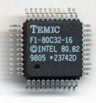
Temic 80C32 - 1998

Temic had its beginning in 1903 as Telefunken (Ironically a joint venture of Siemens and another company).  In 1967 AEG merged with Telefunken and in 1985 Daimler-Benz bought Telefunken-AEG and renamed it to simply AEG. The semiconductor division of AEG was then called TEMIC (TElefunken MICroelectronics).  In 1998 AEG sold TEMIC to Vishay, another automotive electronics supplier.  Vishay only had interest in the discrete and power electronics portions so immediately sold the IC portion to Atmel. This gave Atmel a Bipolar fab in Germany

Matra Harris Semiconductors SA (MHS) was created in 1979 as a joint venture between Matra, the French high technology group, and Harris Semiconductor, an American semiconductor manufacturer. In 1989, Harris withdrew from the partnership, and the name was changed to Matra MHS SA. Two years later, AEG (The electronics division of Daimler-Benz) purchased 50% of Matra and merged the unit with its TEMIC Semiconductor subsidiary. In 1998, AEG purchased the remaining shares of the company and the name was changed again, to MHS SA.

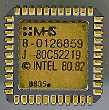
MHS 80C52 - 1988

This was part of the sale to Vishay mentioned above, which Atmel then purchased.  MHS had one CMOS fab in Nantes, France which was included in the sale

Here is where it gets complicated…

The result of all of this was Atmel now owned Temic, MHS, 2 fabs in France, one in Germany, their original fab in Colorado as well as a fab in England, and one in Texas.  Atmel needed to consolidate their fabs so in 2005 they sold the MHS fab in Nantes France to Xbybus, a French company. Xbybus ran the Nantes fab as MHS Electronics.  In 2008 Atmel sold their fab in Germany (the former TEMIC fab) to Tejas semiconductor.  This left Atmel with one fab in Colorado, and one in Rousset, France.  Labor issues at the French fab in regards to Atmel’s need to reduce production led to indefinite strikes at this fab, hampering Atmel’s work to sell it.  Finally in 2010 Atmel received approval from the French gov’t to sell the fab to LFoundry, a French company.  This marked the end of Atmel’s fab presence in France…..

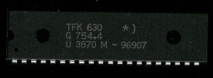
Telefunken U3870M CPU (Mostek Clone) - 1986

For about 9 months…

Today, Atmel has bought MHS Electronics, and their fab in Nantes, France, a fab they owned from 1998-2005.  MHS had been having financial troubles since 2008.  An interesting end to a series of event that began over 30 years ago.

I suspect though that we have not yet heard the last of MHS, or perhaps TEMIC.

February 2nd, 2011 ~ by admin

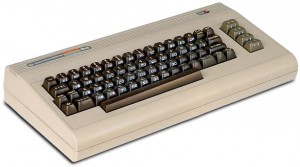
How many Commodore 64 computers were really sold?

Production numbers of vintage technology have always been a somewhat mysterious subject.  How many 4004 processors did Intel actually make? I am not even sure Intel knows.  Unlike modern car companies who can track production numbers down to the shift of the day it was made, computer companies of the 70’s and 80’s were rather fast and loose with record keeping.

Thankfully with some research, serial numbers and some math (the famous tank equation) Michael Steil of Pagetable.com came up with what appears to be a very good estimate of Commodore 64 production.  12.5 million units, somewhat less then other numbers that have been thrown around, but backed by research and supported by math.  Read how he came to the conclusion here.

Tags:
,

Posted in:
Research

February 1st, 2011 ~ by admin

Shrinking Process size Shrinking Foundry Selection

The processes used in manufacturing processors has been shrinking ever since the IC was invented.  In the 1970’s the common feature size was 10 microns.  Today many chips are made on a 22nm (0.022micron) process.  The cost of equipment to manufacture IC’s on such a small process has been increasing rapidly.  The cost of equipment goes up much higher then the the rate of process shrink.  Put another way, to half the process technology, equipments costs are significantly higher then merely double.

What this is causing is something that has happened, or is happening in most other mature industries.  Initially the technology is equally expensive, and accessible to each company, so many companies make the dive into it.  As the technoogy becomes more expensive, it becomes more exclusive.  A company must have the revenues (by having a very succesful product line) to afford the capital expenditures to move to the next technology.

This results in consolidation, many companies do not have the revenues to afford to upgrade their fabs; some companies start out knowing this and operate as a fab-less company, relying solely on contract foundries to make their parts.  In the 1970’s and even the 1980’s this was the exception.  Today, it is the rule.  IC companies simply cannot afford to keep a fab running at the latest tech level.

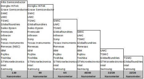
2011 Foundries by process technology

19 different foundries have 130nm capabilities, a process that was introduced in 2000.  This is a fine process for many applications but certainly not very useful for most low-power (such as mobile) applications.  At a 32mn process the number of foundries has dropped to only 6 with only 4 of those expected to hit 22nm this year.  TSMC is a pure play foundry, they make no products of their own, solely parts for other companies.  Globalfoundries is the foundry spinoff of AMD, and now operates much like TSMC.  Samsung does both, they make many products themselves (The Apple A4 processor being one of the better known products) as well as provide foundry services for other companies.  Intel recently started to experiment with working as a foundry, perhaps to take up any slack they may have in their fabs.  One particularly interesting note is that Japanese fabs have not been able, or willing to keep up with technology.  This may have to do with how fragmented that market was, and may change as more Japanese IC companies consolidate (such as Mitsubishi, Hitachi and NEC forming Renesas).

This trend will continue as technology advances and becomes more expensive to produce.  However, many products simply do not need to be made on the most advanced process. Your toaster oven is just fine with running ICs made on a 130nm process, and thats unlikely to change.  As long as there are 3-4 foundries on the leading edge, competition will keep driving advances in technology, and reductions in costs.

January 24th, 2011 ~ by admin

IBM’s Server Processors: The RS64 and the POWER

IBM POWER1 Data Cache circa 1990 - 30MHz

IBM in the late 1990s was making a wide variety of processors, from the Cyrix Design 6x86MX, to fab work for AMD on the K6, to the PowerPC line used in Apple computers.  Most of these processors were low margin designs for the consumer market.  What IBM is best known for, and best at, is server and workstation processors.  The kind of processors you will find by the thousands in Top 500 Supercomputers.

There were three distinct architectures IBM used in this market.  The POWER (Performance Optimization With Enhanced RISC) processor originated in 1990 as a new deign for IBM.  IBM also was working on with Apple and Motorola in a consortium known as AIM to design a PC based processor architecture, loosely based, or inspired by, POWER.  This became known as the PowerPC.  IBM also was looking for a solution to replacing their old AS/400 CISC based computers.  A processor architecture to smooth the transition from CISC, to full on RISC was needed. A subset of the PowerPC design was developed with added instructions from the POWER2 and AS/400 called PowerPC-AS.  The first CPU to use this architecture was the A10, released in 1995 at 77MHz

IBM RS64 IV 600MHz Dual Core - 2001

The RS64 line implemented the PowerPC-AS architecture and was initially released in 1997.  RS64 designs were focused mainly on transaction processing and other integer intensive applications.  Their floating point performance was not as good as the POWER architecture.  Debuting at 125MHz with 128kb of L1 cache, and 4MB of off chip L2 cache.  By 2000 IBM had continually improved upon the RS64 architecture, as well as fab processes.  The RS64-IV, the final RS64 processor, was released at 600MHz and topped out at 750MHz.  At the time the POWER line (now at the POWER3) has stagnated, the RS was able to clock twice as fast, and at less power (15W per core)

POWER3-II 375MHz - 2000

In 1998 IBM released the POWER3, the third generation in the POWER line, and the contemporary to the RS64-IV.  The POWER3 essentially merged the full 64-bit PowerPC instruction set into the POWER line.  Initially it ran at 200MHz with 96kb of L1 cache, 16MB of off chip L2 cache. It was manufactured on a hybrid 0.35/0.25u process. In 2000 IBM released the POWER3-II, a process shrink to 0.22u, with other enhancements, that brought the POWER line up to 450MHz.  Still the POWER3 languished in pure speed (at least in integer) against the RS64-IV.

Having two independent processor lines is extremely expensive to maintain.  Support costs, software costs, R&D, etc all were double what they would be with a single unified architecture.  In 2001 IBM released the POWER4 and discontinued the RS64 line.  The POWER4 merged the PowerPC (and POWER) instruction sets with the PowerPC-AS instruction set of the RS64.

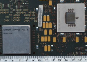
IBM POWER4+ 1.2GHz - 2004

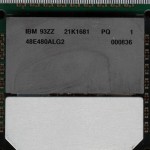
Now IBM had a single processor for both the RS/6000 line and the AS/400 line of computers.  The POWER4 was also an incredible boost in speed and now featured 2-cores on one die (the first non-embedded processor to do so).  Even the initial version did 1.1GHz.  L2 cache size was decreased to 1.4MB but moved on die.  L1 cache remained at 96kb.  To compensate for the reduced L2 cache size IBM added a 32mb off chip L3 cache.   The POWER4+ would eventually hit 1.9GHz.  In the picture on the left the 32MB of L3 cache is the large white chip in the upper right, while the dual core CPU is in the lower left.

POWER5 1.65GHz - 2004

In 2003 IBM further enhanced the POWER line and released the POWER5 processor.  Again a dual core processor running at 1.5-2.3GHz.  The POWER5 increased the on chip L2 cache to 1.9MB and moved the L3 cache on chip (though a separate die, like the Pentium Pro).  The L3 cache was also increased to 36mb.  As with the POWER4 the POWER5 was also offered in larger MCMs that integrated 4 processor dies, and 4 36mb L3 cache dies onto a single, large, MCM.  IBM has an excellent, in depth article on the differences of the POWER4 and POWER5 here.  IBM continues to develop the POWER line and currently is shipping system based on the 4GHz+ POWER7 processor.  The POWER8 successor is under development.

Posted in:
CPU of the Day

January 16th, 2011 ~ by admin

CPU of the Week: Intergraph Clipper C4 MCM


Fairchild developed the Clipper architecture in 1986, and sold it to Intergraph in 1987.  The design never enjoyed wide success and was only used in systems made by Integraph, as well as some by ‘High Level Hardware.’  The deign itself was RISC like and competed mainly with the Sun SPARC processors.

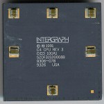
The final version was the C400 which was released in 1993 (preceded by the C100 and C300). Presumably there was a C200 but I have not seen any documentation on it.  The C400 ran at 50MHz (like the C300) and actually consisted of 3 separate chips. The CPU, the FPU and the CAMMU (Cache/Memory Management Unit).  Intergraph developed their own version of UNIX called CLIX to run on the clipper, and demonstrated a version of Windows NT that ran on the C400 as well. Ultimately the lack of software support, and the slow adoption killed the Clipper.  While Intergraph was designing the C5, Intel assured them a good supply of processors, and this convinced Intergraph to cancel the C5.

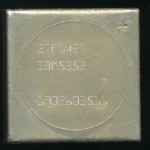
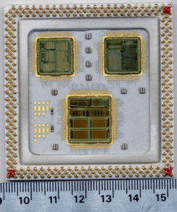
Intergraph C4 MCM

It was also available as a MCM (multi-chip-module) incorporating all three dies in a single ceramic package.  This is one of the nicest looking MCMs I have seen, unfortunately the bottom plate was missing when I got it, but the dies are at least visible.  I unfortunately am not sure which die is which so if you know, let me know.

Posted in:
CPU of the Day

January 6th, 2011 ~ by admin

The day has come, ARM + Microsoft Windows

Over a year ago we wrote about the need for native support of ARM cored processors by Windows (and not just Windows mobile).  Yesterday at the CES Microsoft officially announced it will be supporting ARM processors as well as ARM SoC’s in Windows 8, and demo’d several such systems.  This is very important to the landscape of processors.  Obviously software support will be initially lacking but this brings much needed competition to the PC market.

Intel and AMD have been competing with each other, and each other alone (with a few exceptions) for almost 10 years now. Bringing full fledged Windows to a new architecture is not unprecedented.  Windows NT 4 ran on x86, MIPS, PowerPC as well as the Digital Alpha.

Nvidia, already very talented in the GPU market, has been working on ARM processors for a couple years now with its Tegra line, so its not surprising that they have also announced development of a ARM based processor/GPU targeted for the desktop known as Project Denver.

VIA is also adding some more competition with the release of their first dual core processor, the Nano X2, based on the Isaiah architecture.  While not known for brute force, the Nano is known for its low heat and power sipping capabilities.

2011 is off to a great start and we look forward to seeing many new processors released, as well as old processors added to the museum

Posted in:
Processor News

December 12th, 2010 ~ by admin

CPU of the Day: Ferranti FBH 5092 – The F100L MCM

In the 1970’s the British electronics company Ferranti was commissioned by the Ministry of Defense to develop a processor for military applications.  The desire was for something along the lines of the American MIL-STD-1750A processor.

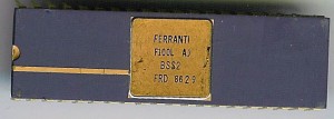
Ferranti F100L - 1986

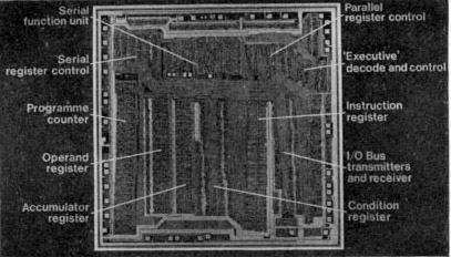
In 1977 Ferranti released the F100-L 16-bit processor. It was made using Bipolar technology (rather then MOS) so it could easily hit speeds of 8MHz (albeit getting rather warm in the process).  The F100-L was one of the first 16-bit processors made (along with the National Semiconductor PACE). The processor contained over 1500 gates and was made using  collector diffusion isolation (an enhanced Bipolar design) and was produced with 3.5 micron features. The die itself occupied 60mm^2.

Ferranti F100-L Die

The F100-L was designed to handle real time data quickly and efficiently (time critical processing of signals and information is always one of the key requirements of a military specific design).  It however was not as adaptable or flexible for use in standard computing environments.  Ferranti tried to sell it commercially with only limited success.  It ended up in some of the same uses as the Signetics/SMS 8X300 series of processors.

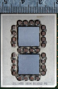
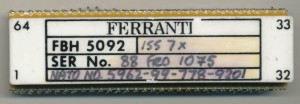
Ferranti FBH5092 - F100-L Hybrid Module

Ferranti also made the F100-L in a Hybrid, or MCM (Multi-Chip-Module) that contained a F100-L processor, a F101-L Multiply/Divide unit (a simple FPU), clock generators, and a pair of F112-L Data Interfaces to act as buffers.  All of ths was packaged in a single 64 pin DIP.

Tags:

Posted in:
CPU of the Day

November 29th, 2010 ~ by admin

Broadcom’s MIPS Chips

A lot of talk goes on about ARM cores and their increasing use and speed.  While the market penetration, shear speed, and low power of ARM cored devices is certainly amazing its important to not forget that their are other cores in wide use as well, if not as glamorous.  The MIPS architecture was developed at around the same time as ARM (1985) and actually enjoyed success in the market much sooner then ARM did. MIPS continues to be widely used in embedded applications (expecially the MIPS 4000 architecture).

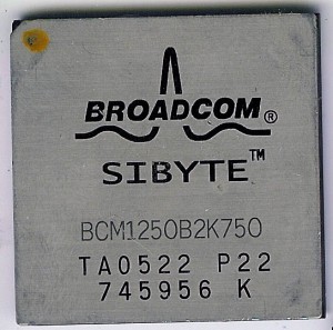
Broadcom Sibyte BCM1250B2K750 - 750MHz dual core MIPS

Broadcom is one of the largest users and producers of MIPS cores devices.  Broadcom recently announced the BRCM5000 MIPSs CPU core. It can issue 2 instructions per cycle and at 40nm runs at at least 1.3GHz (worst case speed).  It should handily clock to 2GHz+ given good process and part selection (the core uses AVS to scale voltage internally to find the perfect voltage/speed combination on a part level basis).  Broadcom chose to not use a multi-core design as a multi-core doubles die area, almost doubles power, but in typical applications does not double performance.  Using a dual-threaded design, on a dual-issue core, does provide almost a doubling of performance, at a minimum of die area.  Die area being a huge concern when the core must be integrated into various products used for mobile devices.  The BRCM5000’s predecessor (the BRCM3000) occupies a mere 1 square mm of die space at 40nm.

Broadcom is not new to the MIPS seen, they have been using them since the 1990’s when Broadcom was founded. Since then they have continually enhanced their products, via internal development, as well as many acquisitions.  Some of the more notable MIPS acquisitions were Sibyte in 2000 who made high-end MIPS network processors and the Xilleon product line from ATI/AMD in 2008 which made Digital TV Processor chips based on the MIPS core.

Just recently Broadcom closed their purchase of Beceem, a company that makes 4G chipsets based on the MIPS core.  MIPS continues to be used not just by Broadcom. Microchip’s PIC32 line is in fact a MIPS R4K processor. Cavium Networks, RMI, Toshiba, NEC, and Sony all continue to use MIPS in a variety of products.   MIPS continues to try to penetrate the smartphone industry, and if at all possible should.  The competition would help keep new innovations coming.

Tags:
,

Posted in:
Uncategorized