April 16th, 2013 ~ by admin
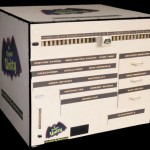 Master Modder Bacteria recently completed ‘Unity’ a single cabinet integrating 15 classic consoles, and capable of playing games from 18 different systems (sme consoles can run more then one type of game. It an impressive feat especially considering he managed to make it work off a single controller, and a single video/audio output. A custom 15-position switch tops off the console.
The consoles range from a Intellivision and its oddball CP1610 General Instruments (based on the PDP-11) processor, to the wildly successful 299MHz Sony PS2. Below you can see the variety of systems, and the processors (this IS the CPU Shack after all) that run them.
As you can see a few processors are common. Five of the consoles run Zilog Z-80 processors, and 4 run on some variation of the MOS 6502 made famous by the Apple 1 computer. Later consoles shifted towards the RISC based designs of MIPS, PowerPC and the SuperH series by Hitachi (now Renesas). Today’s console continue to use RISC processors albeit at speeds of over 3GHz.
April 7th, 2013 ~ by admin
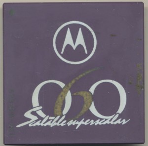
Motorola 68060 Marketing Sample
The Motorola 68060 was the last of the 68k line that was begun in the late 1970’s. The 68k began as the first commercial success of a 32 bit processor. It wen through many upgrades, essentially proving to be worth competition (and likely a better architecture) to Intel’s x86 line. The ‘060 was the first 68k to bring a superscalar architecture. It could issue multiple instructions per clock, in some ways it was better then the Intel Pentium. The 68060 was released in 1994 but never achieved wide success. By the time of its introduction Motorola had thrown most of its weight behind the PowerPC of the AIM Alliance. Eventually the 68060, which was released on a 0.6micron process at 50MHz, would be moved to 0.42 micron and hit 75MHz.
It, unfortunately, suffered the same fate as the 88000 RISC processor, a slow but inevitable fading away. The 68k line (mostly the 68000 core, or its derivative, the CPU32) lives on in many of Freescale’s products.
The chip shown is what is known as a Marketing Sample. These typically were only an empty package, given to sale people and distributors as gifts or sales aids. They typically feature a flashy logo, more color, and often, like this one, a sales pitch. ‘Scalable Superscalar’. It seems that the 68060 proved less salable then it was scalable.
April 2nd, 2013 ~ by admin
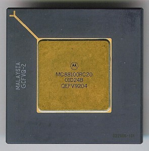
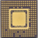
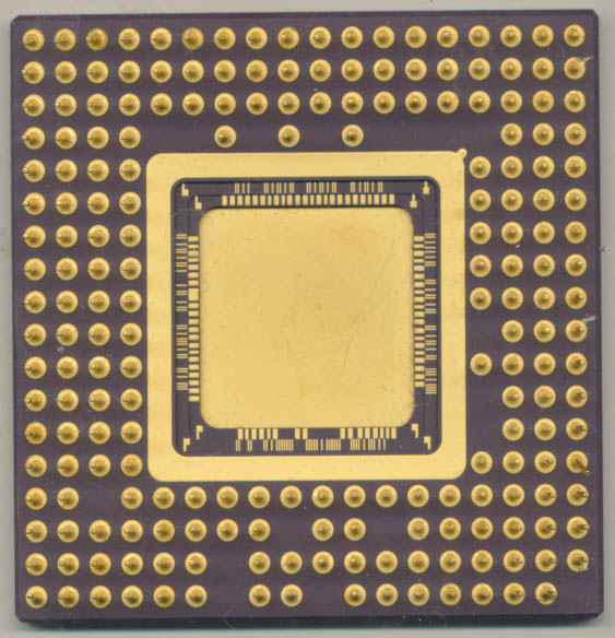
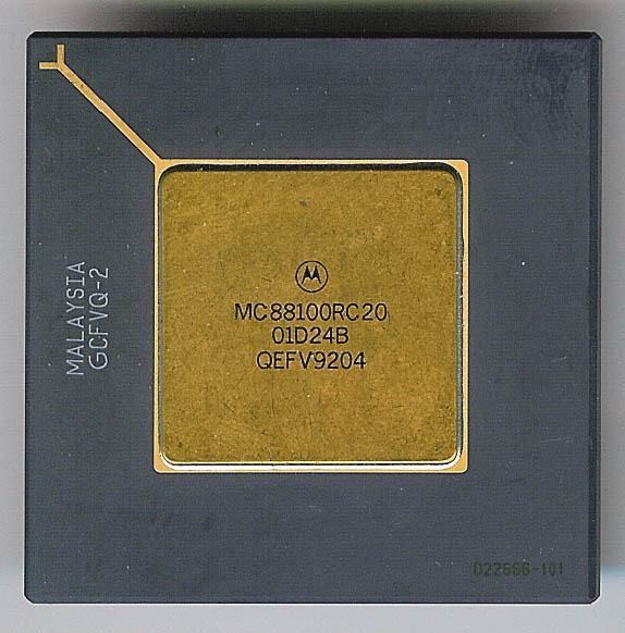
MC88100 20MHz – 1992
In the late 1980’s Motorola was developing a full 32-bit RISC processor from the ground up. Initially called the 78000, it was renamed the 88000. The first implementation of the 88000 Instruction Set Architecture was the 88100. It included a FPU and integer unit but required a separate chip (the 88200 CMMU) for caching and memory management. Typically 2 of the 88200s were required (one for instruction cache, one for data, 16kb of cache each). A 64lb cache was also available called the 88204. Made on a 1.5u process the 88100 contained 165,000 transistors while the CMMU chips contained 750,000. Each chip dissipated 1.5Watts at 25MHz. Prices in 1989 were $494 for the CPU and $619 each for the CMMUs. A complete system of 3 chips would be nearly $2000. Not exactly competitive pricing.
The initial, and biggest, customers for the 88000 were to be Apple, and Ford Motor Company, an unusual combination to say the least. Apple invested in the 88000 to be the replacement for the 680×0 processors it had been using. Ford was looking to replace the Intel 8061 processors (from which the MCS-96 MCUs were developed) that had run their EEC-IV engine computers since the early 1980’s. Motorola (as well as Toshiba) had been second sourcing these for Ford for sometime. Ford based its choice on the 88100 based ECU on the assumption that Apples adoption of the 88100 would guarantee good software and compiler support. If Apple stuck with it that is..
Read More »
March 27th, 2013 ~ by admin
Here at the CPU Shack I handle shipping and receiving for collectors all over the world, this means i have packages coming in daily, dozens of them. Sometimes collectors will go in together to get a large lot of processors etc. Today one such lot arrived, over 2200 wafers from Kokomo Semiconductor. That’s nearly 300lbs.

Noel, the CPU Shack’s head of security, does not seem impressed.
March 23rd, 2013 ~ by admin
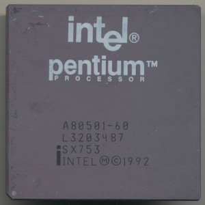
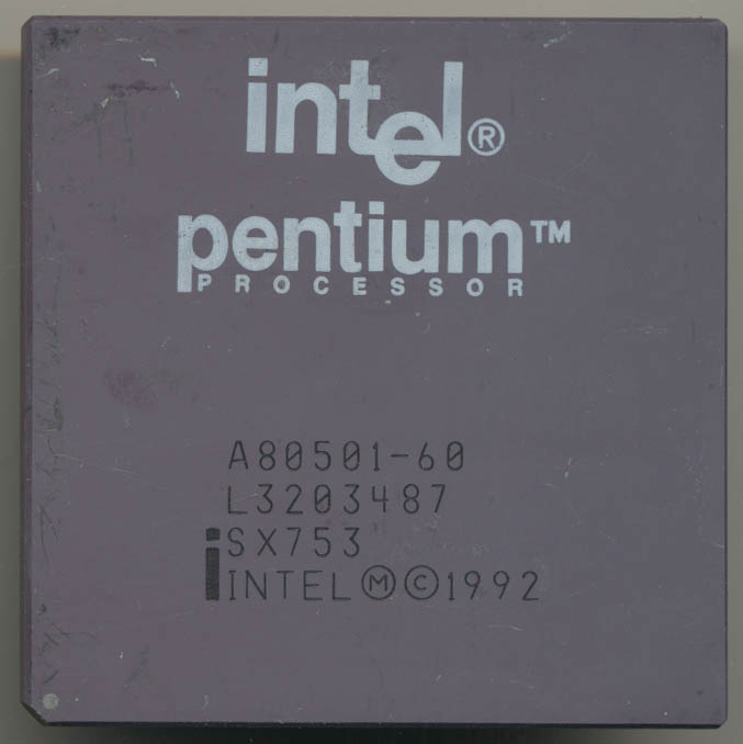
Intel Pentium 60 – Produced May 1993
On March 22nd, 1993 the Intel Pentium Processor was released to the public (so yah yesterday but hey whose counting). This was Intel’s first processor with an actual name. Turns out you cannot trademark a number, so the ‘486’ name was being used by everyone (AMD, Cyrix, TI, UMC, IBM etc). Initially known by its core name, P5, the Pentium was also the first superscaler Intel x86 processor It had dual Integer pipelines, and a single Floating point unit allowing it to issue and complete multiple instructions per clock.
The first Pentiums ran at 60 and 66MHz and were made on a CMOS 0.8micron process with 3.2 million transistors. After only a few months it was discovered that they ran particularly warm and the package was updated with a Copper-Tungsten heatspreader (gold plated).
A modern desktop processor such as the Core i7 Quad Core Ivy Bridge contain 1.4 Billion transistors on a 22nm process. The P5 still lives on in the embedded market, and in the Intel Larrabee project which is itself, an updated P54C core (supporting a few more modern features such as x86-64).
March 22nd, 2013 ~ by admin
IBM System/370 – 1970
IBM introduced the 12.5MHz cabinet sized System/370 in June 1970 as an evolution of the System/360 from 1964. These systems formed the entire base of IBM’s mainframe business. Today’s System z, itself an evolution of the original System/360 and 370, can still run many of the original programs, unmodified, from 50 years ago. This is a testament to 2 things, the wide adoption of the IBM systems, and the forward thinking of IBM. Even the original System/360 from 1964 was a full 32-bit computer. Single chip processors did not embrace 32 bit architectures until the very early 1980’s (Motorola 68k, National 32k, etc).
In 1980 IBM sought to make a single chip version of the 370, in an effort to make a version that could be used for desktop type computers. This was to become the Micro/370. There were 2 distinct products to come out of this goal that are widely confused and debated. The first became the PC XT/370, an add in card(s) for an IBM PC to give it the capability to run System/370 software. Later another version was developed called the Micro/370 as a single chip solution.
The PC XT/370 began as an experiment, a test bed implementation of the System/370 in a microprocessor environment. The goal was not to rebuild the 370 from the ground up (that would come later) but to merely implement its instruction set into an existing design. The base processor had two main requirements: it had to be 32 bits, and it had to be microcoded. IBM’s engineers in Endicott, NY selected the then very new Motorola MC68000 processor as their basis. It was one of the only 32-bit designs at them time so that no doubt helped in the selection process.
Read More »
March 16th, 2013 ~ by admin
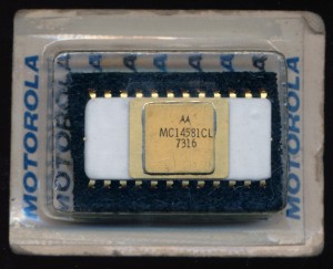
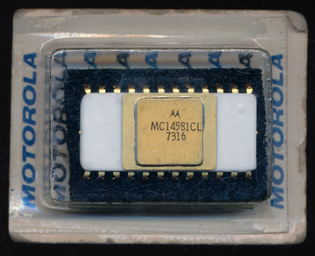
Motorola MC14581CL 4-bit ALU – 1973
At the heart of every processor is an ALU, an Arithmetic Logic Unit. It is what does the addition, subtraction, compares, and other logic function on the bits we call data. Add some memory for registers, stack, and program control and one has a basic processor, or bit slice processor. In the 1970’s and even the 1980’s many systems still implemented their ‘processor’ in discrete logic. The 74181 (TTL), 10181 (ECL) and 14581 (CMOS) were the heart of many of them. The ‘181 could handle any of 16 arithmetic and logic functions on a pair of 4 bit words.
The Motorola MC14581CL was the first of the CMOS ALU’s. This example was made in early 1973. CMOS itself was only patented a few years prior (1967) and didn’t see extensive use in processors until the mid 1970’s (RCA 1802) and most other processors in the 1980’s. Remarkably, after 40 years, its still in its original package.
March 13th, 2013 ~ by admin
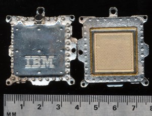
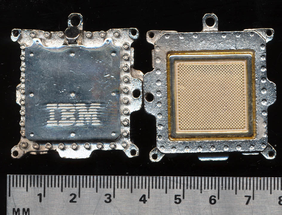
IBM 3081 TCM Pendant
A few times I get things that are not processors but are memorabilia and are pretty special nonetheless. Today these nice IBM pendants came in. They are very small, measuring barely 37mm square but they weigh an impressive 60 grams. They are a near perfect miniature version of a not so miniature IBM TCM (Thermal conduction module). The 3081 TCM contained the cooling, and a very large MCM used in the 308x mainframe series (made from 1980-1987). Each MCM contained up to 133 dies on a very large ceramic substrate with up to 16,000 contacts for the dies. They were capable of speeds of up to 38MHz. Each TCM was liquid cooled and dissipated around 300 watts of heat. A typical 308x system had 2 dozen of these.
A similar IBM MCM can be seen here: (a 9121 processor)
March 10th, 2013 ~ by admin
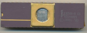
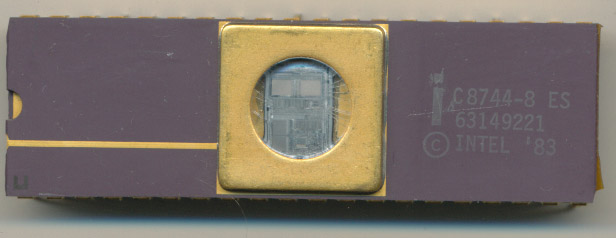
Intel C8744-8 Engineering Sample – Early 1983
In 1980 Intel released the MCS-51 family of microcontrollers, a design that would go on to become one of the pillars of the 8-bit MCU market. Initially the family consisted of the 8051, which included 4KBytes of on-chip ROM (or UV-EPROM in the case of the 8751) and 128 bytes of RAM as well as the 8031 which did not include the ROM, all program memory was off chip.
The 8051 was a wild success with Intel struggling to meet demand. Intel did not have the fab capacity to produce both the 8051, and the very in demand 8088 (thanks to IBM). In 1984 Intel opened a new fab in Albuquerque, New Mexico to build other chips, freeing up production space in the California fab for more 8051s. Even so, an $8 8051 was routinely scalped for over $200 on the grey market and waiting periods of up to a year were common in order to receive orders, with many companies on allocation. Intel licensed the design to both AMD (who built a fab in Austin to make it) as well as Signetics in an effort to keep up with demand. The hardest to get part in the industry, was the 8051 from 1983-1984.

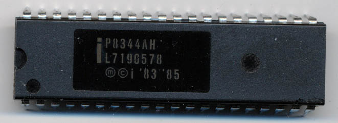
P8344 – A ROMLess 8044, so essentially an 8031 + SDLC controller.
So in the midst of this insatiable demand for an MCU that they did not have the capacity to produce, Intel releases the RUPI-44 (Remote Universal Peripheral Interface). The RUPI-44, also known as the 8044, is an 8051 with an additional 64 bytes of RAM and a full serial communication co-processor on die. Specifically it was an 8051 that handled the SDLC (Synchronous Data Link Control) protocol in hardware. Intel had an SDLC controller, known as the 8273, but it was limited to 64kbps, the 8044 could handle data transfers of up to 2.4Mbps due to the 8051 core’s high speed and close coupling of the serial controller.
SDLC was developed in 1975 by IBM and was generally used as a way for mainframes to communicate with various peripherals and terminals. It supports error correction and multi-point, point to point, and loop connections. In 1979 SDLC was standardized as HDLC (High-Level Data Link Control) which the RUPI-44 also supports. While popular in the 70’s and 80’s its use has faded out, though it achieved some long lived use in Europe running the Intel derived BITBUS protocol well into the 90’s.
Read More »
March 7th, 2013 ~ by admin

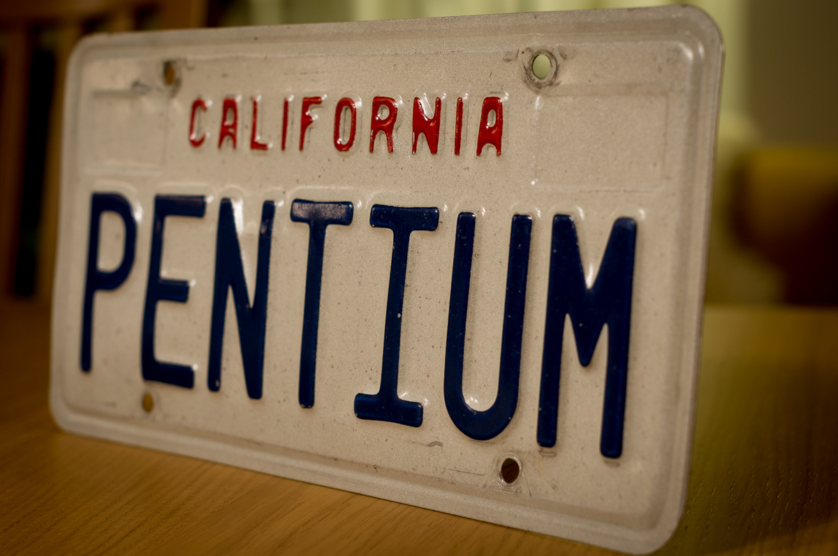
Original PENTIUM California License (number) plate
This California license plate came through the museum on its way to a collector in Sweden. I get many items in that are unusual and rare but this was the first processor relates plate I have seen. The best part? It came with some history.
It was ordered as a vanity plate by a salesman at Intel around 1995. He was later hired by AMD as a sales person but his car still said “Pentium” which obviously was a bit of a problem. As a token of commitment to his new company he gave it to his manager at AMD, despite the fact that he was offered $3000 for it from an employee at Intel. It likely sat on a desk for some time until it was sold on eBay (for the low price of $100) where it was spotted by a collector in Sweden who asked me to purchase it for him.
It now resides with the collection of CPU Collection.SE

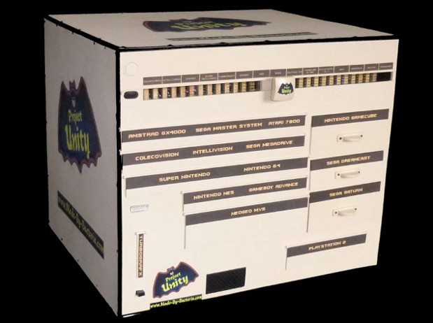 Master Modder Bacteria recently completed ‘Unity’ a single cabinet integrating 15 classic consoles, and capable of playing games from 18 different systems (sme consoles can run more then one type of game. It an impressive feat especially considering he managed to make it work off a single controller, and a single video/audio output. A custom 15-position switch tops off the console.
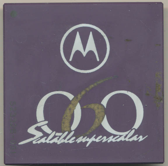

