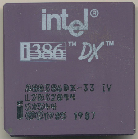
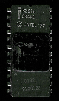
CPU of the Day: Intel RUPI-44 The 8051’s lesser known cousin
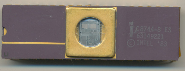
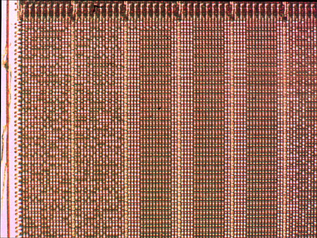
Intel C8744-8 Engineering Sample – Early 1983
In 1980 Intel released the MCS-51 family of microcontrollers, a design that would go on to become one of the pillars of the 8-bit MCU market. Initially the family consisted of the 8051, which included 4KBytes of on-chip ROM (or UV-EPROM in the case of the 8751) and 128 bytes of RAM as well as the 8031 which did not include the ROM, all program memory was off chip.
The 8051 was a wild success with Intel struggling to meet demand. Intel did not have the fab capacity to produce both the 8051, and the very in demand 8088 (thanks to IBM). In 1984 Intel opened a new fab in Albuquerque, New Mexico to build other chips, freeing up production space in the California fab for more 8051s. Even so, an $8 8051 was routinely scalped for over $200 on the grey market and waiting periods of up to a year were common in order to receive orders, with many companies on allocation. Intel licensed the design to both AMD (who built a fab in Austin to make it) as well as Signetics in an effort to keep up with demand. The hardest to get part in the industry, was the 8051 from 1983-1984.
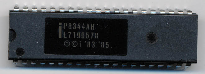
P8344 – A ROMLess 8044, so essentially an 8031 + SDLC controller.
So in the midst of this insatiable demand for an MCU that they did not have the capacity to produce, Intel releases the RUPI-44 (Remote Universal Peripheral Interface). The RUPI-44, also known as the 8044, is an 8051 with an additional 64 bytes of RAM and a full serial communication co-processor on die. Specifically it was an 8051 that handled the SDLC (Synchronous Data Link Control) protocol in hardware. Intel had an SDLC controller, known as the 8273, but it was limited to 64kbps, the 8044 could handle data transfers of up to 2.4Mbps due to the 8051 core’s high speed and close coupling of the serial controller.
SDLC was developed in 1975 by IBM and was generally used as a way for mainframes to communicate with various peripherals and terminals. It supports error correction and multi-point, point to point, and loop connections. In 1979 SDLC was standardized as HDLC (High-Level Data Link Control) which the RUPI-44 also supports. While popular in the 70’s and 80’s its use has faded out, though it achieved some long lived use in Europe running the Intel derived BITBUS protocol well into the 90’s.
 In 1993 Moore designed the F21, again a 21 bit CPU based on the MuP21, designed to run Forth, and including 27 instructions. It was fab’d by Mosis on a 0.8u process. The F21 microprocessor contains a Stack Machine CPU (with a pair of stacks like the NC4000), a video i/o coprocessor, an analog i/o coprocessor, a serial network i/o coprocessor, an parallel port, a real time clock, some on chip ROM and an external memory interface. Performance was 500 MIPS (this was an asynchronous design, so ‘clock speed’ is a bit of a misnomer) and transistor count had risen to about 15,000. The F21 was made up through 1998, however the design continued to evolve. A version of the F21 was developed called the i21, originally for Chuck Moore’s iTV Corporation, which was one of the very first set top Internet appliance companies. It integrated additional featured such as infrared remote interface, modem DMA interface and a keyboard DMA interface. The F21 scaled well, and was tiny, remember, only 15,000 transistors, which at 0.18u takes up a VERY small die, and allowed performance to hit 2400MIPS @ 1.8V. One could put a very large amount of these on a single die…..