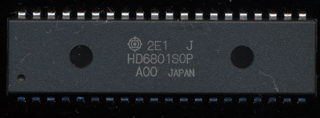
CPU of the Day: Tandem CLX 800 – It Takes 2 To Tango
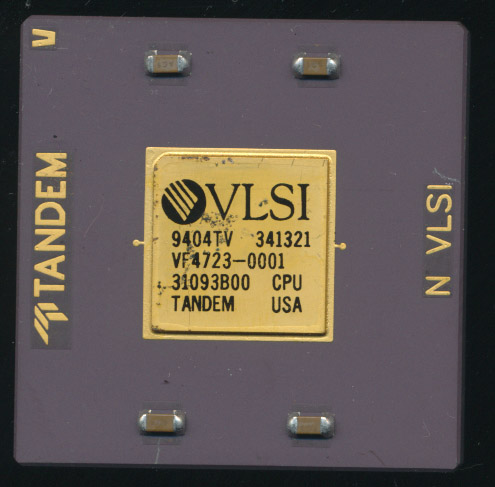
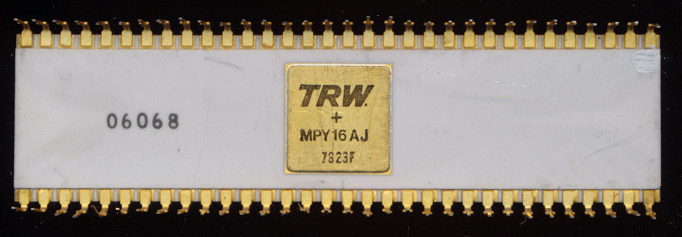
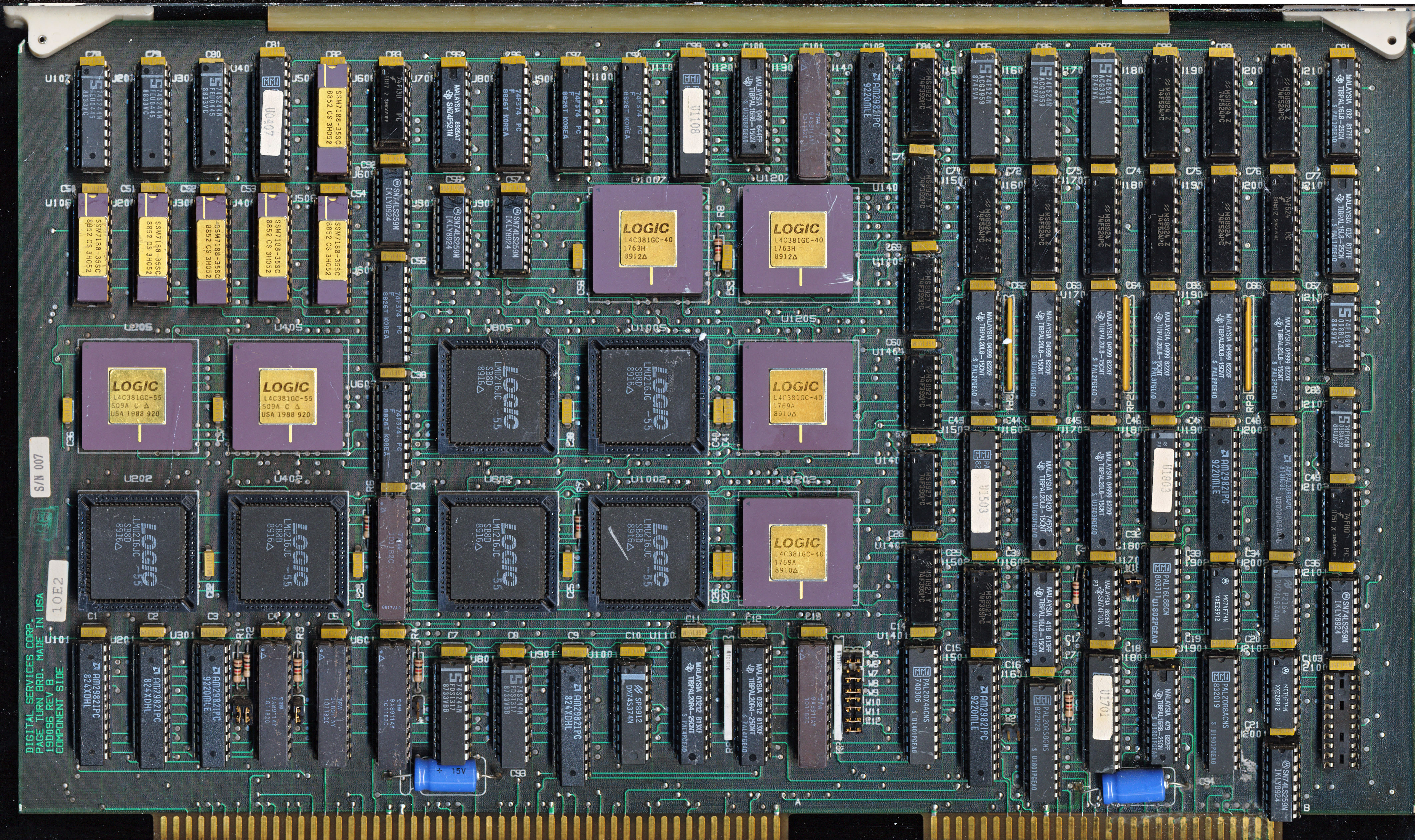
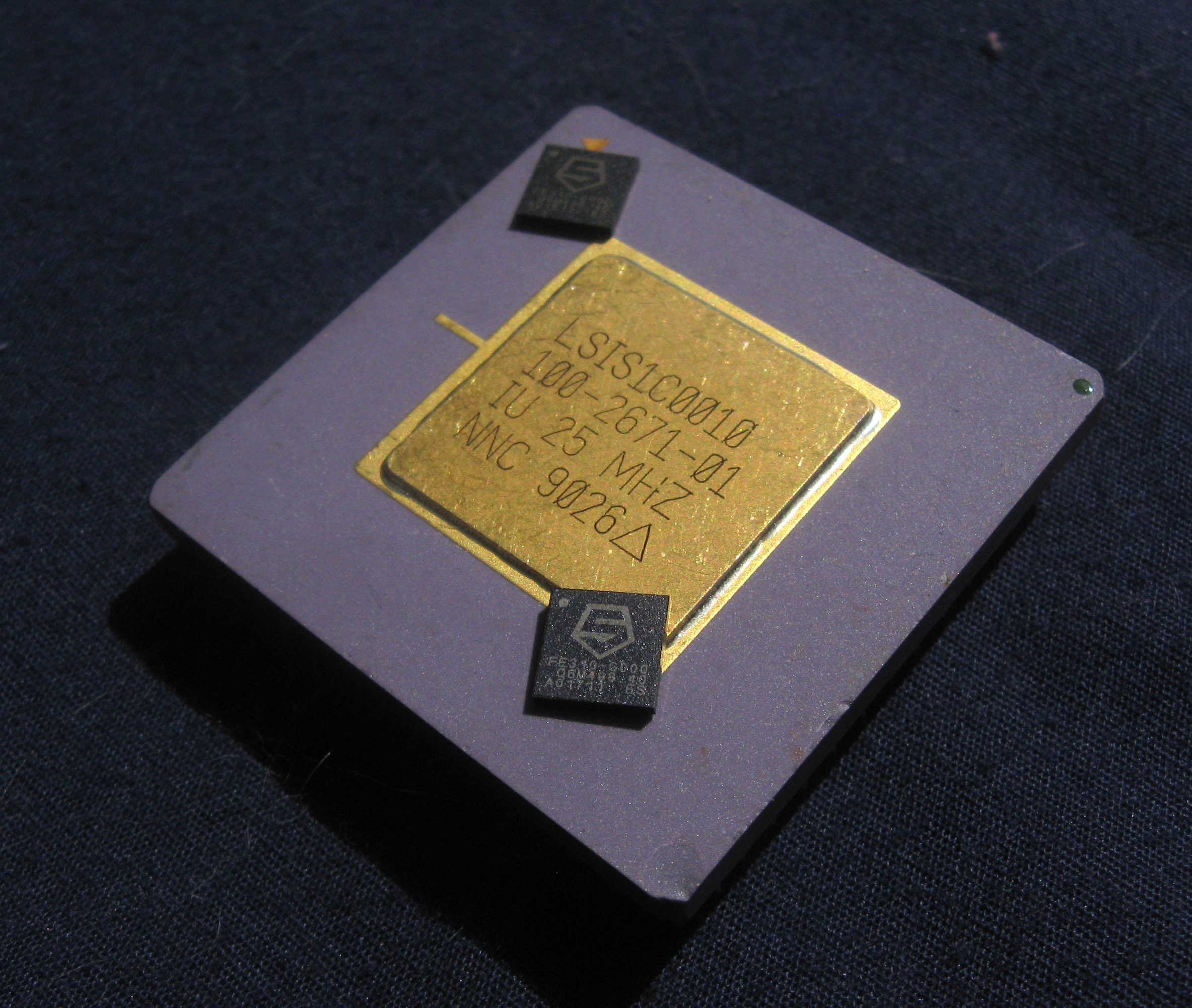
TANDEM CLX 800 Processor – VLSI CMOS 1u process – 16MHz.
Tandem Computers was established way back in 1974, and was one of the first (if not the first) dedicated fault-tolerant computing companies. They designed completely custom computers designed for use in high reliability transaction processing environments. These were used for support of stock exchanges, banks, ATM networks, telephone/communications interchanges, and other areas where a computer failure would result in significant, costly, disruptions to business services. Tandem was started by James Treybig, formally of HP, and a team he lured away from HP’s 3000 computer line.
Tandem computers are designed to do two things well, fail-over quickly when a failed part is detected. This means that if a faulty processor or memory element is found, it can be automatically disabled, and processing continues, uninterrupted, on the rest of the system. The other design element that Tandem perfected was allowing the computer to find and isolate intermittent problems. If a processor or storage element ceases to work, that is relatively easy to figure out, but if a processor is glitchy, causing errors only occasionally, that can be much harder to find and can result in serious problems for the user. This is known as ‘Fast Fail’ and today is a pretty standard concept, find the error, catch it, and prevent erroneous data from ever making it back into the database. Tandem computers were designed from the ground up to be fault tolerant, disks were mirrors, power supplies, busses,
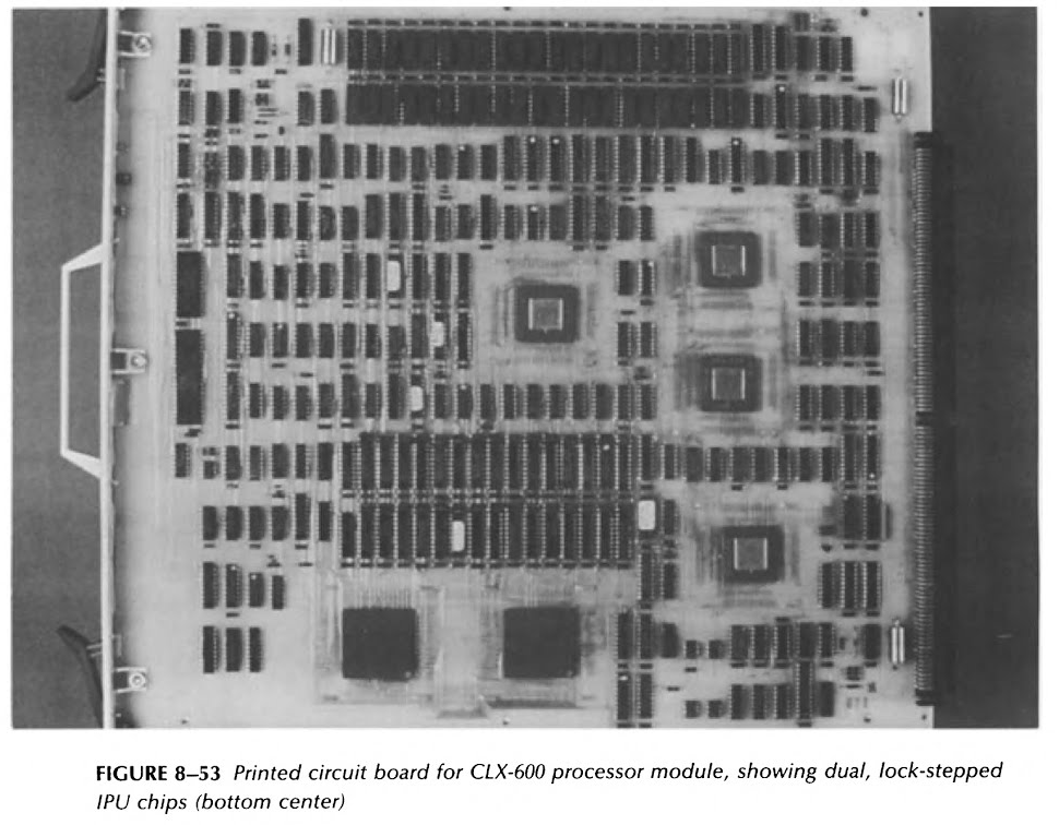
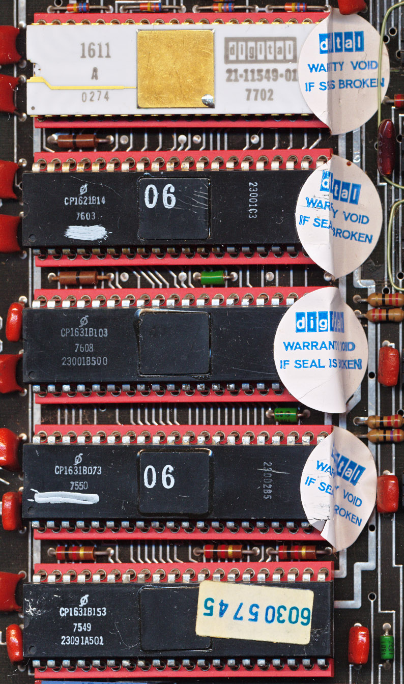
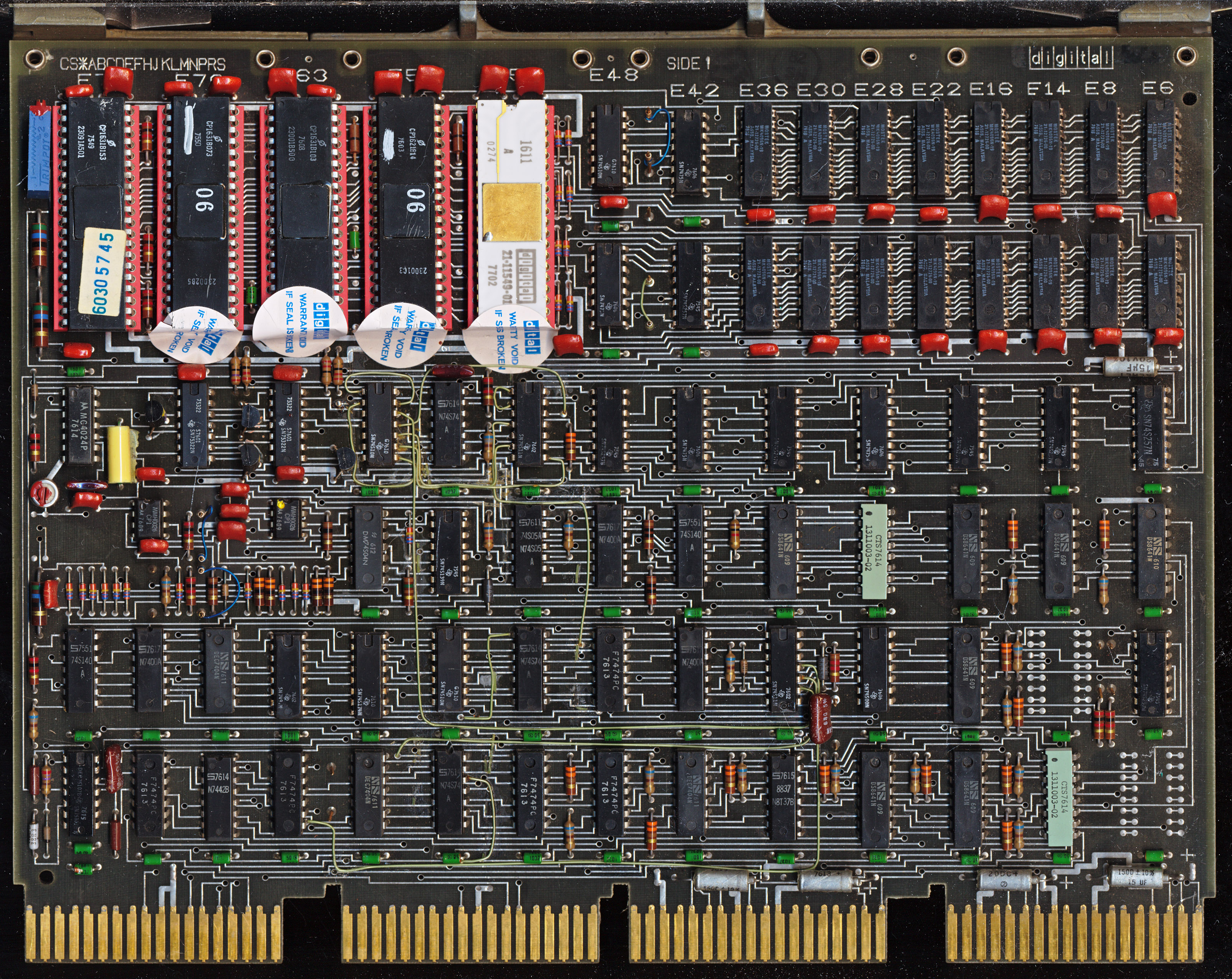
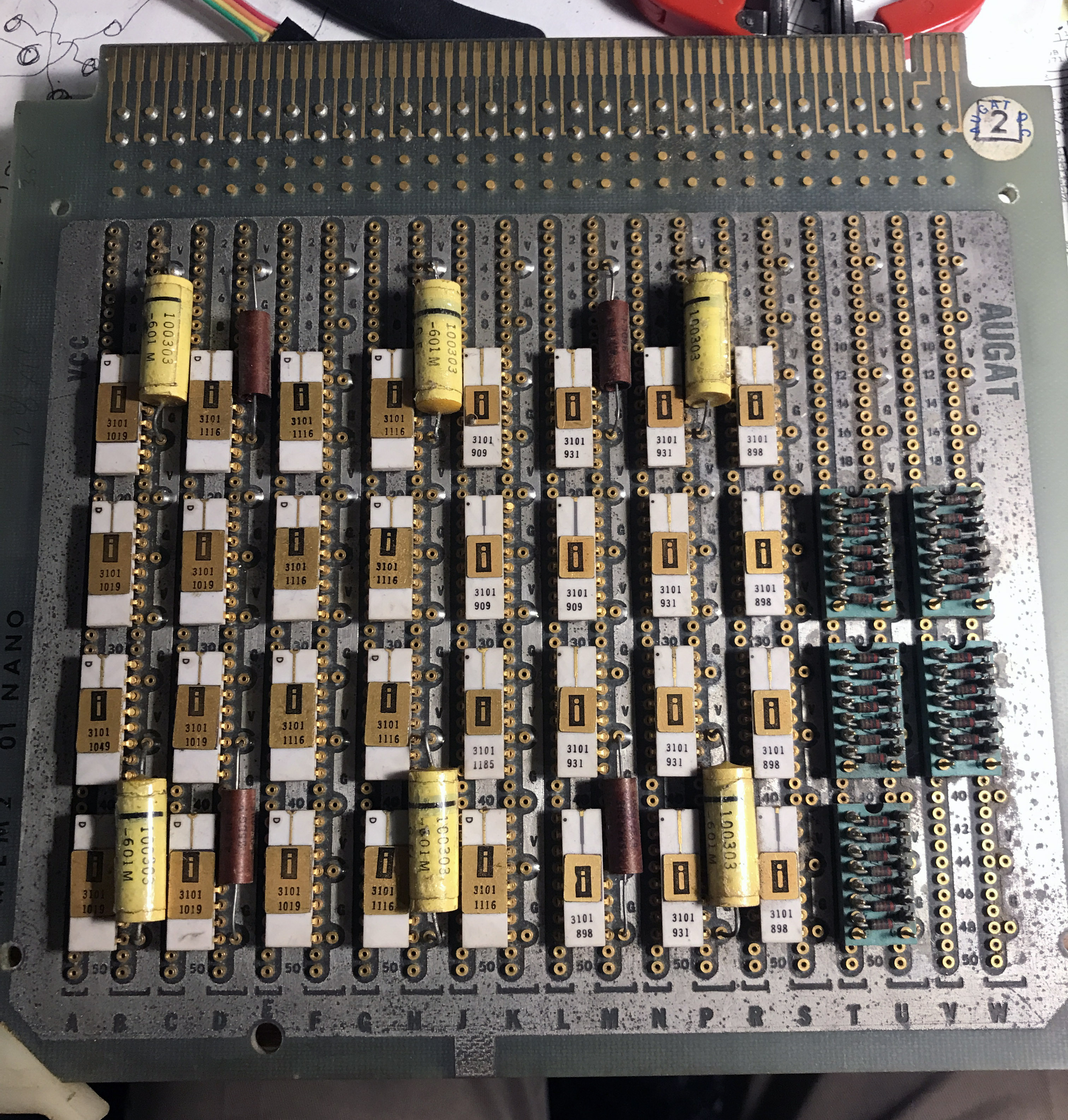
Tandem CLX 600 PCB (click for larger)
processors,all were redundant, but unlike some other systems, components were not kept as ‘hot spares’ sitting idle until something failed. This kept hardware from being ‘wasted.’ Under normal operation if it was in the system, it was contributing to system performance. A failed component then would reduce system performance until it was replaced/fixed, but a customer would not be paying for hardware that served them no purpose unless something broke.
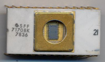
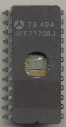
To support these goals Tandem designed their own processors and instruction set architecture know as TNS (Tandem NonStop). The first processors were a 16-bit design call the T/16 (later branded NonStop I) made out of TTL and SRAM chips spanning 2 PCBs. Performance was around 0.7MIPS in 1976. They were a stack based design similar to the HP3000 with added registers as well. T/16 systems supported 2-16 processors. NonStop II, released in 1981, was similar, but supported the occasional 32-bit addressing, increasing accessible memory form 1 to 2MB per CPU and performance to 0.8MIPS.
The 1983 introduction of TXP saw a great performance improvement, up to 2.0 MIPS, but kept the same form factor. The processor was implemented in TTL, with the addition of many PALs and added much better support for 32-bit addressing. In 1986 the NonStop VLX was released, which moved to an ECL based processor. This was a full 32-bit design, running at 12MHz (3MIPS) but still using discrete components and a new bus system as well. This was to be the high end of the NonStop line, it was fast reliable, and rather large. The desire for a more economical system to fit the needs of smaller customers led to a first for Tandem…